1. Introduction
Polyimide (PI) film, known for its exceptional dielectric properties, remarkable thermal and chemical stability, and high breakdown strength, finds wide-ranging applications in critical industries [
1,
2]. These applications include superconducting cable insulation, wind power generator winding insulation, variable-frequency motor winding insulation, and aerospace technologies [
3,
4,
5]. Furthermore, these thin films serve versatile roles as coating films for electronic devices, buffer coatings, intermetallic layers, protective surface coatings in spacecraft, and enameling for electric motor insulation.
The physical properties of PI nanocomposite films, through chemical analysis and thermal analysis, have been extensively explored and documented in various well-researched articles [
6,
7]. However, their electrical conduction mechanisms, charge transport, and dielectric breakdown strength across different electrical fields and temperature conditions have not been addressed in these studies. Therefore, in this research, the main focus is on early breakdown phenomena such as conduction current, which are extensively covered for PI nanocomposite films.
Adding aromatic heterocycles to PI’s main chain makes it much more stable at high temperatures and under pressure, and also makes it less likely to conduct corona. Additionally, due to PI’s excellent electrical insulation properties, it has garnered significant interest as an inter-turn insulation material for variable-frequency traction motors [
8,
9]. Nevertheless, conventional PI and other polymer insulating materials are susceptible to failure after exposure to corona and prolonged damp heat aging, necessitating modifications to meet the ever-increasing demands of various applications [
8,
9,
10,
11,
12,
13].
Under conditions involving high voltage and high-speed pulses, material breakdown primarily results from electrical breakdown, electrochemical corrosion breakdown, and thermal breakdown, each following distinct corona breakdown principles [
3,
4]. Presently, the predominant approach to enhancing the corona resistance of PI matrices involves nano-composite modification [
14,
15,
16,
17,
18]. This entails the incorporation of inorganic materials such as ceramics, clays, and polysilanes, aiming to augment the electrical conductivity, electrochemical stability, and thermal conductivity of polymer materials, thereby fortifying the material’s resistance to corona [
19,
20,
21,
22,
23,
24].
Recent experimental evidence highlights the pivotal role played by space charge accumulation within the bulk of PI films in direct current (DC) breakdown [
25,
26,
27]. Additionally, it is evident that several other conduction processes occur at the interface between electrodes and PI films, contributing to localized electric field reinforcement before eventual breakdown [
28,
29]. Conduction currents arise from diverse polarization and depolarization processes occurring within the material. The complete polarization process encompasses instantaneous currents resulting from displacement polarization, relaxation polarization currents, and conduction currents attributed to specimen conductivity [
28,
30]. The Simons and Tam theory elaborates on depolarization currents, describing them as a superposition of various relaxation processes contingent upon trap levels [
31]. In the steady state, the current density through each electrode and the bulk material must be constant, i.e., it must have the same value at every place. It is therefore not a situation where the current is either injected (i.e., the Schottky process) or carried by bulk transport, but one in which one of the processes acts as the controller of the others. For example, where injection at a given electrode field is higher than bulk transport, space charge builds up to limit the injection to what can be carried by bulk transport; this is the controlling process. The injection of charge at a lower electric field is almost very low, and the current density J, which follows the Ohm law, can be computed from the following expression, as shown in Equation (1):
where n represents the charge density and e expresses the elementary charge. The charge injection becomes high with the increase in E-field, and is then captured by the traps. In addition, J-E curves show the conduction characteristics, including the SCLC model and Schottky emission process.
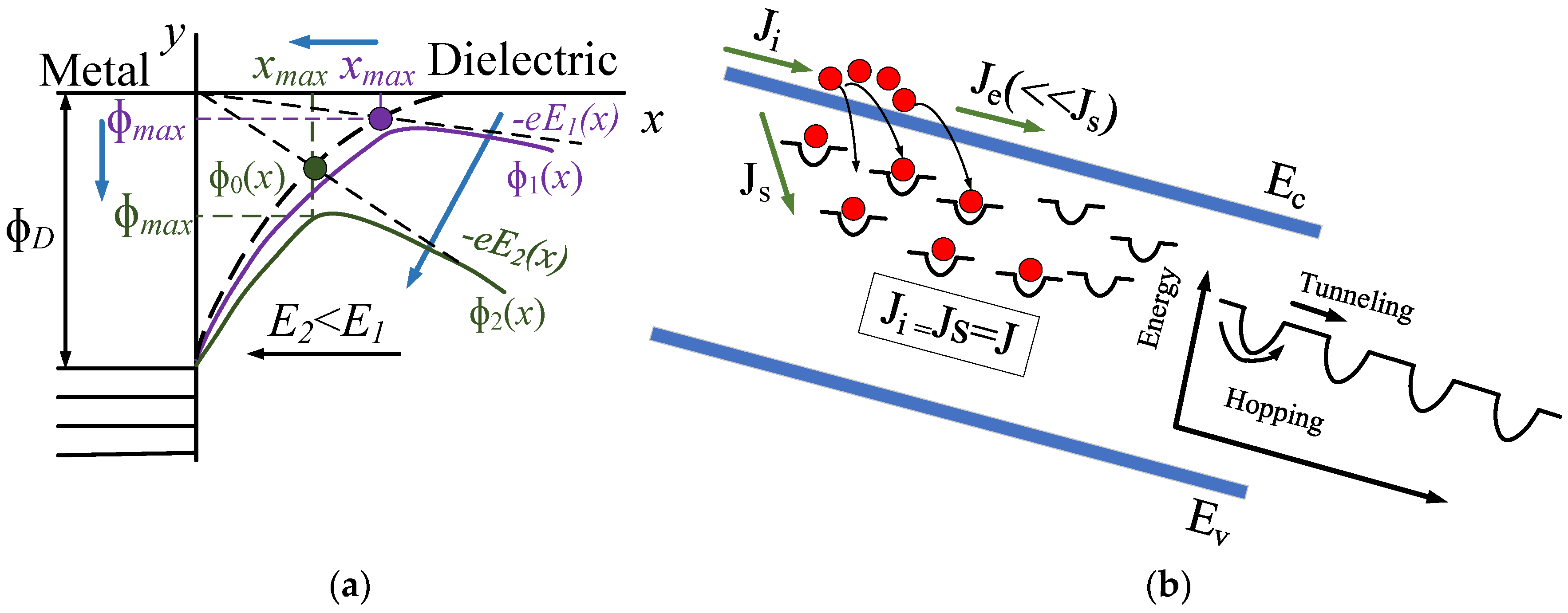
Figure 1a illustrates the Schottky and electrode limited currents. Φ
D represents the metal work function, and Φ
0(x) is the actual barrier, which represents the electrostatic attraction among positive charges and electrons on the metal surface. Φ
max and x
max both started to decrease with the rise in E-field, as shown in
Figure 1a. This leads to a decrease in the height and thickness of the injection barrier for Schottky injection, facilitating greater charge injection from the electrode and contributing to the overall injection current. On the other side,
Figure 1b represents the SCLC model and bulk current. In the SCLC model, a fundamental condition is that the electrode must establish an ohmic contact with the insulator to guarantee adequate space charge in the dielectric [
32]. However, due to the reduced and thinner injection barrier under a high electric field, a substantial amount of charge can be injected via Schottky emission. Consequently, even if the electrode and insulator lack ohmic contact, the significant injected charge and trapping process cause the conduction behavior of the dielectric to align with the SCLC model. According to the illustration in
Figure 1b, the injection current (J
i) in the dielectric surpasses the electron current (J
e), resulting in the accumulation of space charge in the vicinity of the electrode. The presence of space charge results in the SCLC J
s, leading to the relationship J
i = J
e + J
s. Because J
s significantly outweighs Je, the SCLC represents the conduction current in the dielectric. It should be noted that varying distributions of trap levels contribute to different trap-limited SCLC scenarios. In general, as the electric field strength increases from low to high, the Schottky current is encouraged due to the reduced and thinner injection barrier. Simultaneously, a significant accumulation of injected charge within the dielectric aligns its conduction characteristics with the SCLC model. With further electric field augmentation, the number of charges may exceed that of the traps, possibly resulting in the complete filling of the traps by the charges. To summarize, when the electric field is below 100 kV/mm, the conduction process typically involves electrode-limited and bulk-limited conduction. However, as the electric field attains exceptionally high values, the nature of bulk-limited conduction may undergo changes, while the status of electrode-limited conduction remains uncertain.
3. Results and Discussion
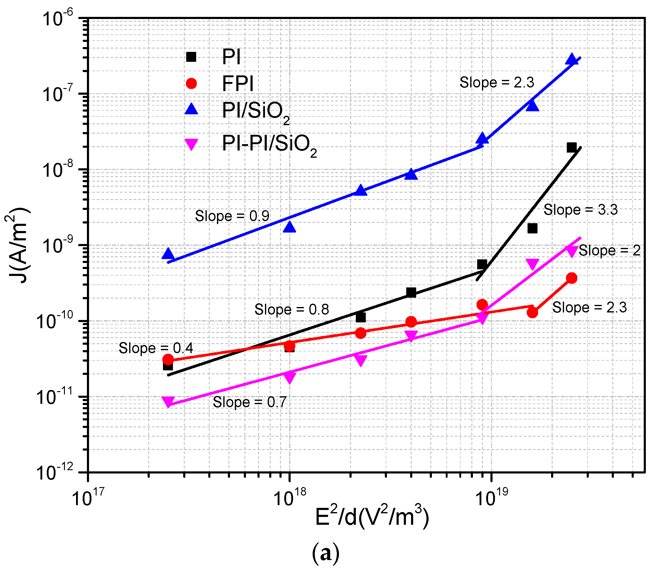
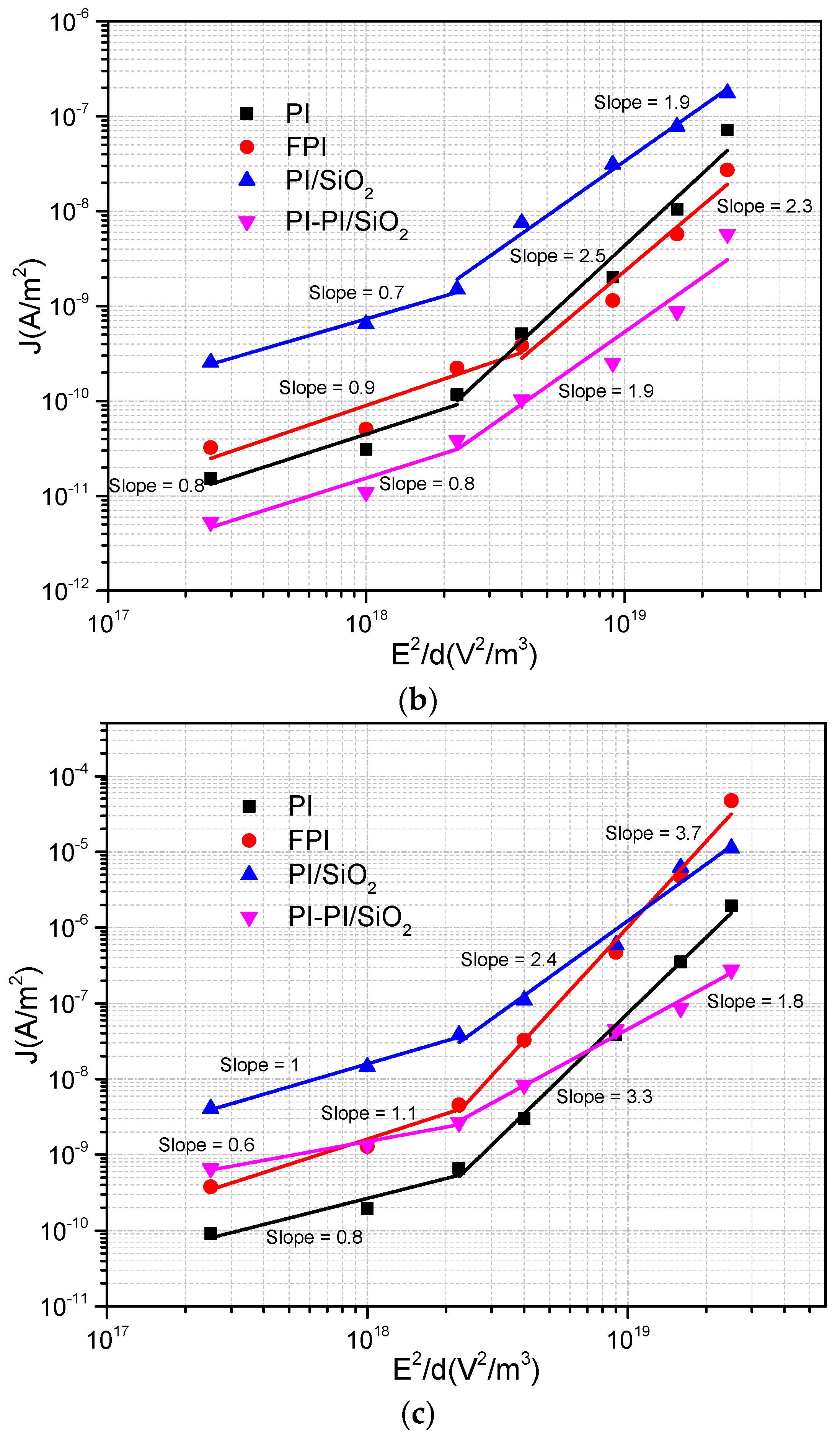
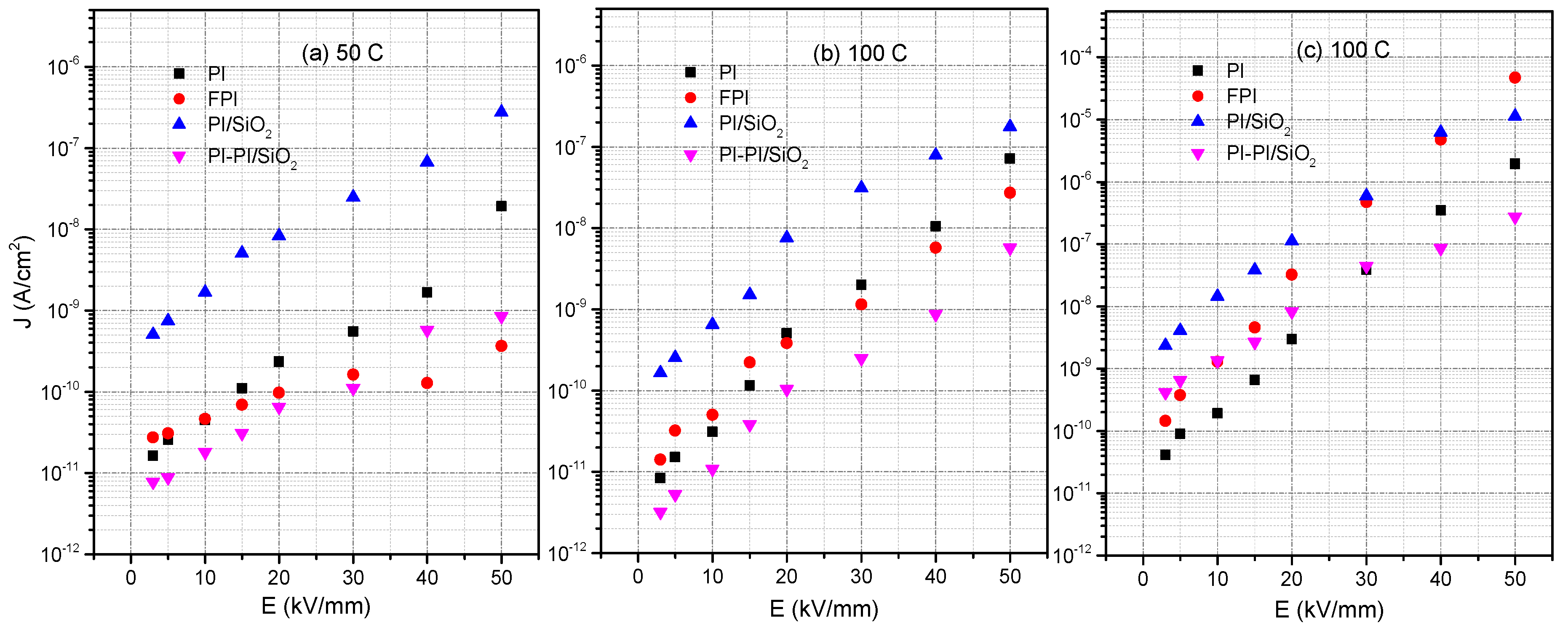
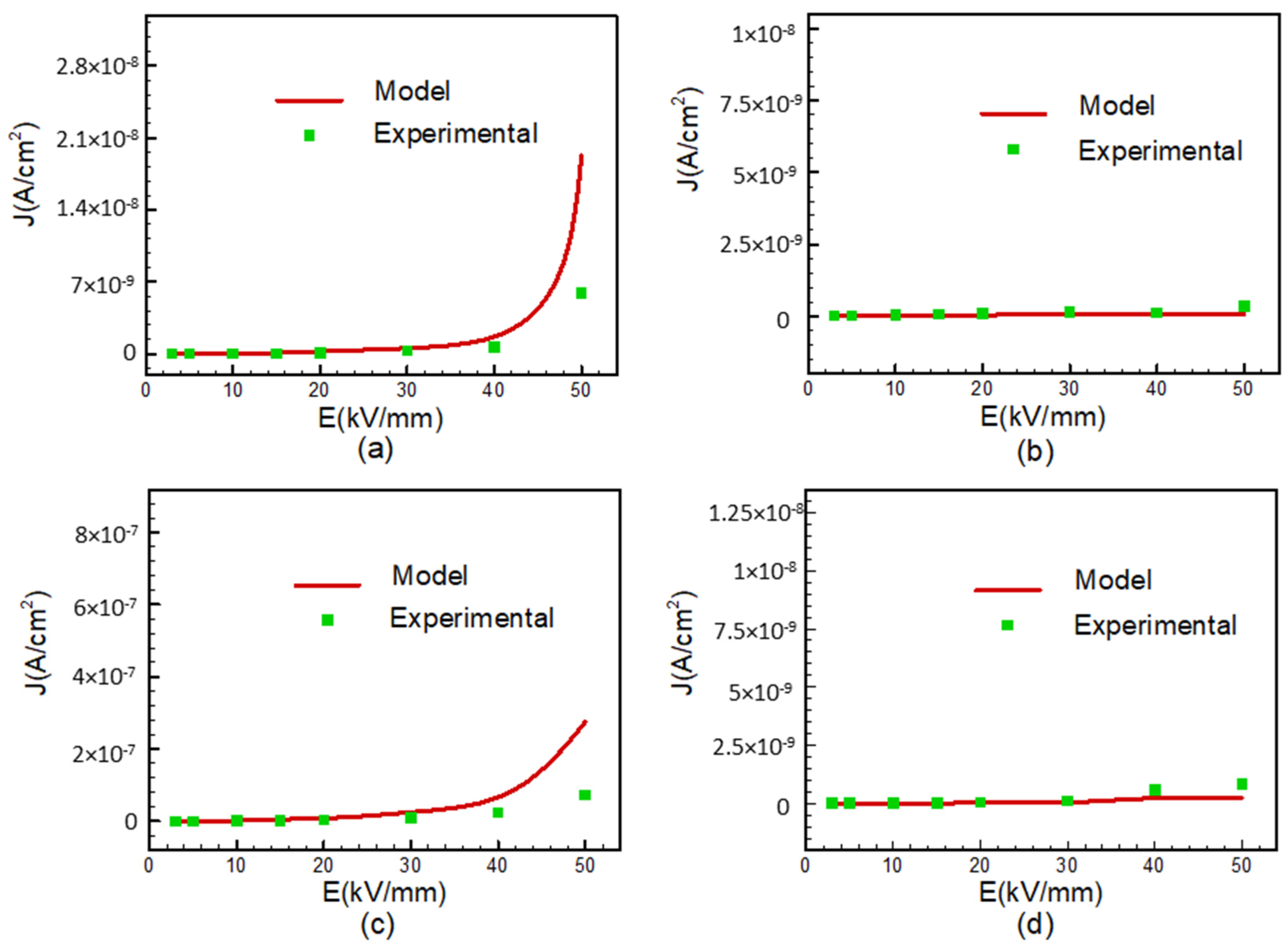
Polyimide plays a significant role in providing insulation for electric motor windings. However, it is susceptible to degradation due to thermal fluctuations and electrical stresses. In practical electric motor operation, temperatures can reach up to 150 °C, increasing the risk of premature breakdown, including the accumulation of space charges and other forms of electrical conduction within the material. Hence, this study aims to investigate the correlation between current density and electric field under varying temperatures, with the goal of yielding valuable insights applicable to electric motor systems in electric vehicles. The results are subjected to a comprehensive analysis aimed at identifying the prevailing injection or conduction mechanisms across all samples. Two prominent mechanisms were identified: Schottky injection and Poole–Frenkel barrier injection. Schottky injection occurs due to the activation energy barrier that electrons encounter at the junction between the electrodes and the dielectrics material, which results in a reduction of the energy barrier at this interface. Conversely, Poole–Frenkel emissions are associated with conduction of trapped electrons within the bulk of the insulating material. Such trapping electrons are able to acquire sufficient activation energy to de-trap and contribute to the overall conduction process. A further notable conduction phenomenon, capable of inducing nonlinearity (with a slope ≥ 2) in current density vs. electric field (J-E) plots, is space-charge-limited current (SCLC). The presence of traps within the material can exert an influence on the behavior of space-charge-limited current (SCLC). Consequently, these theoretical models can be effectively applied to interpret experimental findings and elucidate underlying conduction mechanisms. In a previous study, the results were assessed by employing various depictions of J in relation to E [
35,
36,
37]. When the data were presented on a log–log scale, it became apparent that in most samples, an ohmic current behavior was observed, characterized by a slope ≤ 1 in the low-field region denoted AB. However, upon reaching a threshold electric field, typically falling within the range of 10 to 15.5 kV/mm, contingent on temperatures condition, a notable nonlinear curve becomes evident in the graph, characterized by a slope exceeding 1. This nonohmic conduction behavior [
36] can be attributed to the SCLC regime. In this regime, the relationship between current density and electric field follows Equation (2) and is graphically represented in
Figure 5.
To ascertain SCLC conduction, it is imperative that the slope of the J vs. E
2/d curve equals 1. In
Figure 5, when the slope is less than 1 within the AB region, it points to an ohmic-dominant conduction mechanism, ruling out the possibility of SCLC being in effect.
A slope of 1 signifies trap-free SCLC, while a slope greater than 1 indicates SCLC with traps present. An examination of
Figure 5 reveals a slope equal to 1 for FPI and PI/SiO
2 samples at a temperature of 160 °C (with PI/SiO
2 showing a slightly better fit than FPI) [
28]. This confirmation of SCLC in this specific region reinforces the conclusion that the SCLC mechanism does not hold dominance in our samples under the examined conditions.
In summary, it appears that the space-charge-limited current (SCLC) phenomenon is only observable at 160 °C for FPI and PI/SiO
2 samples. However, when examining the second slope in the J–E curves for PI, FPI, PI/SiO
2, and PI-PI/SiO
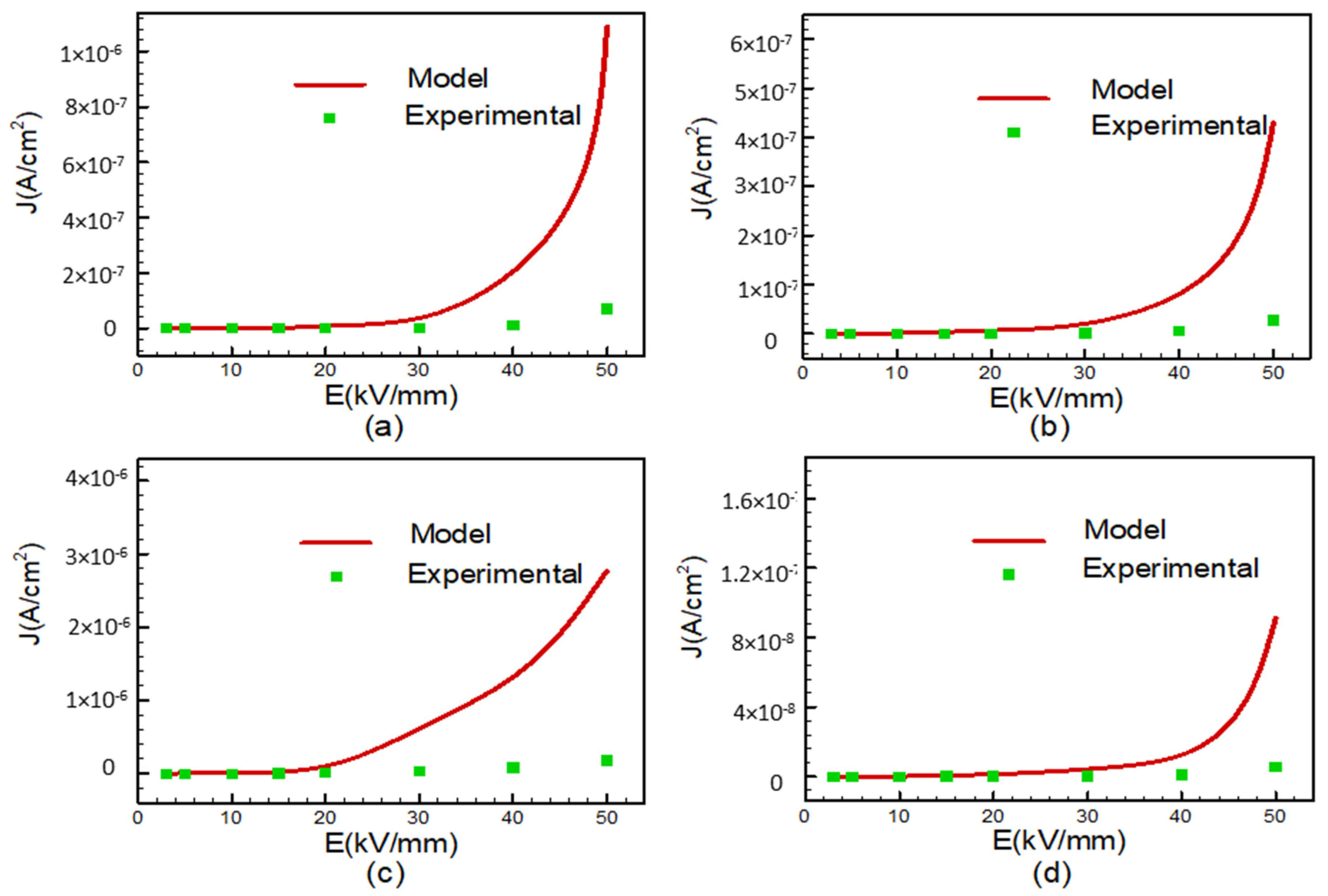
2 films subjected to higher E, it becomes evident that these slopes exhibit higher values, which could be indicative of either trap-filled regions or alternative conduction mechanisms. Specifically, the second slope for PI film at 55 °C and for PI and FPI films at high temperature (160 °C) surpasses a value of 2, suggesting the involvement of alternative conduction mechanisms. Regions BC, where the slopes exceed 2, defy explanation through the SCLC regime alone. It is plausible that the chemical and physical composition of the samples, particularly with respect to the glass transition, exert a significant influence on conduction in these regions. Consequently, the dominant conduction mechanisms observed in this area likely involve factors beyond SCLC. Additional conduction mechanisms, such as Schottky, Poole–Frenkel, and hopping conductions, need to be included in order to comprehensively understand the observed behaviors. The Poole–Frenkel effect, for instance, constitutes a bulk conduction mechanism in which the barrier between localized states is diminished under the influence of a high electric field, and this effect is characterized by Equation (3) [
36].
In the context of this analysis, let us consider the following parameters: σ
0 represents the intrinsic conductivity of the material, and β
PF is the Poole–Frenkel constant defined in Equation (4), with k representing the Boltzmann constant and T denoting the absolute temperature. When the Poole–Frenkel conduction mechanism takes precedence, it is expected that the plot of ln (J/E) versus E
1/2 will manifest as a linear relationship, with a slope closely approximating β
PF/(kT). The first step involves computing the β
PF coefficients based on the slope observed, followed by deriving estimates of dielectric constants using Equation (4). If these estimated dielectric constants align with values found in the established literature, it suggests that the samples conform to the associated conduction mechanism. We have illustrated these representations in the ln (J/E) versus E
1/2 coordinates in
Figure 6. Upon examination, these representations do not exhibit linearity for FPI, PI/SiO
2, and PI-PI/SiO
2 films at 55 °C, and their calculated dielectric constants fall within the range of 6 to 15. This range surpasses the measured values. Similarly, the slopes of these representations are non-linear for PI, FPI, and PI/SiO
2 films at 160 °C, with their calculated dielectric constants falling within the range of 0.8 to 2.2, which is below the measured values, as detailed in
Table 1. Consequently, it appears that Poole–Frenkel conduction is not the predominant mechanism for these films. However, notable exceptions include the linearity observed for PI at 50 °C, FPI, PI/SiO
2, and PI-PI/SiO
2 films at 110 °C, where the values closely approximate the calculated β
PF/(kT) values. Furthermore, this linear behavior extends to multilayer PI-PI/SiO
2 nanocomposite films at 160 °C, where the calculated dielectric constant closely aligns with the measured one. This alignment lends support to the presence of Poole–Frenkel conduction in these particular films. In cases wherein the Poole–Frenkel conduction mechanism is not observed in the films, it becomes imperative to explore alternative conduction pathways. Consequently, we turn our attention to the charge injection phenomenon, specifically Schottky injection, as a potential candidate for explaining conduction in these films. In the context of Schottky injection, the applied electric field serves to diminish the potential barriers, enabling electrons to surmount these barriers through a process often described as “jumping” [
28].
The current density resulting from the Schottky effect can be quantified using Equation (5), and its graphical representation can be found in
Figure 7.
In this context, let us introduce the key parameters involved. A
s represents the Richardson–Dushman constant, characterizing thermionic emission, while
signifies the potential barrier height at the metal–dielectric interface in the absence of any applied field. Additionally, β
S, defined in Equation (6), corresponds to the Schottky constant, and E
C pertains to the electric field at the cathode. Determining the precise electric field at the cathode during measurements can be challenging due to distortion caused by space charge effects. To address this, we propose the utilization of a parameter denoted as
, as outlined in Equation (7):
When
is less than 1, indicating a prevailing contact homocharge, and when
is greater than 1, indicating a prevailing contact heterocharge, the Schottky current expression is modified by the field distortion correction, as depicted in Equation (8):
We determined the
parameter by calculating it from the slope of the fitted curves, as depicted in
Figure 7, using Equation (9). With the knowledge of ε
r and the experimental slope,
can be computed, as summarized in
Table 2. Moreover, extending this straight-line analysis provides insight into the determination of
. Notably, higher
values indicate a pronounced influence of heterocharge near the cathode, which significantly augments the local electric field and tends to diminish the energy barrier at the interface.
Table 2 provides an overview of the experimental slope values, calculated β
S/kT values, measured and computed dielectric constants, as well as the derived
values for reference.
When evaluating the dominance of Schottky emission in conduction, it is expected that a plot of log (J) against E
1/2 will exhibit a proportional relationship, forming a linear curve in accordance with Equation (5). Initially, we calculate the β
S coefficients based on the slopes of the log (J) vs. E
1/2 plots. Subsequently, we estimate dielectric constants from these coefficients, employing Equation (6). The alignment of these calculated dielectric constants with measured values serves as an indicator of whether the samples adhere to the Schottky conduction mechanism.
Figure 7 reveals that only single and multilayer PI/SiO
2 films at 55 °C exhibit linear ln(J) vs. E
1/2 plots, with their slope values closely resembling β
S/kT values. Furthermore, the calculated dielectric constant values for these films closely match the measured values. Consequently, it is plausible that Schottky conduction may be a valid mechanism for these particular films. However, for other films, the ln(J) vs. E
1/2 plots deviate from linearity, and their calculated dielectric constants are notably lower than the measured ones. In fact, the dielectric constant values derived from the slopes in
Figure 7 fall below 1, which is not a tenable scenario. In contrast, measurements in
Table 2 and the available literature consistently report dielectric constants ranging from 3.6 to 4.0 [
36]. This stark disparity strongly suggests that the Schottky conduction mechanism is likely not applicable to all the films, except for PI/SiO
2 and PI-PI/SiO
2 films at 55 °C, which exhibit dielectric constants of 1.53 and 2.29, respectively. Hence, it becomes evident that Schottky conduction can be ruled out, pointing toward the presence of alternative conduction mechanisms, possibly involving hopping between trapping sites, in these films.
Ultimately, we can employ the concept of the hopping conduction model to elucidate the conduction process in the films that do not conform to alternative models. In hopping conduction in an electrical field, the barrier for ion transport is reduced by an electric field as in Equation (10), i.e., in an electrical field the energy that the ions require to transport (the energy barrier) is reduced by energy gained from the field in moving in the field direction. Thus, the ions gain energy from both electrical and thermal sources. Equation (10) allows us to express the current density, denoted J, through the framework of the ionic hopping conduction model [
35].
In this context, we introduce a set of vital parameters: e (electron charge), n (carrier density), α (hopping distance), ν (attempt to escape frequency), U (activation energy), k (Boltzmann constant), and T (absolute temperature). These parameters collectively govern the hopping conduction model. The hopping distance (α) can also be approximated by analyzing the slope of ln(J) vs. E plots, as presented in
Figure 8. To align the hopping conduction model with experimental data, we fine-tune constant parameters such as charge carrier density (n), hopping distance (α), and attempt-to-escape frequency (ν), as depicted in
Figure 9,
Figure 10 and
Figure 11. It is worth noting that these parameters are inherently material-specific, with polyimide being our primary material. Their estimation can be accomplished through experimental data and validated against existing literature [
10,
29]. Our findings indicate that the hopping distances for all samples fall within the range of 2.6 nm to 5 nm. This range exhibits slight variations due to factors such as temperature and material composition. To address this, two approaches are viable: we can define a specific range and select values based on temperature considerations, or alternatively, we can opt for a single value that accommodates all temperature conditions. It is important to note that these minor variations in value do not significantly impact the final calculation of current density. In our analysis, we have chosen a value that is most suitable for all the materials studied within the range of 2.6 to 5 nm, encompassing temperatures of 55 °C, 110 °C, and 160 °C. To ascertain the presence of hopping conduction in the films, the model-fitted curves must align closely with the experimental data. As observed in
Figure 9, FPI and PI-PI/SiO
2 films exhibit a strong curve fitting at 55 °C. However, at 110 °C, as seen in
Figure 10, no film demonstrates a satisfactory curve fit, thereby excluding the possibility of hopping conduction. At 160 °C, as depicted in
Figure 11, PI and FPI films exhibit the best data matching across the entire electric field range, confirming the occurrence of hopping conduction in these materials.
Table 3 below provides a comprehensive overview of potential conduction phenomena observed across all the materials investigated at various temperatures and within the considered electric field ranges. To describe the steady-state conduction current, it is essential for at least one conduction mechanism from each class, encompassing both charge injection and bulk conduction, to be present. However, some samples, such as FPI and PI-PI/SiO
2, appear to exhibit two different conduction mechanisms falling within the same bulk conduction category, especially at the elevated temperature of 160 °C, as depicted in
Table 3. For instance, in the case of FPI films at 160 °C, both space-charge-limited current (SCLC) and hopping conduction appear to coexist. SCLC is associated with the mobility of both holes and electrons, while hopping conduction involves ions at donor and acceptor sites within the bulk. These ions require either thermal or electrical energy to participate in conduction by making room for neighboring electrons or holes, depending on their respective trap energy levels. It is important to note that our estimation of these conduction phenomena is based on the analysis of current density slopes over specific electric field ranges, rather than at individual points. Therefore, it is challenging to precisely pinpoint the exact electric field in which these conduction mechanisms occur. Exploring conduction mechanisms in polymeric materials, particularly in the case of composite materials, presents a complex challenge. This complexity becomes even more pronounced in the context of this study. Our findings underscore that the dominant conduction mechanisms are significantly influenced by both the electric field strength and the measurement temperature, regardless of the specific material under examination. However, within the scope of this study involving polyimide-based materials, it is evident that two bulk conduction mechanisms, namely Poole–Frenkel and hopping, emerge as primary contributors, particularly at elevated temperatures of 110 °C and 160 °C.
The Poole–Frenkel effect and hopping conduction are two different mechanisms that describe the electrical behavior of insulating materials, including polymers. These mechanisms are often associated with the flow of charge carriers (usually electrons) through insulating materials, and they occur under different conditions and have distinct characteristics. Poole–Frenkel conduction is a mechanism that explains electrical conduction in insulating materials due to the presence of localized traps or defect states within the material’s bandgap. It occurs when charge carriers (usually electrons) are thermally excited from the valence band into these localized traps or defect states, where they can then move under the influence of an applied electric field. The Poole–Frenkel effect is highly temperature-dependent. As temperature increases, more charge carriers are thermally excited into the traps, resulting in an increase in conductivity. Hopping conduction is a mechanism that describes electrical conduction in insulating materials through a series of random, localized hopping events between neighboring sites or states. In hopping conduction, charge carriers move from one localized state to another by tunneling or hopping. This mechanism is usually more relevant at lower temperatures and in materials with a wide distribution of energy states. Hopping conduction is strongly temperature-dependent, and is often described by Mott’s variable-range hopping law. At low temperatures, the conductivity decreases exponentially with decreasing temperature. The energy gap of polyimides typically spans between 3 and 4 (eV) [
37]. The chemical structure of polyimide features both crystalline and amorphous regions. The amorphous structure extends the electron into the band gap, giving rise to localized energy levels below the conduction band for electrons and above the valence band for holes. Other chemical irregularities, such as structural imperfections and molecules (e.g., additives or impurities), introduce additional localized energy levels within the band gap. These energy levels, situated within the forbidden energy range, serve as capture sites for available charge carriers, thereby impeding charge transport. While electrons cannot be thermally excited to bridge the significant band gap, they can potentially surmount the potential barrier that separates local energy levels below the conduction band, thus facilitating electron transfer in polymers. Hole transport can similarly occur by surmounting the potential barrier between energy levels positioned just above the valence band. The specific mechanism, whether it involves hopping or tunneling, depends on the energy of excited electrons, the shape of the barrier’s height, and the separation between these energy levels. Both mechanisms collectively contribute to the bulk conduction behavior of polymers. In situations where a series of single-level trap sites, each with an energy level denoted
, are located within the band gap of polymers, trapped electrons have the ability to leap over the potential barrier. The probability of electron hopping per unit of time can be described using Equation (11). Where
v is the escape velocity in the range of of 10
11 to 10
14 per second;
kB is the Boltzmann constant and
T is the temperature.
Electrons confined within localized states also possess the capability to transfer and migrate into the conduction band of insulators. This occurrence can be attributed to an internal Schottky effect (Equation (12)), where the potential barrier height due to the Coulombic force generated by positively charged ionic centers is reduced by high electric fields. Importantly, the Coulombic force in the Poole–Frenkel effect (Equation (13)) stems from a stationary positive charge, whereas in the Schottky effect, it results from a movable image charge. Consequently, the potential barrier reduction in the Poole–Frenkel effect is twice as substantial as what is observed in the Schottky effect [
38]:
where
βSch is called the Schottky constant and
βPF is the Poole–Frenkel constant. Consequently, the conductivity due to the Poole–Frenkel effect in the bulk of insulators can be expressed as Equation (14), in which the Poole–Frenkel conductivity is expressed as a function of the Schottky beta function.


