Article

An Overview of Strengths and Weaknesses in Using MOSFET Experience for Modeling GaN HEMT

by
Enrico Alfredo Bottaro
and
Santi Agatino Rizzo
*
Department of Electrical Electronic and Computer Engineering (DIEEI), University of Catania, 95125 Catania, Italy
*
Author to whom correspondence should be addressed.
Energies 2023, 16(18), 6574; https://doi.org/10.3390/en16186574
Submission received: 18 July 2023 / Revised: 31 August 2023 / Accepted: 8 September 2023 / Published: 12 September 2023

Abstract

:
GaN high electron mobility transistors (HEMTs) represent an emerging and key enabling technology for obtaining highly efficient and compact power electronic systems. The use of circuit models of power devices is essential for the optimal design of power converters, but while they have been deeply investigated for power MOSFETs and IGBTs, GaN HEMT models are still in their early stages. This paper first discusses the main similarities and differences between conventional MOSFETs and GaN HEMTs in terms of the datasheet information that the device manufacturers use to obtain the behavioral models that they usually provide as Spice-like netlists. Then, it highlights the strengths and weaknesses of using the behavioral models of MOSFET for GaN HEMT. To achieve this aim, a study of the existing GaN HEMT models revealed the lack of a proper modeling strategy for the dynamic conduction resistance, which is the most critical aspect of HEMT modeling. The difficulty is due to the dependence of the dynamic conduction resistance on quantities related to the application, which is a behavior absent in power MOSFETs. Consequently, future research efforts on GaN HEMT modeling must face this issue.

1. Introduction

The high demand for highly efficient and compact power electronic systems in many applications is pushing towards a wide diffusion of wide-bandgap devices [1,2]. In applications above 600 V, the replacement of IGBTs with SiC MOSFETs provides several advantages thanks to their low conduction and switching losses that enable low working temperatures [2,3,4], thus increasing the lifetime and performance of the overall converter [5,6], and reducing heatsink requirements. In applications below 600 V, while silicon MOSFETs dominate the market, there is an increasing interest in and diffusion of GaN high electron mobility transistors (HEMTs) [7]. In fact, they have lower conduction losses, especially at high junction temperatures (Tj) [8]. Moreover, they present lower parasitic capacitances and lack the reverse current phenomenon, thus enabling very high switching operations that, in turn, lead to a significant increase in the power density [9]. Therefore, GaN HEMTs are very promising devices, provided that the benefits and limits of the current technology are properly considered during converter design [10].
It is widely recognized that in converter design, it is very important to use circuit models of the power devices. Moreover, it is necessary to properly model the behavior of the driver and control circuitry. Finally, it is also essential to evaluate the parasitic inductances of both the device and the whole system and use them during the circuit simulation to foresee the time-domain waveforms.
The main contribution of this paper is proposing and proving that behavioral models (or physics/semi-physics models treated as behavioral ones) of Si and SiC MOSFETs can be successfully used for GaN HEMT modeling. Moreover, because GaN HEMTs present some specific features, such as dynamic conduction resistance (RDS,on) the limits of this strategy are also highlighted. Section 2 gives a brief overview of the advantages and limitations of different device modeling approaches. Section 3 analyzes the main similarities and differences between MOSFETs and GaN HEMTs, considering in detail the datasheet information necessary to obtain netlists that can be simulated using Spice-like software. Section 4 presents an overview of the GaN models proposed so far.
This study has confirmed the poor availability of GaN HEMT models and their limits. Such an overview is twice as useful. It has enabled the validation of the comparison reported in Section 3 and, consequently, the overview confirms that the use of behavioral models of MOSFETs is a good practice for GaN HEMT modeling. The overview is also useful for developing new and accurate models. In fact, the analysis in Section 5 pinpoints the main limits of the existing models that hinder accurately emulating the static and dynamic behavior of these devices. More specifically, the analysis highlights that future research in GaN circuit modeling must focus on proper modeling of the dynamic RDS,on and parasitic output capacitance.

2. Power Electronics Devices Modeling

Physics models enable us to accurately analyze the functioning of the devices since they account for the physical structure of the devices [11,12]. Then the physical phenomena inside the device are modeled, such as the phenomenon of trapping and de-trapping of the charges [13]. Some physics models can only be simulated using tools based on the finite element method [14]. Other models use mathematical functions that include parameters related to the physics of the device quantities, which are sometimes also evaluated by adopting finite element simulations [15]. The latter can be implemented in netlists used for circuit simulations. A negative aspect related to all the aforementioned models is that they require knowledge of the device structure, materials, doping, fabrication processes, connections, and so on. Power converter designers do not have this information since it is “proprietary” and, obviously, not provided by device manufacturers.
“Time-segmented” analytical models use different sub-models of the device based on the different working operations of the device and circuit over time. In each time interval, the waveforms are evaluated by numerical simulation of a differential equation system obtained by combining Kirchhoff laws and branch equations, both of which vary as the device submodel and circuit change [16,17]. An advantage of “time-segmented” analytical models is that they avoid the aforesaid information (device structure and so on) while maintaining good accuracy. On the other hand, a disadvantage is that they analyze the different time intervals of the device’s functioning. Thus, for each subperiod, “time-segmented” analytical models require that the designer properly adapt the equations in order to account for both the devices and the topology of the power converters. To perform this task, the designer should consider all the equations involved in the equivalent circuit related to the devices and their interconnections, as well as the connections with the power supplies, loads, drivers, and so on. Consequently, “time-segmented” analytical models are unlike for the designers, considering that it is necessary to implement analytical equations in proper computing software to obtain the waveforms of the desired quantities.
Behavioral models treat the device as a black box because they need information usually reported in the datasheet to obtain the values of the parameters of the mathematical functions implemented in the model itself without the need for previous information (device structure and so on). More specifically, these fitting parameters are properly set to obtain simulation quantities and waveforms compliant with datasheets and laboratory measurements [18]. Therefore, device manufacturers provide a behavioral model that reflects a “typical device” according to the datasheet characteristics [19].
Semi-physics models combine mathematical functions based on device physics with behavioral parameters. More specifically, semi-physics models include few behavioral parameters in the mathematical functions based on the device physics, aiming at improving accuracy without increasing the simulation effort [20].
Device manufacturers usually provide Spice-like netlists implementing their own behavioral or semi-physical models. The use of these kinds of models is a common approach in industry, and it is also widely adopted in academia. It is worth noticing that only behavioral models have the advantage of being totally independent of proprietary information. However, physics or semi-physics models turn into behavioral ones when all their function parameters are treated as fitting parameters regardless of the original value of the related physics quantities. An effective example of this approach is reported in [21], where it has been proved that its proposed physics model can be characterized from a commercial datasheet without knowledge of the device structure, materials, doping, fabrication processes, connections, and so on. The optimal design of a power converter requires accurate circuit models of the power device that encompass the mutual interaction of thermal and electrical quantities [22]. On the other hand, low computational effort, especially fast simulation, is also important, so the optimal trade-off is highly desired [20]. The high computational cost of physics models does not enable them to reach this target. Finally, obtaining quickly a circuit model endowed with all the previous features is an important additional target for manufacturers to reduce the development cost [23].
It is worth noticing that when a new MOSFET device is industrialized, it is not necessary to develop a new behavioral model. Considering that the shapes of the static and dynamic characteristics of different MOSFETs are similar regardless of their magnitude. Therefore, the adoption of available models that already present a good trade-off in terms of accuracy and simulation time is the best approach to reducing the model development cost: workers involved, software and hardware necessary, development time to provide the model to the customers, and so on. The adoption of available models implies that the modeler has only to find among them the one providing the optimal trade-off for the new device. The task is easily performed by using an optimization algorithm to find the optimal fitting parameter values for the mathematical functions of each model. After that, these models can be compared in terms of accuracy and simulation effort to select the best one. From this perspective, this paper proves that this approach is also an interesting strategy for developing appropriate circuit models for GaN HEMT. More specifically, the exploitation of the black-box approach typical of behavioral models enables the adoption of models that already satisfy these conflicting targets (good accuracy, fast simulation, fast development of models) for well-established devices, thus strongly reducing the model development cost. In fact, while only a few circuit models of GaN are available, there is a large number of Si and SiC MOSFET models that have all the aforesaid good features and could be adapted for GaN modeling. Therefore, in the following, the paper will focus only on behavioral models or physics/semi-physics models treated as behavioral ones. This approach enables the use of the GaN HEMT of physics/semi-physics models developed for Si and SiC MOSFETs, although these devices present different structures, materials, physics features, and so on.

3. Comparison between MOSFET and GaN HEMT

Behavioral models are based on a black-box approach that exploits information at the device terminals, as the one reported in the datasheet, in terms of static and dynamic characteristics. This section describes the main similarities and differences among Si, SiC MOSFETs, and GaN HEMTs in terms of static and dynamic characteristics as reported in their datasheets. This comparison is necessary to identify the MOSFETs’ modeling approaches that are suitable for GaN HEMTs and the new modeling strategies necessary to account for the differences. It is worth mentioning that only the shapes of the characteristics are compared while the magnitude is neglected since the behavioral models are based on mathematical functions whose parameters can be proportionally tuned to account for the different magnitudes. In other words, the key aspect is the use of mathematical functions able to approximate a given characteristic shape. For instance, functions better at accounting for different transitions between different operating regions would be widely used. Similarly, a more accurate simulation can be carried out when the models are improved by tuning the fitting parameters according to the specific devices used in the converter.
The study considers commercially available devices with breakdown voltage ratings of 600 V or 650 V. However, according to the previous discussion, the basic ideas and considerations are general and can be extended to different voltage ratings. The comparison has been performed by considering characteristics that are usually adopted for obtaining accurate circuit models, as summarized in the following paragraphs. Table 1 reports the devices used to better clarify the analyses. Different devices have been considered to underline the generality of the analyses.
(A)
Output Characteristic (OC) expressed in terms of drain current, ID, vs. drain-source voltage, VDS. Figure 1A shows typical output characteristics of Si MOSFET (Tj = 125 °C, VGS = 10 V), SiC MOSFET (Tj = 175 °C, VGS = 20 V) and GaN HEMT (Tj = 150 °C, VGS = 4 V).
  • Dissimilarity—None in terms of shape.
  • Similarity—The shape of the curves is analogous.
(B)
Transfer Characteristic (TC, ID vs. gate-source voltage, VGS)—Figure 1B shows typical transfer characteristics of Si MOSFET, SiC MOSFET, and GaN HEMT at ambient temperature (Tj = 25 °C) and Tj = 150 °C.
  • Dissimilarity—When the MOSFET is considered, the effect of the temperature on ID depends on VGS. The drain currents of Si and SiC MOSFETs are independent of Tj for a specific VGS, known as the zero temperature coefficient (ZTC) point (see Figure 1B). Another difference is the behavior of the MOSFET below the ZTC point, where ID increases with Tj. There is not any ZTC point in GaN HEMT, and ID never increases with increasing Tj. The shape of the GaN HEMT curve (blue in Figure 1B) is different from the MOSFET’s one.
  • Similarity—In MOSFETs and GaN HEMTs, ID increases with VGS at any temperature. Above ZTC, the MOSFET current decreases with increasing Tj. This behavior also occurs in GaN HEMT, whatever the VGS.
(C)
Threshold Voltage (VTH, VTH vs. Tj)—Figure 1C shows typical trends of the threshold voltage for increasing junction temperature.
  • Dissimilarity—In Si and SiC MOSFETs, VTH decreases with increasing Tj, while GaN HEMT presents a temperature-independent threshold.
  • Similarity—None.
Figure 1. Comparison among Si, SiC MOSFET, and GaN HEMT. The datasheet is the data source. (A) Output characteristic (B) Transfer characteristic (C) Threshold voltage (D) Conduction resistance (E) Third-quadrant (F) COSS.
Energies 16 06574 g001
(D)
Conduction Resistance (RDS,on, normalized on-state resistance vs. Tj). Figure 1D shows typical curves for MOSFETs and GaN HEMTs.
  • Dissimilarity—SiC MOSFET presents a “U-shape” curve, then, below the room temperature, the conduction resistance decreases with increasing temperature, while in GaN HEMT the resistance always increases when the temperature increases.
  • Similarity—The curves of Si MOSFETs and GaN HEMTs are analogous, whatever the temperature. The curves of SiC MOSFETs and GaN HEMTs are analogous above room temperature.
(E)
Third-Quadrant (TQ, ID flowing in opposite direction vs. negative VDS). The physical structure of Si and SiC MOSFETs presents a parasitic diode that enables third-quadrant operations, but it introduces issues, especially in Si MOSFETs, related to the reverse recovery current.
  • Dissimilarity—GaN HEMT does not present any reverse recovery current thanks to the absence of a parasitic diode.
  • Similarity—MOSFETs and GaN HEMTs present analogous curve shapes of the third quadrant current (Figure 1E).
(F)
Parasitic Capacitances (CISS, CRSS, COSS vs. VDS). Any technology presents parasitic capacitance, although the GaN HEMT capacitance is widely lower than in MOSFET technologies, as shown in Figure 1F.
  • Dissimilarity—None in terms of shape.
  • Similarity—The shape is analogous.

4. GaN HEMT Circuit Models

This section analyzes the existing circuit models of GaN HEMTs, intending to confirm that the use of circuit models of MOSFETs is a good practice for modeling GaN HEMT devices. Therefore, MOSFET models successfully adopted for GaN and vice versa are mainly reported. Other GaN models, not adopted for MOSFETs, are analyzed based on the discussion in Section 3 for confirmation purposes too. Finally, Si and SiC MOSFET models that have not been used so far for GaN are not considered since they are not useful for the aim of this section, regardless of whether they could be successfully used for GaN modeling according to the discussion in Section 3.
Some of the following functions contain physical parameters related to a specific device’s material, structure, and so on. Therefore, they were originally used in physics or semiphysics models. When these functions are adopted for other kinds of devices, the original models are turned into behavioral ones since the physical parameters are treated as fitting parameters and lose any relation to the (different) device physics.
Figure 2 shows a typical representation of the component. The blocks named GMOS, RVAR, and third quadrant emulate the static characteristics of the device; the CGS, CGD, and CDS blocks, instead, emulate the dynamic ones. The current IGMOS is set using the equation implemented in the GMOS block. The equations implemented on these blocks usually include some fitting parameters properly set to obtain a good match between the datasheet characteristics and the simulated ones.

4.1. GMOS

This block represents the core of the device since it emulates the OC and TC. The following model, developed for MOSFET devices [24], has been successfully used for GaN HEMT. More specifically, MOSFET “level 3” equations have been used for modeling the GaN HEMT [25]:
I G M O S = K n 1 + θ V G S V T H W L V G S V T H V D S R s I D R d I D 1 + γ 2 ρ V D S R s I D R d I D 2 2 Triode   region K n 1 + θ V G S V T H W L V G S V T H 2 ρ ρ + γ Saturation   region
where Kn is the transconductance, Rs is the source resistance, Rd is the drain resistance, γ is the body-effect parameter, ρ is the surface potential in strong inversion, θ the mobility modulation constant, and L and W are, respectively, the channel length and width. A method for extracting the value of previous parameters is proposed in [25]. These MOSFET equations have been used in the GMOS block of two GaN HEMT devices manufactured by GaNSystem. As pointed out before, any physical parameter is processed as a fitting parameter. Figure 3 reports one of these comparisons between the OC and TC simulated by adopting the values of the parameters proposed in [25] and the target ones. Although the results are almost good, they were obtained at room temperature only, so the current variation with Tj is not considered. Therefore, according to the consideration for the OC, it has been easy to adopt the MOSFET “level 3” equations for GaN HEMTs, while they are not useful for the TC due to the dissimilarities related to ZTC as discussed in Section 3 at point B.
The accuracy of the models related to (1) and (3)–(20) that will be discussed in the following has been tested similarly to the comparison reported in Figure 3. The tests were performed when there was enough information in the original papers to execute the simulations. Then the error has been computed:
E r r o r = E r r p N P % = s i m u l a t e d p t a r g e t p t a r g e t p N P %
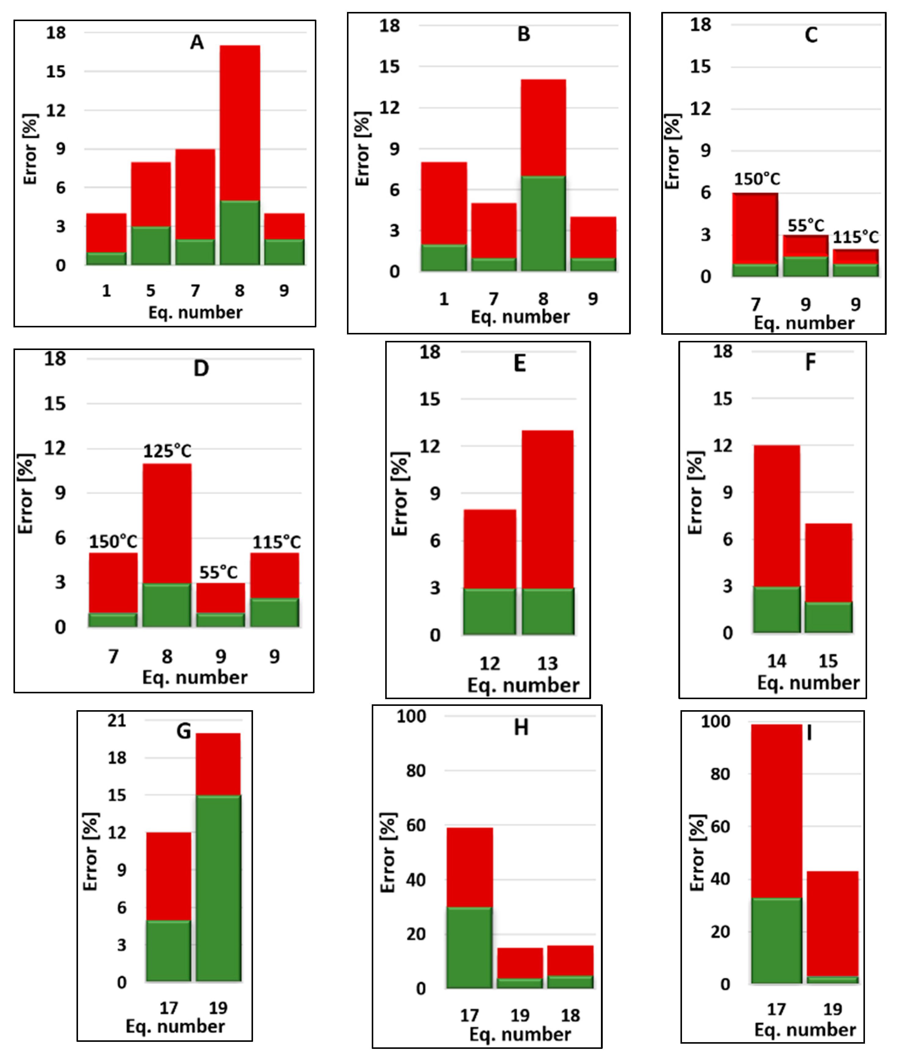
where the target is: the published measurement data when available in the original paper; otherwise, the datasheet information (p indicates the p-th point in the characteristic curve; NP is the number of points). Figure 4 shows the computed average (computed using (2)) and maximum (maximum value of Errp) errors. Each bar represents the percent error obtained for the labeled equations (x-axis). The bars related to the maximum error (red) are located behind the ones related to the average (green) value. For example, the label “1” in Figure 4A represents the use of Equation (1) for the device whose simulated and target curves are reported in Figure 3A. The related bars show the average (1%) and maximum (4%) error between the simulated and target curves computed by using (2).
The following models have been developed for HEMT devices; after that, they have been successfully used for SiC MOSFETs. The models based on the Curtice one [26] achieve excellent results for GaN HEMT and SiC MOSFET [27] when implemented in the GMOS:
I G M O S = b 1 + λ · tanh a V D S · 1 + λ 1 + 1 1 + λ 1 1 e V D S V T
where λ′, VT, a, and b are fitting parameters. In terms of OC and TC, the results claimed in [27] are very satisfying. The Angelov model developed for the RF HEMT device [28] has been used for the SiC MOSFET model in [29,30]. The original Angelov equation model is:
I G M O S = K n 1 + t a n h ψ 1 + λ V D S t a n h α V D S
where: ψ = P 1 V G S V p k + P 2 V G S V p k 2 + P 3 V G S V p k 3 and α is the saturation voltage. λ is the channel length modulation, and Vpk is the gate voltage at the maximum transconductance. P1, P2, and P3 are fitting parameters. Once again, the equation does not account for the dependence of the current on the Tj, so it can be used for both technologies. Therefore, the successful adoption in the GMOS block of MOSFET models for GaN HEMTs and vice versa confirms the usefulness of exploiting the wide MOSFET circuit modeling experience for developing the GMOS block when the temperature variation can be neglected. Another GaN HEMT model of the GMOS that does not account for the dependence on temperature has been developed by GaNSystem [31]:
I G M O S = a · log 1 + e b 1 V G S c · V D S 1 + max d + e V G S + f 1 , 0.2 · V D S V D S 0 0 V D S < 0
where a, b1, c, d, e, and f1 are fitting parameters. According to Figure 4A, the maximum error between the simulated and target curves in the output characteristic is about 7%, while the average error is about 3%. This confirms the achievement of a satisfactory result.
In the following, the temperature-dependent models of the GMOS proposed so far for GaN HEMT devices are discussed. The models are reported in increasing order of complexity. In particular, [32] has proposed a GMOS block that contains two equations. The first equation models the linear region, and the second equation emulates the saturation region:
I G M O S = K n 1 + T C 1 T j 25 + T C 2 T j 25 2 · V G S V T H V D S V D S 2 2 V D S < V G S V T H K n 1 + T C 1 T j 25 + T C 2 T j 25 2 · V G S V T H 2 1 + λ 1 V D S 2 V D S > V G S V T h 1 0 V D S < 0  
where TC1 and TC2 are fitting parameters. The results reported in [32] are unsatisfactory. Another model that contains few fitting parameters has been proposed in [33]:
I G M O S = A C V G M O S S S · V G S + tanh V G M O S · log 1 + e 3 V G S T H · 1 B T j 25
where AC, SS, TH, and B are fitting parameters. According to Figure 4A,B, the simulated OC and TC using (7) are in good agreement with the target curves (low average error), although a portion of the simulated characteristic presents a non-negligible difference with the target curve. Even at high temperatures (Figure 4C,D), the model presents a very good average error, while the maximum one is acceptable. By increasing the complexity of the models, the one proposed in [34] is reported. The OC and TC are emulated through the following equation:
I G M O S = K 1 1 l 1 T j 25 · ln 1 + e V G S b 1 c 1 · m 1 + n 1 V G S V D S 1 + 1 h 1 T j 25 d 1 + e 1 V G S V D S V D S > 0 0 V D S < 0
where K1, m1, n1, d1, e1, l1, h1, b1, and c1 are fitting parameters. The results, as shown in Figure 4A–D, are few satisfactory. The work [35] has proposed a modification of the temperature-dependent term of the previous equation, introducing a quadratic function:
I G M O S = K 1 1 + T C 1 T j 25 + T C 2 T j 25 2 · ln 1 + e V G S b 1 c 1 m 1 + n 1 V G S V D S 1 + 1 h 1 T j 25 d 1 + e 1 V G S V D S V D S > 0 0 V D S < 0
where TC1, TC2, K1, m1, n1, d1, e1, h1, b1, and c1 are fitting parameters. According to Figure 4A–D, (9) is the best model in terms of accuracy. Another equation, developed by GaNSystem, is reported in [36]:
I G M O S = k 1 k 2 + k 3 T j 25 log 1 + e k 4 V G S k 5 k 6 · V D S 1 + max k 7 + k 8 V G S , k 9 V D S
where k1–k9 are fitting parameters. In terms of TC, the results claimed in [27] are not good enough. The most complex equation is the following: It contains 12 fitting parameters and is based on a model developed by EPC [37]:
I G M O S = k 1 1 k 2 T j + k 3 V D S V G S + k 4 k 5 · · 1 e k 6 1 k 7 T j + k 3 V D S V G S + k 4 k 5 V D S · · V G S V T H + k 8 k 9 V G S V T H k 10 k 11 k 12 · 1 + tanh 10 3 V D S 1 tanh 10 3 V G S V T H
where k112 are fitting parameters.
The behavior of the GaN HEMT is different from that of the MOSFET at varying temperatures. In fact, (6), (7), (10), and (11) are not adaptable to MOSFETs because the temperature-dependent term is a multiplicative factor in the IGMOS equation that decreases with increasing temperature. Therefore, this term emulates a decreasing IGMOS with increasing temperature, regardless of the value of VGS. On the other hand, (8) and (9) could be used in MOSFET models because an appropriate combination of the fitting parameters could allow emulating the ZTC. The analysis reveals that such kinds of equations can emulate the ZTC of the MOSFET and at the same time be used for GaN since they set the ZTC at VGS equal to the VTH for the GaN HEMT (Figure 1B).
Therefore, the interesting aspect that emerged from this analysis and discussion is that any equation used for the MOSFETs can be adaptable for the GaN if the equation enables setting the GaN HEMT ZTC at VGS equal to the VTH. This approach makes it easier for GaN manufacturers to quickly develop a GMOS model endowed with a good trade-off between accuracy and simulation speed.

4.2. RVAR

The RVAR block accounts for the conduction resistance characteristic, RDS,on, then in this block is implemented a temperature-dependent equation. More specifically, this block interacts with the others (mainly the GMOS) to set and emulate the temperature-dependent RDS,on. There are circuit models that lack an RVAR block because RDS,on is incorporated into the GMOS equation [30].
A very limited number of equations have been proposed so far for GaN HEMT. They are reported in the following order of increasing complexity: A behavioral RVAR equation is proposed in [33]:
R V A R = S L T j 25 S L T · I D · V G S · 1 + A T J 25
where SL, SLT, and A are fitting parameters. GaNSystem uses an RVAR block implemented through a voltage source whose equation is [38]:
R V A R = I D · A · B 1 C T j 25 + D T j + 273 298 E 5 e 3
where A, B, C, D, and E are fitting parameters.
According to Figure 4E, (12) and (13) enable a sufficient average error, but the maximum is not negligible, especially for (13). In this case, there is no MOSFET model of RVAR used for GaN HEMT. However, according to the comparison performed in Section 3, these RVAR equations developed for GaN HEMT are usable for SiC MOSFET for the range of temperatures over 25 °C, while they are usable for Si MOSFET at any temperature. Therefore, any conduction model developed for Si MOSFET can be adapted for GaN HEMTs, while only the conduction models developed for SiC MOSFET from room temperature upwards can be useful for GaN HEMTs. This enables the modellers to use, for the RVAR block, the MOSFET model that better fits with their GaN.

4.3. Third-Quadrant Conduction

This block emulates the TQ drain current. Only the following equations have been proposed for GaN HEMT so far. A model without any temperature-dependence term that emulates the TQ current has been developed by GaNSystem [31]:
I T Q = 0 V d s 0 a · log 1 + e b 2 V G S V D S c · V D S 1 max d + e V G S V D S + f 2 , 0.2 · V D S V d s < 0
where a, b2, c, d, e, and f2 are fitting parameters. In the following, temperature-dependent models are reported. The work presented in [34] has proposed the following equation to simulate the TQ current:
I T Q = 0 V D S > 0 K 2 1 l 2 T j 25 · ln 1 + e V G D b 2 c 2 V S D 1 + 1 h 2 T j 25 V S D V D S < 0
where K2, m2, n2, d2, e2, l2, h2, and c2 are fitting parameters. According to Figure 4F, (14) and (15) enable a sufficient average error, but the maximum is not negligible, especially for (14). A more complex set of temperature-dependent equations contained in the TQ block has been proposed in [32] that has adopted a lower number of fitting parameters:
I T Q = 0 V D S > 0 K n 1 + T C 1 T j 25 + T C 2 T j 25 2 · V G D V T H , R V S D V S D 2 2 V S D < V G D V T H 2 K n 1 + T C 1 T j 25 + T C 2 T j 25 2 V G D V T H , R 2 2 V S D > V G D V T H 2
where TC1, TC2 are fitting parameters, and VTH,R is the threshold voltage for reverse channel conduction. The results reported in [32] are a little satisfactory. Differently from the previous approaches, the TQ current can be emulated through (3), implemented in the GMOS block [27]. In other words, the GMOS can concurrently emulate the OC, TC, and TQ while also obtaining a high accuracy level. This approach can also be adopted for GaN HEMT modeling.
According to this successful adoption in both MOSFETs and GaN HEMTs, as well as according to the considerations about the TQ reported in Section 3, it is useful for developing the TQ block of GaN HEMT through the exploitation of the MOSFET circuit modeling experience.

4.4. Parasitic Capacitance

Firstly, the models of the parasitic capacitances of MOSFETs applied to GaN HEMT are reported. In detail, [25,32] have modeled the parasitic capacitances through the p-n junction capacitance equation adopted in MOSFET models:
C D S = C d s o 1 + V D S V b i M
where Cds(0) is the zero-bias capacitance, Vbi is the built-in voltage, and M is the gradient coefficient. Function (17) models the capacitance characteristics with unsatisfactory results, according to Figure 4G–I.
The following equations are based on functions reported in order of complexity. In [39], two equations for CGD and CDS have been proposed:
C G D = a 1 1 + e b 1 V G D + c 1 + d 1 C D S = a 2 1 + e b 2 V S D + c 2 + d 2 a 1 1 + e b 1 V G D + c 1 + d 1
where a1–d1, a2–d2 are fitting parameters. According to Figure 4H, (18) enables a satisfactory average error, but the maximum is not negligible. In [31], a more complex equation that contains three hyperbolic tangent functions and 10 fitting parameters has been presented:
C G S = a 1 b 1 1 + tanh c 1 V G S + d 1 e 1 1 + tanh f 1 V G S + g 1 + h 1 1 + tanh i 1 V G S + j 1
where a1–j1 are fitting parameters. The same equation is used for CGD and CDS modeling. According to Figure 4G,H, the results are a little satisfactory for CGS and CDS. The results are even worse for CGD, according to Figure 4I. The last reported equation is developed by GaNSystem [36]:
C D S = k 1 log 1 + e k 2 V D S k 3 k 4 + k 5 log 1 + e k 6 V D S k 7 k 8
where k1–k8 are fitting parameters. The same approach is used for modeling CGS and CGD.
Therefore, although there is a limited number of modeling approaches proposed for the parasitic capacitance of GaN HEMTs, as highlighted in Section 3, the similarity of the curve trends of MOSFETs and GaN HEMTs enables the use of the circuit model of MOSFET capacitance for GaN HEMTs.

5. Problems in GaN HEMT Modeling

Circuit models have to provide accurate results with fast simulations. An important additional target for manufacturers is developing these models quickly. According to the analyses in Section 3 and Section 4, the use of MOSFET models to reach these targets has the following strengths: The approaches used for modeling the OC and TC of MOSFET can be easily adapted to GaN HEMT models by using the approach proposed in Section 4 to handle the MOSFET ZTC when the GMOS of the GaN HEMT has to be obtained. Regarding the static RDS,on, all the models used for Si MOSFET and some models used for SiC MOSFET can be used for GaN HEMT modeling. Finally, the comparison and the literature analyses have highlighted that the exploitation of the MOSFET modeling experience is useful for modeling the TQ and small-signal capacitance blocks of GaN HEMT.
On the other hand, there are some weaknesses to such an approach. GaN HEMT presents the current collapse phenomenon that must be taken into account in the circuit model, but if this phenomenon is absent in MOSFET, then there is no previous modeling experience that can be exploited. Moreover, recent studies have highlighted that the use of the datasheet information for modeling the output parasitic capacitance of MOSFETs and GaN HEMTs can lead to misleading simulation results, especially in high-frequency soft-switching applications. Although this phenomenon is also present in MOSFETs, it has only been discovered recently, so it has not been considered in MOSFET circuit models so far. Consequently, in this case, there is no previous modeling experience that can be exploited for GaN HEMT. In the following, these key problems in GaN HEMT modeling have been investigated.

5.1. On-State Power Loss

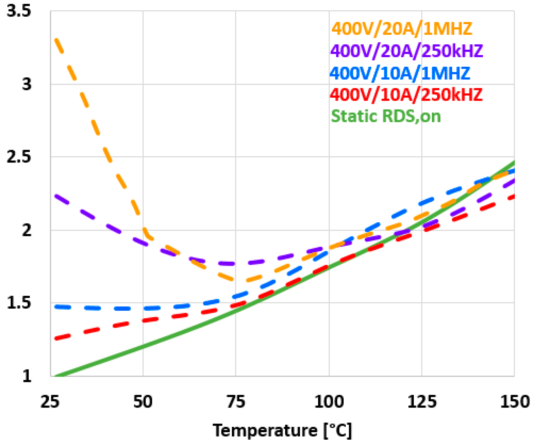
One of the most important problems with GaN HEMTs is the current collapse phenomenon, more commonly known as dynamic RDS,on. The current collapse phenomenon is due to some charges released into the 2DEG channel during the turn-on. These charges, previously trapped due to two trapping mechanisms, increase the conduction resistance and, consequently, the conduction losses [40]. A trapping mechanism occurs during the off state, and it is due to the blocked voltage. More specifically, the charges are trapped due to the high electric field across the device during the off-time [41]. The concurrent high current and voltage during hard switching provide enough energy for some electrons in the 2DEG channel to be trapped, thus introducing another trapping mechanism [42]. Several operating factors affect the dynamic RDS,on. In fact, it varies according to the application where the device is used. Dynamic RDS,on worsens (increases) with increasing the off-state voltage and off-time [43]. It also increases power applications at high frequencies, currents, and temperatures [44,45]. Figure 5 reports an example of a variation of the dynamic RDS,on with varying temperatures for different operating conditions as well as the trend of the static RDS,on [46].
The values are normalized with respect to the static RDS,on evaluated at room temperature. This phenomenon is almost absent in MOSFET, so there is not any previous modeling experience that can be transferred from MOSFET to GaN HEMT [47]. In other words, the use of the equations related to the RVAR block emulates only the dependence on the temperature. While the different trends in different operating conditions (Figure 5) highlight that a new function is necessary to emulate the behavior of the dynamic RDS,on, with varying temperature in order to account for the other operating conditions.
Dynamic RDS,on has not been fully taken into account in the circuit model of GaN HEMT, but it is of extreme importance to improve its accuracy. A first modeling approach for the dynamic RDS,on is reported in [43], but it only accounts for the off-state voltage and off-time. In such a work, the variation of the static RDS,on with varying VGS is first measured. Moreover, the device’s dynamic RDS,on is characterized by varying the aforementioned off-state quantities. Then, the circuit model (Figure 6a) emulates the dynamic RDS,on by varying the static one by, in turn, varying the VGS (Figure 6b). In the auxiliary circuit on the right in Figure 6a, the voltage source, Vi, controlled by VDS is defined by the following equation:
V i = k i · V D S Device   OFF 0 Device   ON
where ki is a fitting parameter.
The resistors are used to account for the variation of the off-time and off-voltage. According to the behavior of the controlled voltage source, during the off-state, the capacitor Ci is charged. During the on state, the controlled voltage source is shorted and, consequently, Ci is discharged. The voltage source, Vcomp, in the circuit on the left is controlled by the voltage across the auxiliary circuits according to the following control rule:
V c o m p = i = 1 n V c o m p i
Vcomp modifies the VGS of the device model to obtain the value that, according to the characteristics of Figure 6b, sets the desired RDS,on. The limit of this model is that it neglects the impact of frequency, current, and temperature.
In [31], a modeling approach that accounts for soft switching has been proposed. In this case, the off-time, duty cycle, and partially frequency have been considered, but the temperature and load conditions have been neglected. The difference, ΔR, between the dynamic and static RDS,on is computed by means of an analytic expression:
R = i = 1 n R i 1 e t o f f t o f f , i e t o n t o n , i
where ΔRi, toff,i and ton,i are fitting parameters. The ability to implement the equation is required. To achieve this aim, a voltage-controlled voltage source, Vb, is added and placed at the RVAR block position to implement the dynamic RDS,on in Spice-like software (Figure 7a). In detail, the dynamic RDS,on is obtained as follows:
R D S , o n = V b I D + V D S I D   with   V b = I D k i = 1 5 V C i
where VCi implements the dependence of the dynamic RDS,on, in (23), from the off-time and on-time. The quantity Vb/ID represents the exponential function in (23) while VDS/ID is the static RDS,on.

5.2. Large Signal Parasitic Capacitance

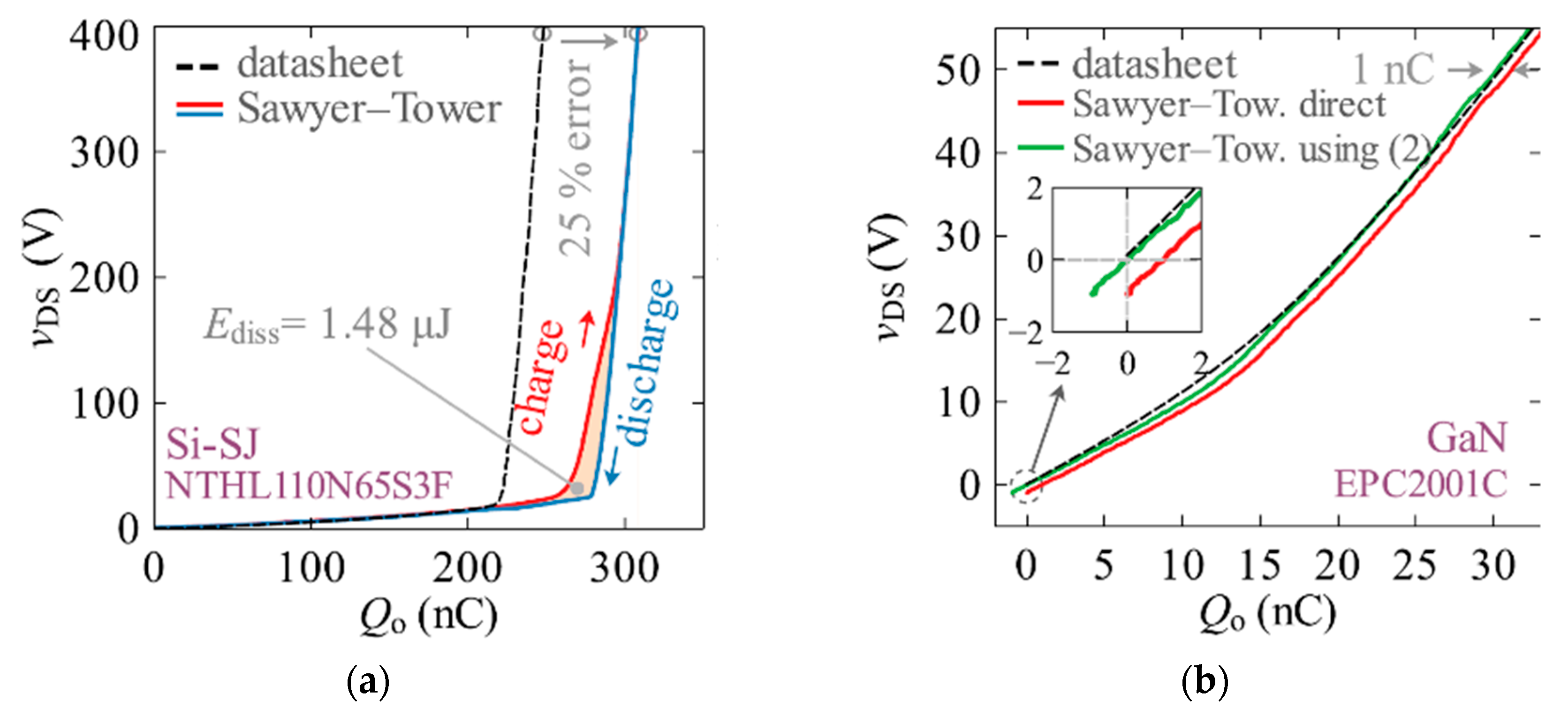
The power device datasheet reports graphs related to the small-signal capacitance. The small-signal capacitance is measured by applying a small perturbation at 1 MHz while the device is off (VGS = 0). This quantity is not useful when there is a difference in the large-signal capacitance because it could lead to an erroneous prediction about the device’s behavior during the commutation. This aspect is important in high-frequency resonant converters, where the use of capacitance datasheet information for circuit simulation could lead to misleading results, especially in terms of switching losses prediction [48]. In Figure 8, a comparison between small-signal (datasheet) and large-signal (measured by means of the Sawyer–Tower circuit) output capacitances is shown [49]. In the GaN HEMT reported in Figure 8, the hysteresis cycle is smaller than the Si counterpart, but, anyway, there is a difference in the output capacitance compared to the datasheet. This phenomenon should be further investigated. An important comparison of output-capacitance hysteresis losses between Si MOSFET, SiC MOSFET, and GaN HEMT is proposed in [50], where a first test has been carried out with constant frequency and voltage. This test has shown that the energy dissipated, Ediss, due to the hysteresis cycle by the SiC MOSFET and GaN HEMT is lower than the Si MOSFET (0.3 µJ vs. 1.5 µJ). On the other hand, the presence of Si MOSFETs in cascode GaN HEMTs implies that they present a more critical Ediss than other GaN HEMTs. Another test has indeed shown that the Ediss increases with increasing applied voltage, especially in the Si MOSFET and, then, in GaN HEMT cascode devices. The tests carried out at variable frequencies have shown that the effect of the frequency on Ediss is negligible.
As explained in Section 4, the circuit models of Si and SiC MOSFETs only account for the small-signal capacitance reported in the datasheet. Therefore, there is not any experience from MOSFETs that can be useful to model the large-signal capacitance and its dependence on the applied voltage in GaN HEMT.

6. Conclusions

When a new MOSFET device is industrialized, it is not necessary to develop a new behavioral model because the adoption of models that already present a good trade-off in terms of accuracy and simulation time is the best approach. In this case, the modeler has to find among them the one providing the optimal trade-off and the values of the parameters of the related mathematical functions. This paper has proved that this approach can also be used for GaN HEMT modeling starting from previous MOSFET models, although the considerations reported in Section 3 and Section 4 have to be taken into account. Therefore, almost no further effort is required for the modeler in modeling new GaN HEMT devices in comparison with new MOSFETs.
On the other hand, this work has also pinpointed the main problems in modeling key static and dynamic quantities of the GaN HEMT. More specifically, the circuit modeling of the dynamic RDS,on and COSS hysteresis has been little investigated in the literature, and, furthermore, there is not any previous MOSFET modeling experience that can be used for GaN HEMT. Neglecting them in circuit models used to simulate GaN-based power converters can lead to inaccurate results involving a non-optimal design that, in turn, lowers efficiency and can involve reliability issues. Therefore, the challenge for researchers involved in GaN modeling is the development of behavioral models of the dynamic RDS,on, large-signal capacitance, and capacitive hysteresis. These models have to be both accurate and computationally low-cost. Another key challenge is the development of models that enable quick computation of the model parameters while simultaneously being endowed with good accuracy and fast simulation.

Author Contributions

Methodology, S.A.R.; Formal analysis, E.A.B. and S.A.R.; Investigation, E.A.B.; Writing—original draft, E.A.B. and S.A.R.; Writing—review & editing, E.A.B. and S.A.R.; Supervision, S.A.R.; Funding acquisition, S.A.R. All authors have read and agreed to the published version of the manuscript.

Funding

This research was partially funded by Ministry of Education, Universities and Research (Italy) under the call PRIN 2017 grant number 2017MS9F49.

Data Availability Statement

The data is reported in the manuscript.

Conflicts of Interest

The authors declare no conflict of interest.

References

  1. Van Do, T.; Trovao, J.P.F.; Li, K.; Boulon, L. Wide-Bandgap Power Semiconductors for Electric Vehicle Systems: Challenges and Trends. IEEE Veh. Technol. Mag. 2021, 16, 89–98. [Google Scholar] [CrossRef]
  2. Luo, D.; Gao, Y.; Mok, P.K.T. A GaN Driver for a Bi-Directional Buck/Boost Converter with Three-Level VGS Protection and Optimal-Point Tracking Dead-Time Control. IEEE Trans. Circuits Syst. I Regul. Pap. 2022, 69, 2212–2224. [Google Scholar] [CrossRef]
  3. Marzoughi, A.; Burgos, R.; Boroyevich, D. Characterization and Performance Evaluation of the State-of-the-Art 3.3 kV 30 A Full-SiC MOSFETs. Trans. Ind. Appl. 2019, 55, 575–583. [Google Scholar] [CrossRef]
  4. Hazra, S.; De, A.; Cheng, L.; Palmour, J.; Schupbach, M.; Hull, B.A.; Allen, S.; Bhattacharya, S. High switching performance of 1700-V, 50-A SiC Power MOSFET over Si IGBT/BiMOSFET for advanced power conversion applications. IEEE Trans. Power Electron. 2016, 31, 4742–4754. [Google Scholar]
  5. Matocha, K.; Dunne, G.; Soloviev, S.; Beaupre, R. Time-Dependent Dielectric Breakdown of 4H-SiC MOS Capacitors and DMOSFETs. IEEE Tran. Electron Dev. 2008, 55, 1830–1834. [Google Scholar] [CrossRef]
  6. Ni, Z.; Lyu, X.; Yadav, O.P.; Singh, B.N.; Zheng, S.; Cao, D. Overview of Real-Time Lifetime Prediction and Extension for SiC Power Converters. IEEE Trans. Power Electron. 2019, 35, 7765–7794. [Google Scholar] [CrossRef]
  7. Lidow, A. GaN as a displacement technology for silicon in power management. In Proceedings of the 2011 IEEE Energy Conversion Congress and Exposition, Phoenix, AZ, USA, 17–22 September 2011; pp. 1–6. [Google Scholar]
  8. Talikoti, N.; Rao, K.U.; Ghosh, R. GAN versus CoolMOS: A theoretical comparison of performances. In Proceedings of the Fifth International Conference on Advances in Recent Technologies in Communication and Computing (ARTCom 2013), Bangalore, India, 20–21 September 2013; pp. 409–414. [Google Scholar]
  9. Musumeci, S.; Mandrile, F.; Barba, V.; Palma, M. Low-Voltage GaN FETs in Motor Control Application; Issues and Advantages: A Review. Energies 2021, 14, 6378. [Google Scholar] [CrossRef]
  10. Kulkarni, A.; Gupta, A.; Mazumder, S.K. Resolving Practical Design Issues in a Single-Phase Grid-Connected GaN-FET-Based Differential-Mode Inverter. IEEE Trans. Power Electron. 2018, 33, 3734–3751. [Google Scholar] [CrossRef]
  11. Khandelwal, S.; Chauhan, Y.S.; Fjeldly, T.A.; Ghosh, S.; Pampori, A.; Mahajan, D.; Dangi, R.; Ahsan, S.A. ASM GaN: Industry Standard Model for GaN RF and Power Devices—Part 1: DC, CV, and RF Model. IEEE Trans. Power Electron. 2019, 66, 80–86. [Google Scholar] [CrossRef]
  12. Cucak, D.; Vasic, M.; Garcia, O.; Oliver, J.A.; Alou, P.; Cobos, J.A.; Wang, A.; Martin-Horcajo, S.; Romero, M.F.; Calle, F. Physics-Based Analytical Model for Input, Output, and Reverse Capacitance of a GaN HEMT With the Field-Plate Structure. IEEE Trans. Power Electron. 2017, 32, 2189–2202. [Google Scholar] [CrossRef]
  13. Albahrani, S.A.; Mahajan, D.; Hodges, J.; Chauhan, Y.S.; Khandelwal, S. ASM GaN: Industry Standard Model for GaN RF and Power Devices—Part-II: Modeling of Charge Trapping. IEEE Trans. Electron Devices 2019, 66, 87–94. [Google Scholar] [CrossRef]
  14. Hontz, M.R.; Chu, R.; Khanna, R. Effect of Substrate Choice on Transient Performance of Lateral GaN FETs. IEEE J. Electron Devices Soc. 2020, 8, 331–335. [Google Scholar] [CrossRef]
  15. Hontz, M.R.; Cao, Y.; Chen, M.; Li, R.; Garrido, A.; Chu, R.; Khanna, R. Modeling and Characterization of Vertical GaN Schottky Diodes With AlGaN Cap Layers. IEEE Trans. Electron Devices 2017, 64, 2172–2178. [Google Scholar] [CrossRef]
  16. Wang, K.; Yang, X.; Li, H.; Ma, H.; Zeng, X.; Chen, W. An Analytical Switching Process Model of Low-Voltage eGaN HEMTs for Loss Calculation. IEEE Trans. Power Electron. 2016, 31, 635–647. [Google Scholar] [CrossRef]
  17. Huang, X.; Li, Q.; Liu, Z.; Lee, F.C. Analytical Loss Model of High Voltage GaN HEMT in Cascode Configuration. IEEE Trans. Power Electron. 2014, 29, 2208–2219. [Google Scholar] [CrossRef]
  18. Wu, X.; Wong, S.C.; Tse, C.K.; Lu, J. Bifurcation behavior of SPICE simulations of switching converters: A systematic analysis of erroneous results. IEEE Trans. Power Electron. 2007, 22, 1743–1752. [Google Scholar] [CrossRef]
  19. The Power MOSFET Application Handbook—Design Engineer’s Guide, NXP Semiconductors, Manchester, United Kingdom. Available online: https://www.nxp.com/docs/en/user-guide/MOSFET-Application-Handbook.pdf (accessed on 7 September 2023).
  20. Mantooth, H.A.; Peng, K.; Santi, E.; Hudgins, J.L. Modeling of Wide Bandgap Power Semiconductor Devices—Part I. IEEE Trans. Electron Devices 2014, 62, 423–433. [Google Scholar] [CrossRef]
  21. Kotecha, R.M.; Hossain, M.; Rashid, A.U.; Emon, A.I.; Zhang, Y.; Mantooth, H.A. Compact Modeling of High-Voltage Gallium Nitride Power Semiconductor Devices for Advanced Power Electronics Design. IEEE Open J. Power Electron. 2021, 2, 75–87. [Google Scholar] [CrossRef]
  22. Wu, L.; Saeedifard, M. A Simple Behavioral Electro-Thermal Model of GaN FETs for SPICE Circuit Simulation. IEEE J. Emerg. Sel. Top. Power Elec. 2016, 4, 730–737. [Google Scholar] [CrossRef]
  23. Bazzano, G.; Raffa, A.; Rizzo, S.A.; Salerno, N.; Susinni, G.; Veneziano, P. Optimization of a SiC MOSFET behavioural circuit model by using a multi-objective genetic algorithm. In Proceedings of the 2020 IEEE Energy Conversion Congress and Exposition (ECCE), Detroit, MI, USA, 11–15 October 2020. [Google Scholar]
  24. Yazgi, M.; Kuntman, H. A new approach for the extraction of SPICE MOSFET Level-3 static model parameters. In Proceedings of the 1998 IEEE International Conference on Electronics, Circuits and Systems. Surfing the Waves of Science and Technology (Cat. No.98EX196), Lisboa, Portugal, 7–10 September 1998. [Google Scholar]
  25. Jadli, U.; Mohd-Yasin, F.; Moghadam, H.A.; Pande, P.; Chaturvedi, M.; Dimitrijev, S. Modeling Power GaN-HEMTs Using Standard MOSFET Equations and Parameters in SPICE. Electronics 2021, 10, 130. [Google Scholar] [CrossRef]
  26. Curtice, W.R.; Ettenberg, M. A Nonlinear GaAs FET Model for Use in the Design of Output Circuits for Power Amplifiers. Trans. Micro. Th. Technol. 1985, 33, 1383–1394. [Google Scholar] [CrossRef]
  27. Endruschat, A.; Novak, C.; Gerstner, H.; Heckel, T.; Joffe, C.; Marz, M. A Universal SPICE Field-Effect Transistor Model Applied on SiC and GaN Transistors. IEEE Trans. Power Electron. 2019, 34, 9131–9145. [Google Scholar] [CrossRef]
  28. Angelov, I.; Zirath, H.; Rosman, N. A new empirical nonlinear model for HEMT and MESFET devices. IEEE Trans. Microw. Theory Tech. 1992, 40, 2258–2266. [Google Scholar] [CrossRef]
  29. Hsu, F.J.; Hung, C.C.; Chu, K.T.; Lee, L.S.; Lee, C.Y. A Dynamic Switching Response Improved SPICE Model for SiC MOSFET with Non-linear Parasitic Capacitance. In Proceedings of the 2020 IEEE Workshop on Wide Bandgap Power Devices and Applications in Asia (WiPDA Asia), Suita, Japan, 23–25 September 2020. [Google Scholar]
  30. Hsu, F.-J.; Yen, C.-T.; Hung, C.-C.; Lee, C.-Y.; Lee, L.-S.; Chu, K.-T.; Li, Y.-F. High accuracy large-signal SPICE model for silicon carbide MOSFET. In Proceedings of the 2018 IEEE 30th International Symposium on Power Semiconductor Devices and ICs (ISPSD), Chicago, IL, USA, 13–17 May 2018; pp. 403–406. [Google Scholar]
  31. Li, K.; Evans, P.L.; Johnson, C.M.; Videt, A.; Idir, N. A GaN-HEMT Compact Model Including Dynamic RDSon Effect for Power Electronics Converters. Energies 2021, 14, 2092. [Google Scholar] [CrossRef]
  32. Peng, K.; Santi, E. Characterization and modeling of a gallium nitride power HEMT. In Proceedings of the 2014 IEEE Energy Conversion Congress and Exposition (ECCE), Pittsburgh, PA, USA, 14–18 September 2014; pp. 113–120. [Google Scholar]
  33. Bottaro, E.; Cacciato, M.; Raffa, A.; Rizzo, S.A.; Salerno, N.; Veneziano, P.P. Development of a SPICE modelling strategy for power devices in GaN technology. In Proceedings of the IECON 2021—47th Annual Conference of the IEEE Industrial Electronics Society, Toronto, ON, Canada, 13–16 October 2021. [Google Scholar]
  34. Li, H.; Zhao, X.; Su, W.; Sun, K.; You, X.; Zheng, T.Q. Nonsegmented PSpice Circuit Model of GaN HEMT with Simulation Convergence Consideration. IEEE Trans. Ind. Electron. 2017, 64, 8992–9000. [Google Scholar] [CrossRef]
  35. Bouchour, A.A.M.; Dherbécourt, P.; Echeverri, A.; El Oualkadi, A.; Latry, O. Modeling of power GaN HEMT for switching circuits applications using Levenberg-Marquardt algorithm. In Proceedings of the 2018 International Symposium on Advanced Electrical and Communication Technologies (ISAECT), Rabat, Morocco, 21–23 November 2018. [Google Scholar]
  36. Wu, C.; Jeng, S. Comparing and modeling power GaN FETs for switching converter applications. In Proceedings of the 2017 International Conference on Applied System Innovation (ICASI), Sapporo, Japan, 13–17 May 2017; pp. 740–743. [Google Scholar]
  37. Okamoto, M.; Toyoda, G.; Hiraki, E.; Tanaka, T.; Hashizume, T.; Kachi, T. Loss evaluation of an AC-AC direct converter with a new GaN HEMT SPICE model. In Proceedings of the 2011 IEEE Energy Conversion Congress and Exposition, Phoenix, AZ, USA, 17–22 September 2011; pp. 1795–1800. [Google Scholar]
  38. Datasheet GaNSystem GS-065-030-2-L. Available online: https://gansystems.com/gan-transistors/gs-065-030-2-l/ (accessed on 8 September 2023).
  39. Yeo, H.L.; Tseng, K.J. Modelling technique utilizing modified sigmoid functions for describing power transistor device capacitances applied on GaN HEMT and silicon MOSFET. In Proceedings of the 2016 IEEE Applied Power Electronics Conference and Exposition (APEC), Long Beach, CA, USA, 20–24 March 2016; pp. 3107–3114. [Google Scholar]
  40. Yang, S.; Han, S.; Sheng, K.; Chen, K.J. Dynamic On-Resistance in GaN Power Devices: Mechanisms, Characterizations, and Modeling. J. Em. Sel. Topics Power El. 2019, 7, 1425–1439. [Google Scholar] [CrossRef]
  41. Li, K.; Evans, P.L.; Johnson, C.M. Characterisation and Modeling of Gallium Nitride Power Semiconductor Devices Dynamic On-State Resistance. Trans. Power El. 2018, 33, 5262–5273. [Google Scholar] [CrossRef]
  42. Zulauf, G.; Guacci, M.; Kolar, J.W. Dynamic on-Resistance in GaN-on-Si HEMTs: Origins, Dependencies, and Future Characterization Frameworks. Tr. Power El. 2020, 35, 5581–5588. [Google Scholar] [CrossRef]
  43. Badawi, N.; Hilt, O.; Bahat-Treidel, E.; Bocker, J.; Wurfl, J.; Dieckerhoff, S. Investigation of the Dynamic On-State Resistance of 600V Normally-Off and Normally-On GaN HEMTs. In Proceedings of the 2015 IEEE Energy Conversion Congress and Exposition (ECCE), Montreal, QC, Canada, 20–24 September 2015. [Google Scholar]
  44. Kohlhepp, B.; Kübrich, D.; Dürbaum, T. Measuring and Modeling of Dynamic On-State Resistance of GaN-HEMTs. In Proceedings of the 2019 21st European Conference on Power Electronics and Applications (EPE ’19 ECCE Europe), Genova, Italy, 3–5 September 2019. [Google Scholar]
  45. Mauromicale, G.; Rizzo, S.A.; Salerno, N.; Susinni, G.; Raciti, A.; Fusillo, F.; Palermo, A.; Scollo, R. Analysis of the impact of the operating parameters on the variation of the dynamic on-state resistance of GaN power devices. In Proceedings of the 2020 2nd IEEE International Conference on Industrial Electronics for Sustainable Energy Systems (IESES), Cagliari, Italy, 1–3 September 2020; pp. 101–106. [Google Scholar]
  46. Li, Y.; Zhao, Y.; Huang, A.Q.; Zhang, L.; Lei, Y.; Yu, R.; Ma, Q.; Huang, Q.; Sen, S.; Jia, Y.; et al. Evaluation and Analysis of Temperature-Dependent Dynamic RDS,on of GaN Power Devices Considering High-Frequency Operation. IEEE J. Emerg. Sel. Top. Power Electron. 2020, 8, 111–123. [Google Scholar] [CrossRef]
  47. Bottaro, E.; Rizzo, S.A.; Salerno, N. Circuit Models of Power MOSFETs Leading the Way of GaN HEMT Modelling—A Review. Energies 2022, 15, 3415. [Google Scholar] [CrossRef]
  48. Tong, Z.; Roig-Guitart, J.; Neyer, T.; Plummer, J.D.; Rivas-Davila, J.M. Origins of Soft-Switching Coss Losses in SiC Power MOSFETs and Diodes for Resonant Converter Applications. IEEE J. Emerg. Sel. Top. Power Electronics 2021, 9, 4082–4095. [Google Scholar] [CrossRef]
  49. Perera, N.; Kampitsis, G.; van Erp, R.; Ancay, J.; Jafari, A.; Nikoo, M.S.; Matioli, E. Analysis of Large-Signal Output Capacitance of Transistors Using Sawyer–Tower Circuit. IEEE J. Emerg. Sel. Top. Power Electron. 2021, 9, 3647–3656. [Google Scholar] [CrossRef]
  50. Perera, N.; Jafari, A.; Nela, L.; Kampitsis, G.; Nikoo, M.S.; Matioli, E. Output-Capacitance Hysteresis Losses of Field-Effect Transistors. In Proceedings of the 2020 IEEE 21st Workshop on Control and Modeling for Power Electronics (COMPEL), Aalborg, Denmark, 9–12 November 2020. [Google Scholar]
Figure 2. Generic circuit model of GaN HEMT.
Energies 16 06574 g002
Figure 3. Use of MOSFET level 3 for GaN modeling: comparison between the OC (A) and TC (B) simulated (red dashed lines) and the measurements (solid green lines) from [25]. The temperature effect is neglected.
Energies 16 06574 g003
Figure 4. Equations accuracy—in terms of average (green) and maximum (red) error (see Equation (2)): OC (A) and TC (B) at 25 °C; OC (C) and TC (D) at higher temperatures; RDS,on (E); TQ (F); CISS (G), COSS (H), and CRSS (I).
Energies 16 06574 g004
Figure 5. Normalized dynamic RDS,on vs. temperature for different operating conditions (credit by [46]). The traces are obtained using measurements.
Energies 16 06574 g005
Figure 6. Implementation of the dependence of the dynamic RDS,on on off-state VDS (a) by using the dependence of the static RDS,on on VGS (b) (credit by [43]). The simulation is the data source.
Energies 16 06574 g006
Figure 7. Dynamic RDS,on: (a) circuit model (b) simulation (credit by [31]).
Energies 16 06574 g007
Figure 8. Comparison between small-signal and large-signal capacitance in (a) Si-SJ MOSFET and (b) GaN HEMT (credit by [49]).
Energies 16 06574 g008
Table 1. Part number of the devices considered in the comparison for each typical characteristic reported in the datasheet and used for setting the parameters of the related behavioral models.
CharacteristicSi MOSFETSiC MOSFETGaN HEMT
OCIPW65R150CFDSCTH35N65G2V-7GS66516T
TCIPB60R360P7IMW65R027M1HGS-065-004-1-L
VTHSTW48N60M2SCTH35N65G2V-7GAN190-650FBE
RDS,onIPB60R360P7SCTH35N65G2V-7GS-065-004-1-L
TQIPB60R360P7IMW65R027M1HGPI65060DFN
COSSSTB30N65M5IMZA65R072M1HGPI65007DF
Disclaimer/Publisher’s Note: The statements, opinions and data contained in all publications are solely those of the individual author(s) and contributor(s) and not of MDPI and/or the editor(s). MDPI and/or the editor(s) disclaim responsibility for any injury to people or property resulting from any ideas, methods, instructions or products referred to in the content.