Article

High-Performance Charge Pump Regulator with Integrated CMOS Voltage Sensing Control Circuit

School of Electrical and Computer Engineering, Chungbuk National University, Cheongju 28644, Republic of Korea
*
Authors to whom correspondence should be addressed.
Energies 2023, 16(12), 4577; https://doi.org/10.3390/en16124577
Submission received: 23 April 2023 / Revised: 2 June 2023 / Accepted: 6 June 2023 / Published: 7 June 2023
(This article belongs to the Special Issue High-Performance Power Converters and Inverters)

Abstract

:
This paper introduces a design for a charge pump DC-DC boost regulator with an integrated low-voltage control circuit. With a charge pump and feedback circuits implemented in 0.35 µm CMOS technology, the proposed DC-DC boost regulator offers an efficient device solution for low-power applications. The proposed design employs an error amplifier, oscillator, and comparator in the control circuit which is designed with a supply voltage of 1.8–3.5 V and 2 MHz frequency. Stability is obtained via a pole-zero compensation in the feedback circuit. The charge pump regulator with four pump stages and the whole regulator circuit are analyzed using the Cadence simulation tool. Measurements of the fabricated 0.35 µm CMOS regulator show that the transient time of the error amplifier is controlled within 1.0 µsec and the output voltage is accurately controlled from 7.8 V to 9.4 V with 27–38 mV ripple and 4.5 mA maximum current.

1. Introduction

In this paper, we present an integrated DC-DC regulator based on the Dickson charge pump. The DC-DC regulator is one of the important components in a power management system because it provides various supply voltages with low power consumption. In particular, battery-operated portable electronic devices require high efficiency and low power consumption DC-DC regulators for long battery operation.
The demand for low-power applications and the proliferation of battery-powered devices have resulted in a steady decrease in the supply voltages of integrated circuits. The power savings that result from a decrease in the supply voltage has been one of the prime motivators for current research efforts which focus on the development of circuit topologies that can operate with lower supply voltage.
Most on-chip DC-DC conversion systems have relied on buck and boost regulators with off-chip LC filters [1]. A capacitor-switched DC-DC boost regulator operates by transferring charges in the booster capacitors to a load capacitor with FET switches. The regulator is usually composed of a switching stage and a feedback control circuit. Among the various elements in the DC-DC regulator [2,3,4], the oscillator and the error amplifier in the control circuit are important for the operation of the overall feedback control which requires a fast-dynamic response [5,6].
Regulators based on the charge pump principles are often used for low-voltage low-current devices operating on battery power [7,8,9]. In this case, the input voltage is supplied by a battery. The regulator makes a constant output voltage with a varying input voltage. A charge pump regulator cannot deliver large currents due to the current limit of integrated-circuit capacitors. The popularity of CMOS devices is entirely due to their ability to design circuits that minimize power consumption.
A charge pump, which requires only capacitors and integrated switches, will thus be used as the primary voltage conversion mechanism. In order for the charge pump to function as a voltage regulator, the circuit must be controlled by a feedback mechanism. The regulation scheme employed in this paper is one that takes advantage of the regulation capabilities of an op-amp. With higher integration density and rapid progress of power management units (PMU), the system on chip (SoC) is being widely employed in low-power applications. As a part of green technology, several voltage levels are required to reduce the power consumption of the chip or system with reliability, stability, and high efficiency. In particular, a step-up voltage regulator is powered by a low-voltage battery and transfers energy to embedded sub-systems that need a high voltage level with extreme stability. There are two types of voltage regulators: linear and switching. The switching regulator is more popular than the linear one because of its higher efficiency as well as small output voltage ripple and wide load current range. Thanks to these advantages, DC-DC converters have recently received a great deal of attention. For the charge pump to function as a voltage regulator, a feedback mechanism is required for a constant output voltage with varying load currents.
A voltage multiplier can be realized with a Dickson charge pump in a way similar to the classic Cockcroft–Walton multiplier. Here, the charge pump functions as a capacitor switched DC-DC booster and regulator. Many topologies of charge pump circuits have been proposed such as series-parallel, bootstrap, static charge transfer switches (CTS), dual-branch, cross-coupled, adiabatic, mixed, and adaptive types [10,11,12].
This paper presents an inductor-less charge pump voltage regulator that employs a pulse width modulation (PWM) technique which suppresses the output voltage ripple, decreases the start-up time, and widens the load current range. The output voltage of the proposed PWM charge pump is regulated by dynamically controlling the duty ratio. The proposed circuit controls the duty ratio automatically with a fast start up and a small output voltage ripple for the regulated output voltage.
The regulation scheme used in this paper takes advantage of the op amp’s regulation capabilities. In the interest of minimizing the cost and size, the DC-DC regulator presented in this paper will not make use of off-chip magnetic elements such as inductors. Instead, off-chip capacitors and resistors will constitute the external elements. The Dickson charge pump is employed for its simplicity and the lack of cumulated voltage drop due to the capacitor’s internal resistance when the load current is high. The regulation of the output voltage is ensured by employing fast-working feedback control-based PWM principles. The contribution of this paper is the combination of the Dickson charge pump with PWM feedback to achieve a high-performance DC-DC regulator. In Section 2, we present a detailed description of the design and operation of the proposed charge pump regulator.

2. Circuit Implementations

2.1. Charge Pump Circuit

Charge pump technology has a long history of development, and several papers have been published on the modeling and analysis of the charge pump [13,14,15].
The Dickson charge pump operates on the push-pull principle where two out-of-phase clocks are used to control successive charges and discharging in each half of the clock cycle [16,17]. The output ripple voltage of a switching-mode regulator can be reduced by using an LC filter. In the charge pump regulator, a large output ripple voltage is generated by pumping capacitors with full power independent of the load resistance. In this work, the output ripple voltage is greatly reduced by using feedback control. Various approaches to enhancing the efficiency of the charge pump have been proposed such as a dynamic biasing of the switching transistor and the use of a current-mode body-biased switch and the so-called deep n-well switching technique [18,19,20].
The proposed regulator is shown in Figure 1. Two building blocks of the proposed charge pump regulator are a switching charge pump stage and a feedback control circuit. The charge pump stage includes two MOS switches and capacitors. The charge pump capacitors CP1 to CP4 shown in Figure 2 are connected externally for design flexibility. The control stage is composed of an error amplifier (error-amp), a comparator, an oscillator, and a gate driver [21,22]. Key elements in the control circuit are the error-amp and the gate driver since they determine the fast feedback performance. The charge pump switch control signals Q1 and Q2 are connected to the charge pump via capacitors CP1 to CP4 as shown in Figure 2. In order to realize an efficient and fully integrated power module, a capacitor-switched DC-DC boost regulator with an on-chip oscillator is designed with a standard 0.35 μm CMOS process. The input voltage to the error-amp is scaled down by R1 and R2. The error-amp, as a compensator, requires a fast-transient response without the slewing problem. High current-driving capability in the current source is also important for the operation of the error-amp.
The charge pumps are widely used in both analog and digital electronic circuits. They perform the voltage conversion by storing the charge on a capacitor and then changing the reference voltage of one of its terminals; the capacitor is referenced to either terminal depending on a step-up conversion or a polarity inversion. The shuttling of the charge into and out of the charge transfer capacitors is achieved efficiently using transistor switches operating at frequencies typically between hundreds of kilohertz and tens of megahertz.
Figure 2 shows the Dickson charge pump employed in this paper where the output voltage that is higher than the supply voltage can be obtained via charge pumping. The Dickson charge pump circuit is often used to generate a voltage higher than the supply voltage.
The charge pump circuit has been studied where capacitors are dynamically charged with one to eight stages by the high-speed switching of transistors. Equation (1) is an expression for the approximate output voltage Vout of the charge pump regulator with n stages [23]. The unit pumping stage of Dickson’s charge pump is made up of a charge transfer gate (CTG) and a coupling capacitor (Cs). In Figure 2, five MOS switches and four capacitors are series-connected to form a CTG. Two clocks are out of phase and have an amplitude equal to the supply voltage.
V o u t = V D D + n C P C P + C S   V c k V t r V t r n I o u t f C P + C S  
The input voltage, stray capacitance, pump capacitance, switching frequency, clock voltage, and output current are denoted by VDD, CS, CP, f, Vck, and Iout, respectively. The voltage associated with the switching-on resistance in the MOSFET is denoted by Vtr. The output-voltage-to-input-voltage ratio is determined by the ratio of the pump and stray capacitances. The output voltage of the Dickson charge pump cannot be a linear function of the number of stages. The charge pump efficiency decreases as the number of stages increases due to the shift in the threshold voltage of the diode-connected MOSFET. With the stray capacitance ignored, Equation (2) defines the ripple voltage where f, Iout, and Cout are the switching frequency, output current, and output capacitance, respectively [24]. The required output voltage with a small ripple can be obtained via feedback control. The output ripple voltage is proportional to the load current, as in Equation (2).
V r i p p l e = I o u t f C o u t  
To avoid problems with the threshold voltage increase, a four-stage charge pump circuit is employed for the boost regulation. To reduce the ripple and obtain an output voltage independent of the load resistance, a four-stage charge pump circuit with feedback control is utilized. The four-stage charge pump circuit has five MOS switches and four capacitors, whose capacitance is 2 pF. Even when the source input or load resistance changes, the output voltage can be constant and stable by employing feedback control. The charge pump DC-DC regulator provides a desired output voltage by switching capacitors to charge or discharge. The output voltage can be boosted from the input voltage to a specified value.

2.2. Error-Amp Circuit

The CMOS operational amplifier used in this paper is shown in Figure 3a. The error-amp circuit is composed of an input differential stage, current mirrors, and a common-source amplifier. The feedback control circuit is realized in a CMOS integrated circuit for chip minimization. It usually includes a compensating passive element to improve the frequency stability. The compensating circuit can be added for stable operation without resonance. The conventional compensator is usually composed of an operational amplifier, capacitors, and resistors to realize poles or zeros in the transfer function. The differential pair in a high conductance is preferred for a fast transient response. In order to improve the phase margin in the frequency response, the differential gain and output resistance are carefully determined with a high current driving capability. In this case, a high-gain differential stage is used for a high-speed operation of the control circuit. A cascode circuit is used for the current source in the differential stage. The differential amplifier is used to obtain high transconductance, and a common-source amplifier is employed in the output buffer. The gain and output resistance of the error-amp is optimized at high drive currents for a sufficient phase margin. The output resistance and differential gain are the important parameters for a stable phase margin in frequency compensation.
Figure 3b is an error-amp with an RC compensation circuit. The inputs of the error-amp are the reference voltage and the divider output. The resistor and capacitor in the feedback circuit are used to generate a pole in the compensator. In terms of the frequency response of the control-to-output transfer function, the Miller theorem can be considered in the analysis of the frequency response. The transfer function of the error-amp is given by Equation (3) where a pole is generated by using the RC circuit.
V c o n t r o l V o u t = A S 1 + s R 3 C 1    
f c = 1 2 π R 3 C 1  
A S = R 3 R 1 + R 2  
In Equations (3)–(5), AS, R3, and C1 are the DC gain, resistance, and capacitance in the compensator. The fc is the compensating frequency determined by the resistance R3 and capacitance C1. Careful analysis is performed in terms of the frequency, stability, and ripple. The phase margin and stability are determined by the transfer function of the error-amp given in Equation (3). The values used for R3 and C1 are 8.8 kΩ and 2.0 pF, respectively. Figure 3c shows the gain of the error-amp versus the frequency, where case (B) with a pole-zero optimization is shown together with that of case (A) without a pole-zero optimization. The effect of the compensator pole frequency on the phase margin and stability is analyzed at 100 kHz–10 MHz. The graph indicates that the phase margins of (A) and (B) are about 22° and 72°, respectively, which means that a higher compensator pole frequency results in a sufficient phase margin and a more stable system. The frequency response of the regulator is determined by the characteristics of the error-amp in the feedback circuit. For an improved phase margin for higher stability, the compensator low-pass filter (LPF) cutoff frequency should be chosen carefully for speed as well as stability.

2.3. Comparator Circuit

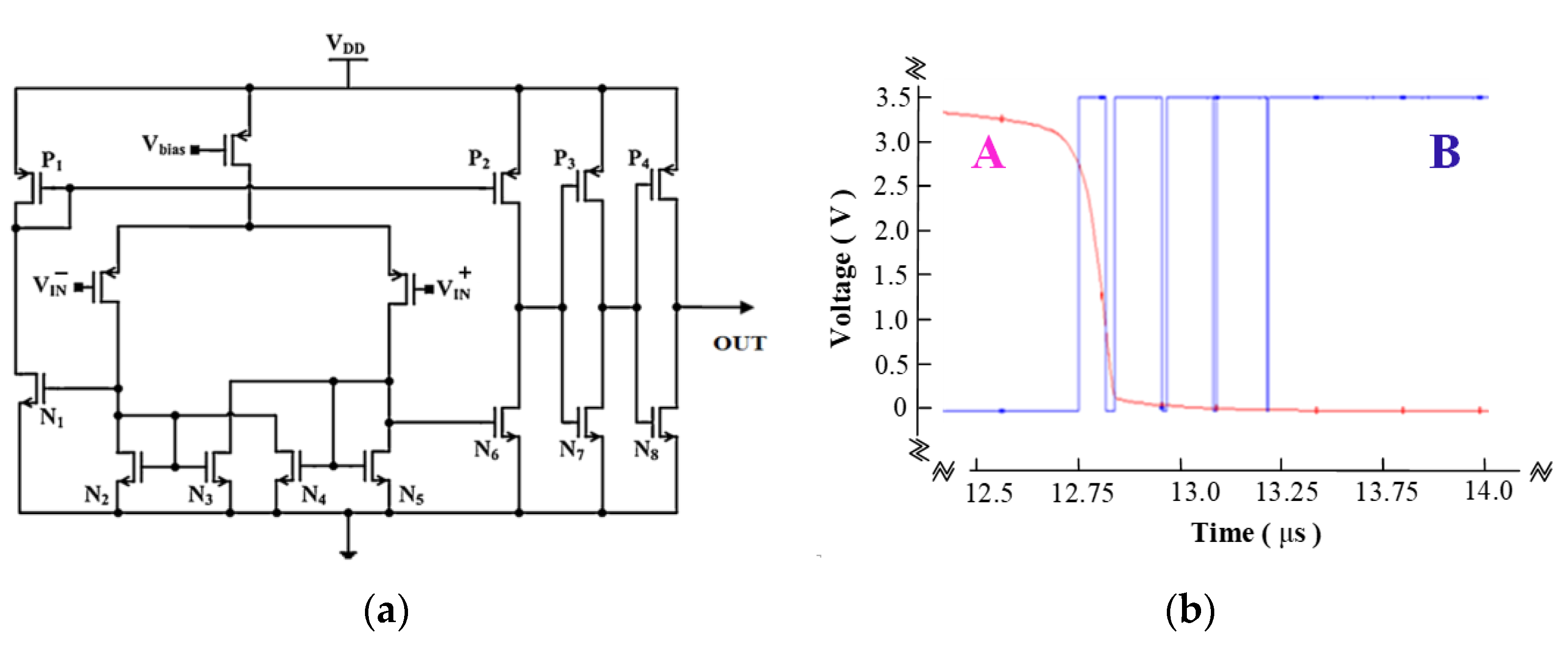
A comparator is used for the pulse-width modulation (PWM) control. The comparator circuit is shown in Figure 4a. It is composed of a bias circuit, an input differential stage, and two output buffers. The input differential stage is an active loaded amplifier. The load circuit consists of inverters connected in a current mirror configuration and thus presents the amplifier with a high resistance load. With modern technologies, a gain of more than 20 is achievable. A clean logic response is obtained by using a latch and an inverter which can function as a gate driver. As a result, the parasitic capacitance is decreased due to reduced-size current-mirror transistors. Figure 4b shows the error-amp output signal (A) and the comparator output signal (B). The output of the error-amp (A) quickly settles down due to the high conductance gm of the differential pair, and the comparator repeats the digital high and low logics until the signal (A) passes a transient response. Waveforms in Figure 4b have been obtained via Cadence simulation.
The output of the error-amp (A) reaches a final value at a high speed owing to the differential pair’s high conductance. After the transient time, the output of the regulator and the duty ratio of PWM is almost constant until a change in load resistance or input voltage. The transient time is about 1.25 µs at 2 MHz with a 3.5 V supply voltage. The proposed feedback control circuit indicates the high-speed operation of the control circuit.
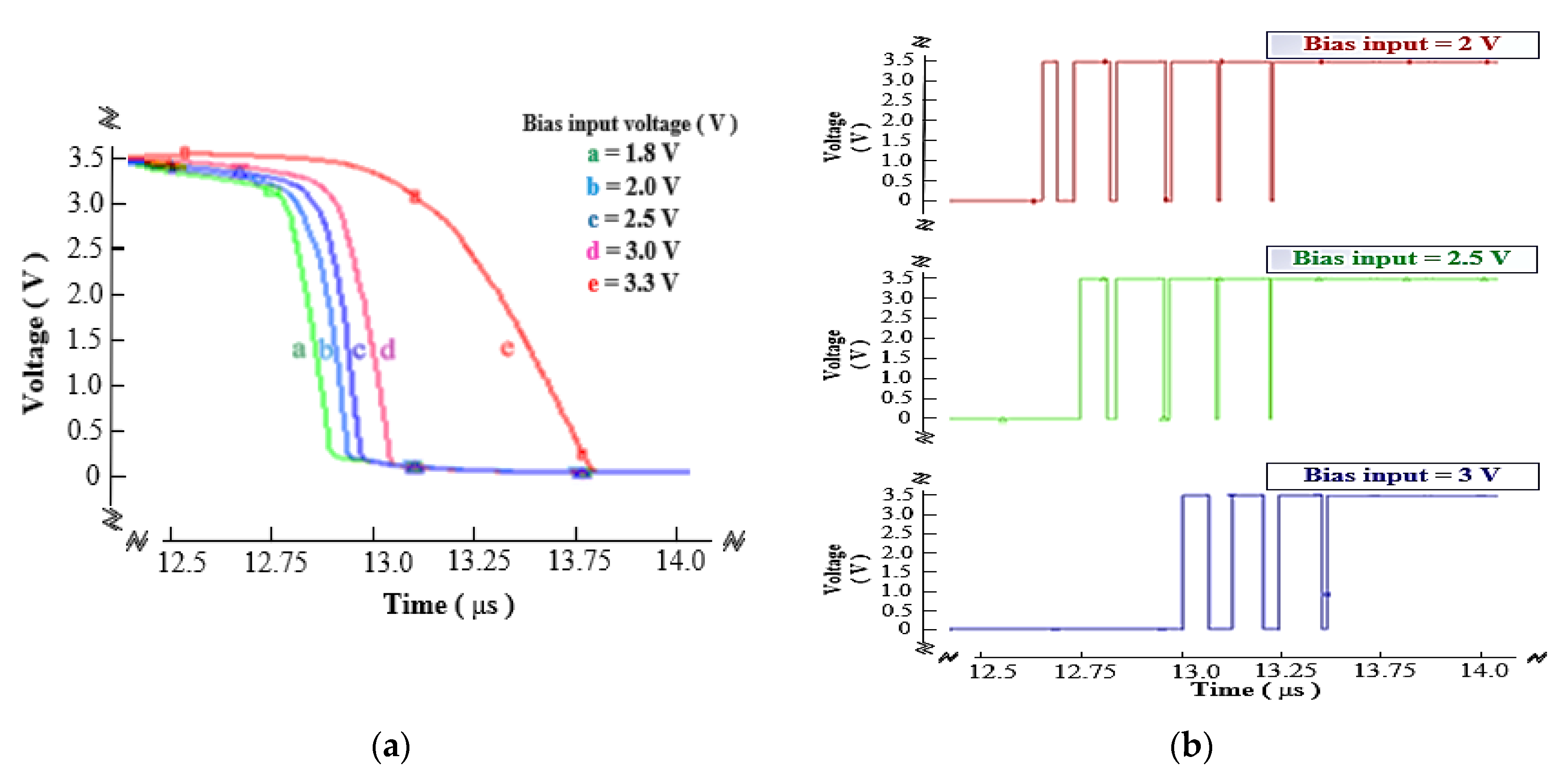
Figure 5 shows the sensitivity of the comparator transient response with respect to the bias input voltage. Figure 5a shows the transient response of the compensator output voltage versus the bias input voltage.
The transient time is smaller with a smaller bias input voltage until 2.5 V. For voltages less than 2.5 V, the transient time shows little change. Figure 5b shows a transient response of the comparator output voltage.

2.4. Oscillator Circuit

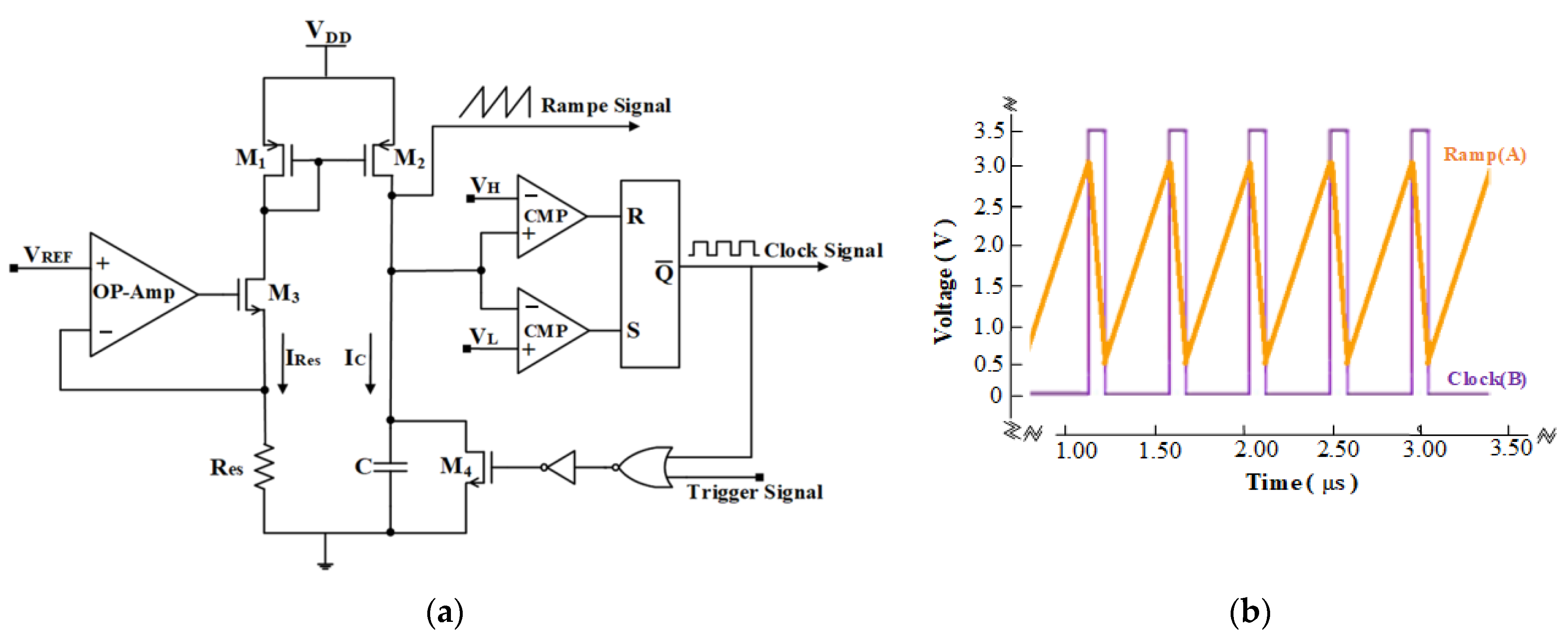
An oscillator is required for the operation of PWM. In PWM switching, the switch control signal is generated by comparing a signal-level control voltage with a repetitive waveform. The oscillator in Figure 6a is implemented with an op-amp and an SR latch to obtain the clock and ramp signals.
The load circuit consists of pMOS transistors connected in a current mirror configuration. A current mirror structure is employed to realize pMOS transistors in the load circuit resulting in a high resistance for the load. The achievable gain with a 0.35 μm CMOS process ranges from 20 to 100. A PWM signal is obtained via a comparison of the comparator voltage with a sawtooth signal. The op-amp output is compared with the oscillator’s sawtooth signal to generate a switch derive signal. A sawtooth signal is generated to make a ramp signal for the comparator. A NOR gate is employed as a feedback element. The clock and ramp signals are shown in Figure 6b. The amplitude, frequency, and duty ratio can be changed by varying the parameters of Res, VH, VL, and VREF. The VH and VL inputs are used to make the peak and valley voltages of the ramp signal. A trigger signal initiates the clock and ramp signals. The signals (A) and (B) in Figure 6b are the clock and ramp signals, respectively. The ramp signal is compared with the reference voltage (VREF) to obtain varying duty ratios. A logic high voltage will be obtained when the sawtooth voltage is less than the error-amp output voltage. The speed of the rising portion of the ramp signal is determined by Res C, while the speed of the falling portion is determined by Ron C, where Ron is the on-state resistance of M4.

2.5. Gate Driver Circuit

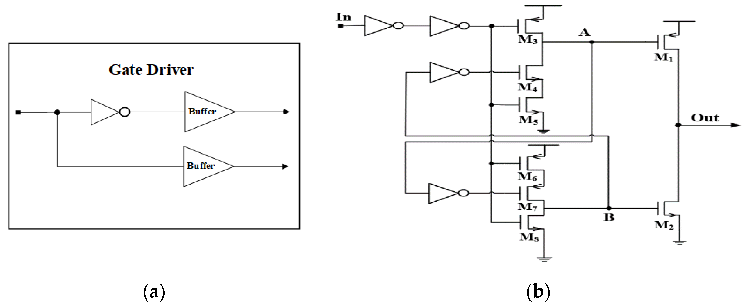
The gate driver circuit with output buffer stages are shown in Figure 7a and Figure 7b, respectively. The buffer circuit should be designed carefully as it can consume a large current during each switching transition and generate a current overshoot. Current overshoot and switching transient are suppressed by making the current flowing in the buffer as small as possible. Power transistors, a feedback loop, and CMOS inverter chains are employed to realize a buffer in Figure 7b. The CMOS inverter chains have different aspect ratios which depend on the channel width and length. A conventional buffer is usually composed of CMOS inverter chains without feedback. It may consume a large amount of power because of the simultaneous turn-on of the up and down transistors in the inverter. Transistors M1 and M2 switch at different times by using the signals (A) and (B) in Figure 7b as the gate drive signal so that the M1 and M2 transistors do not switch simultaneously. No time delay occurs when the transistors are turned on simultaneously. Thus, short circuits can be eliminated by reducing the propagation delay.
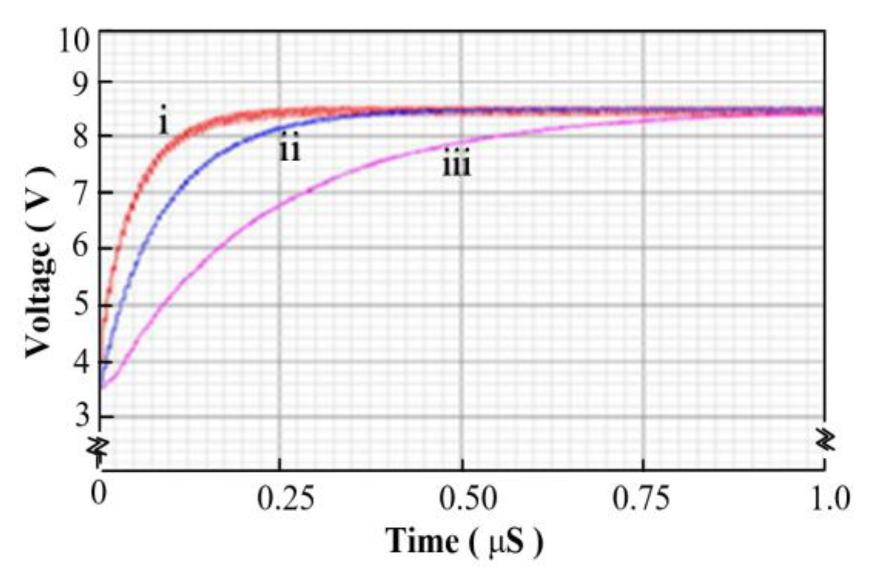
Figure 8 shows the turn-on transient response of the regulator’s output voltage with the switching frequency of 200 kHz (i), 1 MHz (ii), and 2 MHz (iii). The output voltage reaches a steady-state voltage of 8.3 V in a shorter time with a larger switching frequency. The load current is 1.5 mA. The output ripple voltage is smaller with higher switching frequencies: 150 mV with 200 kHz, 60 mV with 1 MHz, and 30 mV with 2 MHz.

3. Results

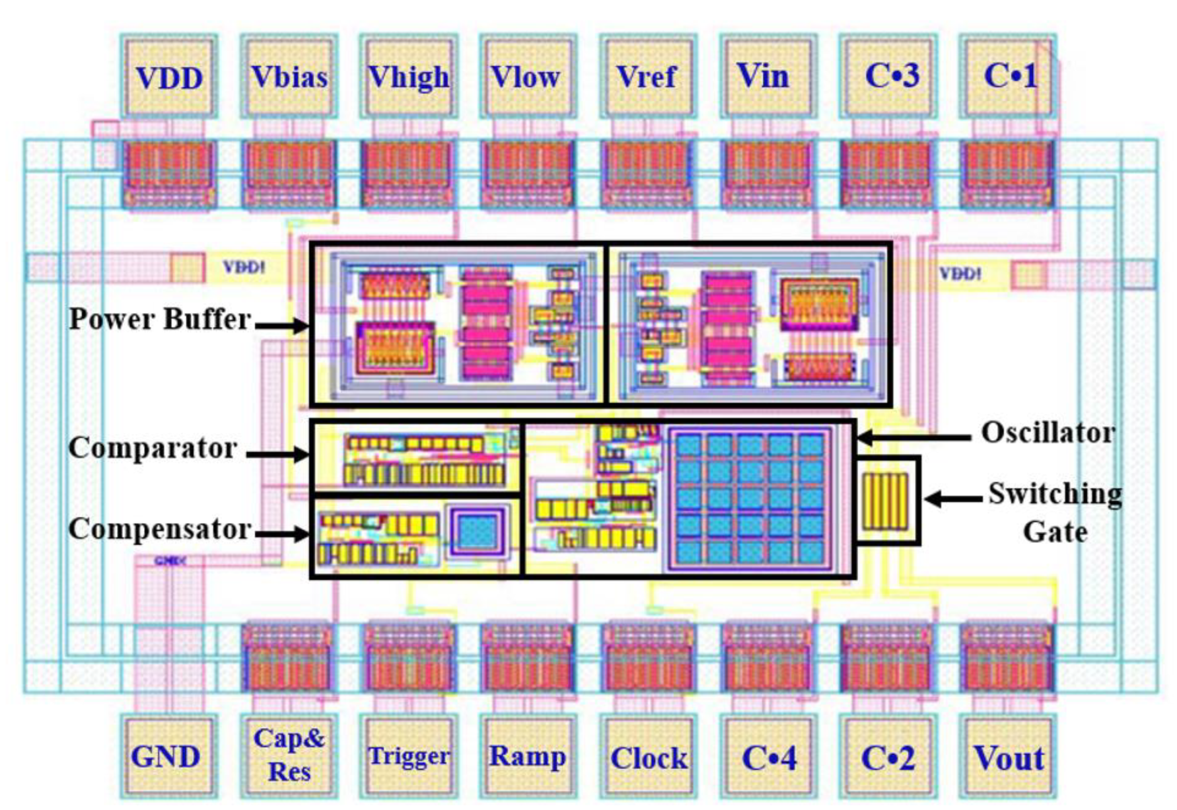
The proposed charge pump DC-DC boost regulator circuit has been designed in 0.35 μm CMOS technology with 2-poly and 4-metal processes. The layout of the proposed charge pump DC-DC boost regulator circuit is shown in Figure 9. The aspect ratios of the device are as follows: 1.0–8.0 in the comparator, 1.5–3.0 in the error-amp, and 1.0–9.0 in the switching gate. Fabrication is performed in a 0.35 μm CMOS process. The circuit has an area of around 1 mm2. Ten prototypes of the fabricated regulator have been tested. Below are the average values of the measurement.
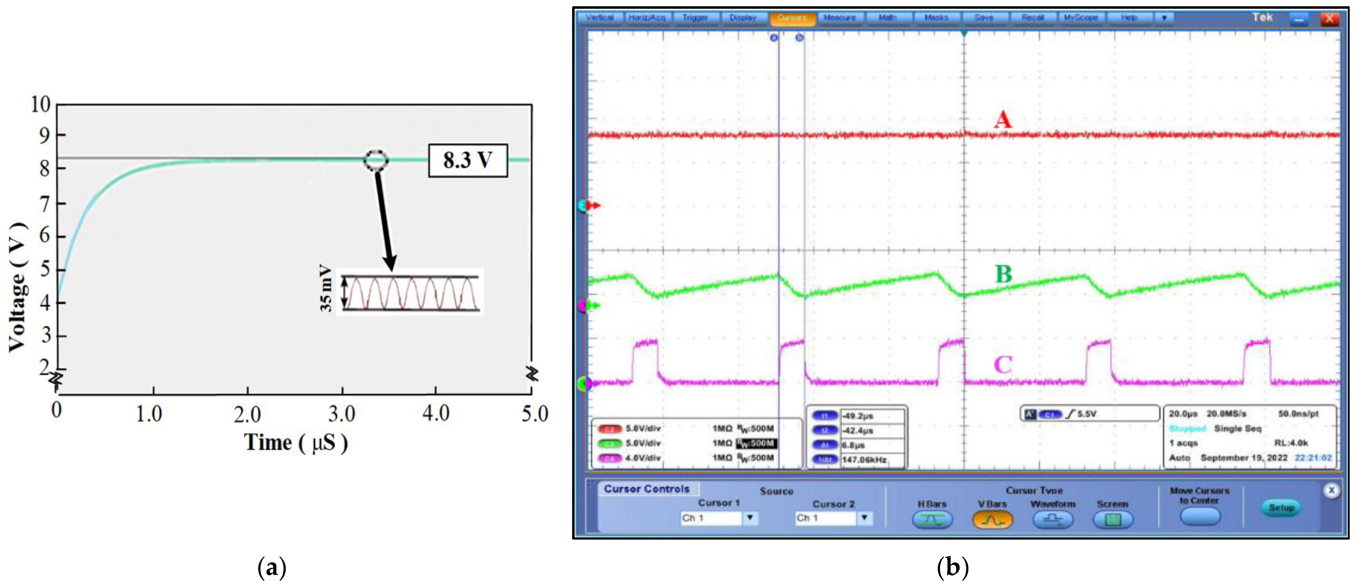
Figure 10a shows that the output voltage of the charge pump regulator is 8.3 V with a 35 mV ripple. In the LC filter regulator, the glitch usually comes from on-off switching transistors in the power block. The advantage of the low output current and ripple can be applied to the LED display driver circuit which usually uses a current of under 10 mA.
However, in this charge pump DC-DC regulator, the glitch is almost negligible. The signals (A), (B), and (C) in Figure 10b are the output voltage, ramp signal, and duty signal, respectively. The PWM signal (C) has a duty of about 20%.
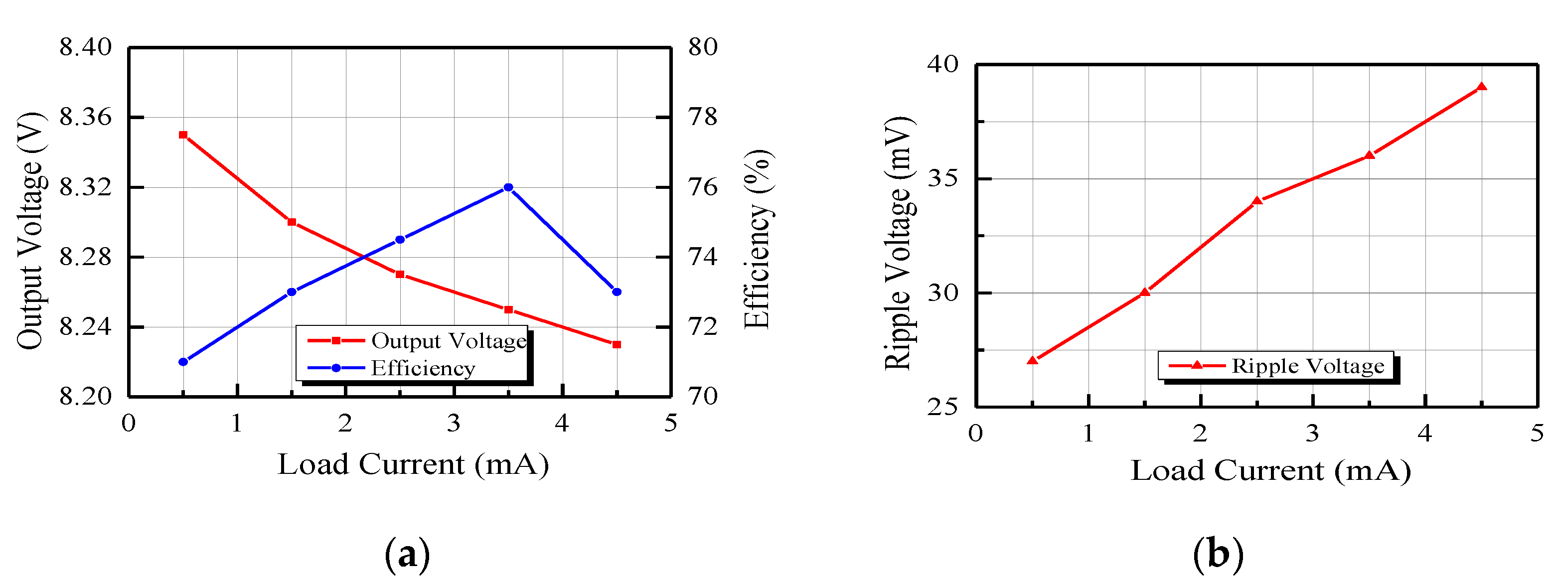
The results imply good uniformity in device performance. Figure 11a shows a test result of the fabricated regulator for 8.3 V output operation. The output voltage change is ±6 mV when the load current varies from 0.5 mA to 4.5 mA. The efficiency maximum is 76% at 3.5 mA load current. Figure 11b shows the peak-to-peak output ripple voltage. The maximum ripple voltage is 38 mV at a load current of 4.5 mA. The output voltage linearly depends on the duty cycle as expected.
The performance of the designed charge pump DC-DC regulator is shown in Table 1. The proposed regulator achieves a high figure of merit with a maximum output current of 4.5 mA and a high power efficiency of 76%. The charge pump regulator without a control circuit shows poor power efficiency.
Table 2 compares the performance of the regulator proposed in this paper with the literature. The performance of the proposed regulator is comparable to other works, validating our design [25,26,27]. The efficiency of the proposed regulator can be increased by using an advanced charge pump configuration and control technique, which is our future research endeavor.

4. Conclusions

An integrated charge pump DC-DC regulator with a voltage control circuit has been proposed in this paper. The Dickson charge pump topology is employed to obtain higher output voltages with lower loss. The output voltage is regulated using a feedback circuit composed of an oscillator, an error-amp, a comparator, and a gate driver. The performance of the proposed regulator has been analyzed using the Cadence MEDICI simulator. The designed regulator has been fabricated using a 0.35 μm CMOS process. The regulator’s performance has been verified with experiments. The regulator uses 1.8–3.5 V input and generates 7.5–8.5 V output with a maximum current of 4.5 mA. From the experimental results, it has been found that the proposed regulator achieves a maximum efficiency of 76% at 8.25 V and 3.5 mA output, which applies to high-performance LED display driver circuits. The charge-pump-based regulator proposed in the paper can be used in low-voltage low-current devices operating on battery power. The limitations of the proposed regulator are a moderate current handling capability for which further study is necessary.

Author Contributions

Conceptualization C.-S.L., I.-S.L. and B.-C.A.; methodology A.M.M., D.B., S.X. and C.-S.L.; validation S.X., D.B., I.-S.L. and C.-S.L.; formal analysis C.-S.L., I.-S.L. and B.-C.A.; formal data curation A.M.M., S.X. and C.-S.L.; writing—original draft, C.-S.L. and B.-C.A.; writing—review and editing, C.-S.L., I.-S.L. and B.-C.A. All authors have read and agreed to the published version of the manuscript.

Funding

This research was supported by the Basic Science Research Program through the National Research Foundation of Korea (NRF) funded by the Ministry of Education, Science and Technology (grant number: NRF-2020R1I1A1A01066637). This research was supported by the MSIT (Ministry of Science and ICT), Korea, under the Grand Information Technology Research Center support program (IITP-2023-2020-0-01462) supervised by the IITP (Institute for Information & communications Technology Planning & Evaluation).

Data Availability Statement

Not applicable.

Acknowledgments

The authors would like to thank IDEC for the CAD tool support.

Conflicts of Interest

The authors declare no conflict of interest.

References

  1. Tao, X.; Xu, J. Integrated current–sensing circuit with offset-current cancellation for boost regulators. In Proceedings of the 2008 International Conference on Communications, Circuits and Systems, Xiamen, China, 25–27 May 2008; pp. 1328–1331. [Google Scholar]
  2. Lee, C.S.; Ko, H.H.; Kim, N.S. Current-mode DC–DC boost regulator with high-performance control circuit. Analog. Integr. Circuits Signal Process. 2014, 80, 105–112. [Google Scholar] [CrossRef]
  3. Lee, C.S.; Gendensuren, M.; Bayarsaikhan, D.; Ahn, B.C.; Choi, S.G. Integrated 0.35-µm CMOS Control Circuits for High Performance Voltage-Mode DC-DC Boost Regulator. Electronics 2022, 12, 133. [Google Scholar] [CrossRef]
  4. Park, J.W.; Gendensuren, M.; Lee, C.S.; Lee, H.G.; Kim, N.S. Charge Pump Regulation with Integrated 0.35 µm CMOS Control Circuit. In Proceedings of the 2012 International Symposium on Signals, Systems, and Electronics (ISSSE), Potsdam, Germany, 3–5 October 2012; pp. 391–394. [Google Scholar]
  5. Chae, C.S.; Le, H.P.; Lee, K.C.; Cho, G.H. A single- inductor step-up DC-DC switching regulator with bipolar outputs for active matrix OLED mobile display panels. IEEE J. Solid-State Circuits 2009, 44, 509–524. [Google Scholar] [CrossRef]
  6. Rahman, L.F.; Marufuzzaman, M.; Alam, L.; Mokhtar, M.B. Design topologies of a CMOS charge pump circuit for low power applications. Electronics 2021, 10, 676. [Google Scholar] [CrossRef]
  7. Ma, X.; Wang, L.; Yu, J. A 5 V-to-32 V input PVT-robust charge-pump circuit with adjustable output in a 0.18 μm BCD process. Electronics 2022, 11, 2828. [Google Scholar] [CrossRef]
  8. Navidi, M.M.; Graham, D.W. A regulated charge pump with extremely low output ripple. Electronics 2022, 8, 1293. [Google Scholar] [CrossRef] [Green Version]
  9. Ballo, A.; Grasso, A.D.; Palumbo, G. A review of charge pump topologies for the power management of IoT nodes. Electronics 2019, 8, 480. [Google Scholar] [CrossRef] [Green Version]
  10. Lim, M.I.; Mi, S.; Sampe, J.; Ali, S.H.M. Review of Charge Pump Topologies for Micro Energy Harvesting Systems. Am. J. Appl. Sci. 2016, 13, 628–645. [Google Scholar]
  11. Mahmoud, A.; Alhawari, M.; Mohammad, B.; Saleh, H.; Ismail, M. A gain-controlled low-leakage Dickson charge pump for energy-harvesting applications. IEEE Trans. J. 2019, 27, 1114–1123. [Google Scholar] [CrossRef]
  12. Kuo, P.H.; Wong, O.-Y.; Tzeng, C.K.; Wu, P.W.; Chiao, C.C.; Chen, P.H.; Chen, P.C.; Tsai, Y.C.; Chu, F.L.; Ohta, J.; et al. Improved charge pump design and ex vivo experimental validation of CMOS 256-pixel photovoltaic-powered subretinal prosthetic chip. IEEE Trans. J. Biomed. Eng. 2020, 67, 1490–1504. [Google Scholar] [CrossRef]
  13. Toru, T. An Analytical Model of Charge Pump DC-DC Voltage Multiplier Using Diodes. IEICE Trans. Fundam. Electron. Commun. Comput. Sci. 2017, E100, 1137–1144. [Google Scholar]
  14. Ballo, A.; Grasso, A.D.; Palumbo, G.; Tanzawa, T. A Charge Loss Aware Advanced Model of Dickson Voltage Multipliers. IEEE Access J. Vol. 2022, 10, 118082–118092. [Google Scholar] [CrossRef]
  15. Aloqlah, A.S.; Alhawari, M. A resistor-network model of Dickson charge pump using steady-state analysis. Energ. J. Mar. 2022, 15, 1899. [Google Scholar] [CrossRef]
  16. Du, H.; Lai, X.; Liu, C.; Chi, Y. Low quiescent current linear regulator using combination structure of bandgap and error amplifier. Electron. Lett. 2014, 50, 771–773. [Google Scholar] [CrossRef]
  17. Liu, P.; Chen, T.; Hsu, S. Area-efficient error amplifier with current-boosting module for fast-transient buck regulators. IET Power Electron. 2016, 9, 2147–2153. [Google Scholar] [CrossRef]
  18. Feng, P.; Li, Y.; Wu, N. A high efficiency charge pump circuit for low power applications. J. Semicond. 2010, 31, 015009. [Google Scholar]
  19. Ballo, A.; Grasso, A.D.; Palumbo, G. Current-mode body-biased switch to increase performance of linear charge pumps. Int. J. Circuit Theory Appl. 2020, 48, 1864–1872. [Google Scholar] [CrossRef]
  20. Lilic, N.; Kappel, R.; Roehrer, G.; Zimmermann, H. Methods for the Charge Pump Power Efficiency Improvement in Triple Well Technologies. In Proceedings of the 2020 27th IEEE International Conference on Electronics, Circuits and Systems (ICECS), Glasgow, UK, 23–25 November 2020; pp. 1–4. [Google Scholar]
  21. Tanzawa, T.; Tanaka, T. A dynamic analysis of the Dickson charge pump. IEEE J. Solid-State Circuits 1997, 32, 1231–1240. [Google Scholar] [CrossRef]
  22. Roh, J. High-performance error amplifier for fast transient DC-DC regulators. IEEE Trans. Circuits Syst. II Express Briefs 2005, 52, 591–595. [Google Scholar]
  23. Dickson, F.F. On-chip high-voltage generation in nMOS integrated circuits using an improved voltage multiplier technique. IEEE J. Solid-State Circuits 1976, SC-1142, 374–378. [Google Scholar] [CrossRef]
  24. Yoo, C.S.; Lee, K.L. A low ripple poly-Si TFT charge pump for driver-integrated LCD pane. IEEE Trans. Consum. Electron. 2005, 51, 606–610. [Google Scholar]
  25. Dong-Sheng, L.; Xue-Cheng, Z.; Fan, Z.; Min, D. Embeded EEPROM memory achieving lower power-new design of EEPROM memory for RFID tag IC. IEEE Circuits Devices Mag. 2006, 22, 53–59. [Google Scholar] [CrossRef]
  26. Rumberg, B.; Graham, D.W.; Navidi, M.M. A regulated charge pump for tunneling floating-gate transistors. IEEE Trans. Circuit Syst. Express Briefs 2017, 64, 516–527. [Google Scholar]
  27. Rahman, L.F.; Alam, L.; Marufuzzaman, M. Design of a Low Power and High-Efficiency Charge Pump Circuit for RFID Transponder EEPROM. Inf. MIDEM 2021, 50, 255–262. [Google Scholar]
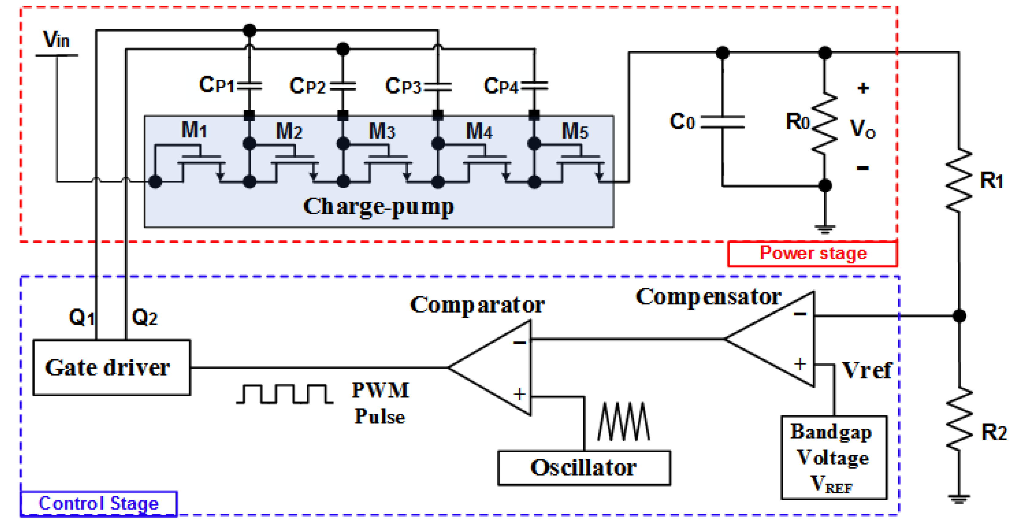
Figure 1. Block diagram of the proposed regulator.
Energies 16 04577 g001
Figure 2. Schematic of voltage regulation by charge pumping.
Energies 16 04577 g002
Figure 3. Error-amp circuit: (a) circuit diagram; (b) compensator circuit; (c) frequency response of the loop gain (A: without pole-zero optimization; B: with pole-zero optimization).
Energies 16 04577 g003
Figure 4. Proposed comparator circuit: (a) comparator circuit; (b) outputs of the error-amp (A) and comparator (B).
Energies 16 04577 g004
Figure 5. Sensitivity of the comparator transient response with respect to bias input voltage: (a) compensator output voltage; (b) comparator output voltage.
Energies 16 04577 g005
Figure 6. Proposed oscillator: (a) oscillator circuit; (b) clock signal (A) and ramp signal (B).
Energies 16 04577 g006
Figure 7. (a) Gate driver circuit; (b) power buffer circuit.
Energies 16 04577 g007
Figure 8. Output voltage turn-on transient versus the switching frequency.
Energies 16 04577 g008
Figure 9. The layout of the charge pump regulator.
Energies 16 04577 g009
Figure 10. Simulation and experimental results: (a) simulated output and ripple voltages; (b) measured output voltage (A), ramp signal (B), and PWM signal (C).
Energies 16 04577 g010
Figure 11. (a) Measure output voltage and efficiency vs. load current; (b) voltage ripple.
Energies 16 04577 g011
Table 1. Performance summary.
ParametersProposed Charge PumpOnly Charge Pump
Load Resistor (R0)20 kΩ20 kΩ
Load Capacitor (C0)47 nF47 nF
Input Voltage (VIN)1.8–3.5 V1.8–3.5 V
Output Voltage (Vout)7.5–9.5 V7.5–9.5 V (Unregulated)
Load Current (IL)4.5 mA (max)4.5 mA (max)
Switching Frequency (fs)2 MHz2 MHz
Ripple Voltage (Vripple)27–38 mV52–95 mV
Efficiency (Sim)76% (max)50% (max)
Table 2. Performance comparison of the proposed regulator.
Sample No.This Work[25][26][27]
Regulator typeCharge pumpDynamic CTSRegulated CPEnhanced-NCP2CTS
Process (μm)0.350.350.350.18
Input Voltage (V)1.8–3.53.32.51.8
Output Voltage (V)7.5–9.52.5–5165.95
Die Area (mm2)1.00.6692.4
Switching Frequency (MHz)233020
Efficiency (%)76 (Sim)-3466
Disclaimer/Publisher’s Note: The statements, opinions and data contained in all publications are solely those of the individual author(s) and contributor(s) and not of MDPI and/or the editor(s). MDPI and/or the editor(s) disclaim responsibility for any injury to people or property resulting from any ideas, methods, instructions or products referred to in the content.