1. Introduction
From its introduction to the present day, researchers have paid special attention to the development of multilevel converters, with the aim of allowing the industry to take advantage of the great number of features offered by multilevel topologies [
1,
2,
3]. One of the most common multilevel converter topologies is the cascaded H-bridge converter (CHB), shown in
Figure 1. Cascaded H-bridge converters play a relevant role in applications such as the integration of renewable energy [
4,
5,
6,
7], Synchronous Compensator (STATCOM) [
8,
9,
10,
11], power distribution applications [
12,
13] and railway traction systems [
14,
15].
Moreover, the CHB topology combines some interesting properties, such as modularity or independent DC sources. The latter allows the use of this topology in a new range of new possibilities in the industry, such as the integration of energy storage systems (ESS) [
16]. This issue is also interesting in photovoltaic plants, where different maximum power points for each array can be tracked independently [
17,
18]. Depending on the application, the control of these converters focuses either on ensuring the voltage balance of the modules or on treating each module differently [
19].
Emerging trends in CHB studies focus on exploiting redundancies in the topology to ensure the voltage balance in the converter. First, a solution to the DC-link voltage balance problem is given in [
20] within the modulation stage. In this work, the carrier is modified, depending on the voltage of the modules, to ensure voltage balancing. A similar approach was taken in [
21], where the carrier waveform was modified with the same objective. Secondly, control techniques [
22,
23,
24] are revised to add triple voltage harmonics or the zero-sequence with the aim of achieving balance. Finally, in some optimal control methods, such as [
11,
25], the objective functions were modified in order to include the balancing problem, benefitting from the redundancies.
New researches are specialized in improving topology efficiency in both balanced and unbalanced situations [
26,
27]. In this sense, [
28] explores the necessity of efficient and reliable power systems and how to improve the lifetime and performance of converters. This research considers the thermal conditions and attempts to reduce the degradation caused by over-switching without interfering with the performance. This problem takes special relevance in hybrid applications such as [
29]. In these situations, a lower number of commutations can improve the lifetime of the ESS and reduce the switching losses of the modules, resulting in great economic savings. In [
30,
31,
32], the modification of the modulation strategy is intended to reduce the switching losses. In [
30], this strategy takes advantage of redundancies in topologies to swap module references, minimizing switching losses. However, great distortion can be produced by eliminating these commutations. In [
31,
32], hybrid modulation techniques were proposed to minimize switching losses while achieving good grid current quality and balancing these losses between modules. Thus, thermal and balancing conditions were considered. Subsequently, [
33] went one step further by applying the half-height (HH) technique. This strategy achieves good current quality and low THD in spite of using a low switching frequency. Therefore, switching losses are maintained at an acceptable level.
The importance of reducing losses in power converters is evident. When designing new control methods, the effective switching frequency must be considered. In this regard, the present paper proposes an improvement over the method disclosed in [
34] to reduce switching losses. In particular, it modifies the objective function of the method to penalize unnecessary commutations between control cycles. Additionally, the severity of commutation losses was considered, avoiding those that occur when the current is high and favoring commutations that occur when the current is low. As a result, this proposal combines DC-link voltage balance, DC voltage and ripple limitation on some selected modules, and switching losses reduction on the other modules. These three objectives and their relative importance can be configured independently for each module.
The rest of this paper is structured as follows.
Section 2 describes the mathematical fundaments of the proposed improvement. It discusses how the objective function is modified and how the different objectives interact with each other.
Section 3 describes the materials and methods used to test the upgraded method. The tests include a comparison with the original method from [
34] with different configurations.
Section 4 describes these tests and shows their results.
Section 5 discusses these results and their implications. Finally, the paper is concluded in
Section 6.
2. Fundaments and Strategy
The proposed method is based on a previously disclosed method [
34] with the aim to improve it. The original method from [
34] was designed for a CHB with three phases and modules per phase. It selects all modules’ output voltages so that they meet a required phase-to-phase voltage while aiming to maximize a certain objective function. As a result, the method solves a linear optimization problem (LOP) in each control cycle.
The LOP constraints are related to the desired phase-to-phase voltages and to the possible outputs of the modules. The objective function is related to the modules’ DC-link voltages and power. This objective function is described in terms of benefit values, which represent the improvement of increasing each module output by 1 V.
The upgrade proposed in this paper is related to the aforementioned objective function. In particular, it is proposed to consider the benefit of avoiding some unnecessary commutations. This way, the effective switching frequency of the transistors is lower, and they produce less heat, which extends their lifespan. No changes need to be made to the LOP constraints or general structure. Thus, the original algorithm can still be employed to solve the new LOP.
2.1. Variables and Constraints
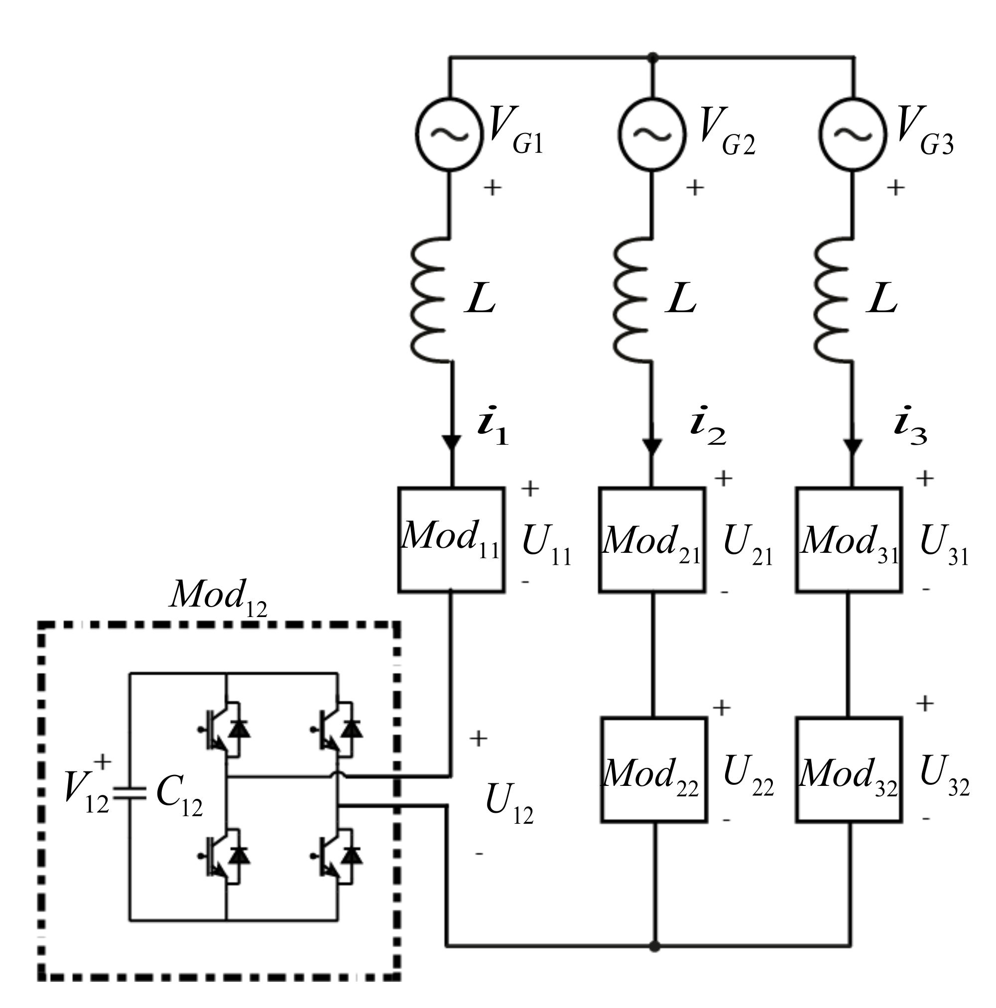
As shown in
Figure 1, a CHB comprises several modules in each phase. Each of these modules can produce any output voltage (
,
,
…
) within a certain range by means of PWM. By selecting different output voltages combinations, the converter currents (
,
and
) and the DC-link voltages (
,
,
…
) can be manipulated in one way or another. Therefore, control methods for CHBs select these modules output voltages
according to some goals.
The most common strategies divide the control problem into two stages. Firstly, a current regulation layer selects the total voltage (, and ) that must be modulated by each phase in order to control the currents. Secondly, a modulation control layer selects one combination of output voltages that matches the desired total phase voltages (, and ). The combination is selected according to a certain DC-link-related objective, which typically includes balancing the modules’ DC-link voltages.
The method proposed in this paper is meant to be applied only in the modulation layer. It is assumed that a current regulation layer has previously calculated the desired total phase voltages (, and ). According to the proposed method, the combination of modules output voltages is selected to maximize a certain objective function in a linear optimization problem. Thus, the LOP variables are the modules output voltages: , , , , , etc.
These voltages must be selected according to the total phase voltages indicated by the current regulation layer. Consequently, there are some current-regulation-related constraints. The simplest way to apply these constraints is to force the desired voltage phase by phase.
Although valid, this set of constraints ignores an important redundancy of the converter: the common-mode voltage. Since the neutral point of the converter is not connected to the grid or any other circuit, any common-mode voltage may be added to all phases without having any impact on currents. Only phase-to-phase voltage needs to be observed instead of phase-to-neutral voltage. Therefore, the set of constraints given by (2) is more accurate.
In addition, due to the H-bridge topology, any module output voltage is limited by its corresponding DC-link voltage. Thus, for example, must remain between and .
2.2. Transition Commutations
After introducing the variables and constraints, only the objective function must be defined to determine the LOP fully. The objective function evaluates how much a LOP solution helps in achieving certain goals. Some of these goals were introduced in [
34]. In this paper, one more objective is considered: the reduction of the switching losses. This goal was intended to be reached by avoiding some commutations that typically occur in the transition from one control cycle to the next.
The origin of these transition commutations was illustrated using an example in which the CHB comprises only two modules per phase, as in
Figure 1. For simplicity, in this example, all DC-links were considered to stay charged at 200 V, as if they were connected to external voltage sources.
At a certain control cycle, the desired phase output voltages are 282 V for the first phase, 0 V for the second phase and −282 V for the third phase. Since only phase-to-phase voltages need to be observed, these voltages represent two constraints.
This linear equation system has six variables but only two linearly independent equations, so four variables may be selected arbitrarily. In LOPs, arbitrarily selected variables are known to always become saturated, either to their maximum or minimum possible values. The other two variables are chosen to meet their respective equations.
The selection of these saturated and nonsaturated variables depends on the objective function. A possible solution is as follows.
According to this solution, during the next control period, two modules need to produce 82 V and −82 V by means of PWM, while the remaining modules remain in a fixed state.
In the next control cycle, the desired phase voltages are 306 V, −57 V and −249 V, respectively. As stated previously, only the phase-to-phase voltage needs to be observed, so any common-mode voltage may be added to the three desired phase voltages. Consider the following two possible solutions (none of them necessarily being optimal):
In both cases, the common-mode voltage added to the three phases is 57 V, but the final combinations of the output voltages are different. If the solution given by (5) is selected, then the four modules that were previously saturated will remain saturated. No additional commutations occur other than those due to PWM. If the solution given by (6) is selected, then both modules in phase 2 have to switch from a saturated state to the other, which produces extra commutations. Furthermore, depending on the type of modulation signals, additional commutations may occur in the modules in phase 1.
These transition commutations that occur when switching between LOP solutions accumulate over the control cycles, producing losses. The proposed strategy to reduce switching losses is to consider the previous state of each module: high-saturated, low-saturated, or nonsaturated. In general, a transition where several modules are maintained on the same state (such as the transition from (4) to (5)) is more beneficial than a transition where several modules change state (such as the transition from (4) to (6)). In order to correctly define the corresponding objective function, this benefit needs to be quantified.
2.3. Objective Function for Switching Losses Reduction
Let
be the current in phase
with the sign shown in
Figure 1 (
). Let
and
be the DC-link voltage and the output voltage of module
in phase
(
). The module duty cycle
can be defined as the proportion between
and
.
The module’s previous state can be defined as 1 for modules that were high-saturated on the previous control cycle, −1 for modules that were low-saturated, and 0 for the other modules. In general, it is beneficial for saturated modules to maintain their state to prevent transition commutations. Thus, if , then there is some benefit in having . For nonsaturated modules (), the states of the transistors at the end of the control cycle are unknown, so there is no guarantee that there would be any benefit in setting to any particular value.
However, not all transition commutations are equally harmful. The losses produced by the commutation of a module are proportional to the product of the module DC-link voltage and the phase current. The greater these potential losses, the more important it is to prevent the commutation. Thus, it is important to avoid transition commutations when the phase current is high, but it is acceptable to have them when the phase current is close to zero (zero-current switching). A partial objective function
for switching reduction can be defined, as in (8).
is a dimensionless gain representing how important it is to reduce the switching in module of phase . This importance is relative to the other objectives of the global objective function. is the absolute value of the corresponding phase current. The greater , and are, the more important it is for to be equal to . Thus, maximizing prevents as many transition commutations losses as possible.
Substituting (7) into (8) and grouping known values produces the same structure used in [
34] for the other partial objective functions.
represents the marginal benefit of increasing by one volt regarding the aforementioned goal. Thus, if was intended to be maximized alone, then modules with high would become high-saturated, whereas modules with low would become low-saturated.
2.4. Integration and Interaction with Other Objectives
In addition, to avoid unnecessary commutations, the modulation layer has other objectives. Two other objectives were already defined in [
34] with the corresponding partial objective functions:
for voltage balancing, and
for ripple reduction. Since the LOP defined in [
34] has a structure similar to the one presented here, these partial objective functions can be combined with
for better results.
2.4.1. Combination with DC-Link Voltage Objective
The most important objective proposed in [
34] is the independent DC-link voltage control. The corresponding partial objective function is
.
is a dimensionless gain, similar to , which represents how important it is for the corresponding module to reach the desired DC-link voltage . As with , this importance is relative to other modules and other objectives.
In order to combine both objectives, the respective objective functions were added together. The resulting LOP is given by (13).
When combining two or more different objectives, they may interfere with each other depending on the situation. Since the optimization problem is linear, each module behavior will correspond to the most beneficial objective in each control cycle, sometimes ignoring the others. Thus, it is important to consider how the new switching reduction objective interacts with the voltage control objective. Therefore, the partial benefit of the voltage control goal, given by (12), can be compared with the combined benefit given by (14).
When comparing (14) to (12), the desired voltage is found to deviate from its original value
. The deviation will sometimes be positive and sometimes negative depending on the signs of the phase current (
) and module previous state (
). This indicates that the deviation will occur in the form of voltage ripple. Since
and the sign function is always between −1 and +1, the maximum deviation of
is
Considering that
, though oscillating, will be close to
, the relative deviation of
can be estimated as in (16).
From this estimation, it can be said that the addition of the transition commutations reduction increase the ripple of the corresponding DC-link voltage . The added ripple is given by the relationship between and . This provides a limit for the gain depending on the acceptable ripple.
2.4.2. Combination with DC-Link Ripple Reduction
Another objective considered in [
34] was the reduction of the DC ripple and the control of the DC power (for modules with ultracapacitors or other energy storage systems). According to [
34], the formulation of the corresponding partial objective function requires parameterizing
, as in (17).
For modules without any energy storage systems, where modules only need to exchange reactive power,
is always null.
is non-negative, and
is nonpositive. In addition, the benefit of increasing
is always lower or equal to the benefit of increasing
. In this way, the objective function considers a certain benefit in
being close to
. When
is 0, the instantaneous power received by the module is closer to 0, thus limiting the DC-ripple. The partial objective function
is as follows.
is a dimensionless gain similar to
and
, and
and
are the partial benefits corresponding to
and
. Please refer to [
34] for more details.
In order to combine the three objectives, the respective objective functions are added together in a global objective function
, which is intended to be maximized. Gains
,
and
can be adjusted independently for each module to prioritize one or another objective according to the application.
The behavior of each module now depends on two global benefit values ( and ) instead of just one. Their effect is now illustrated using these three cases.
If both and are high (relative to other benefit values), then there is a significant benefit in having a high value of . In the optimal solution, the module would probably be high-saturated;
If both and are low (i.e., if they have a big negative value), then there is a significant benefit in having a low value of . In the optimal solution, the module would probably be low-saturated;
If is significantly lower than (the opposite cannot occur), then there is a significant benefit in setting to a particular voltage , which depends on the module’s desired active power. The module would probably modulate this voltage through PWM. This third case only occurs when the power control and ripple reduction objective is selected for the corresponding module (); otherwise, .
The complete LOP is shown in (24). For simplification,
was considered to be null for all modules.
The experimental results from [
34] showed that including the ripple reduction objective (by selecting
) produced a very high number of commutations in the corresponding modules. Equations (14)–(16) of the present paper show that the inclusion of the switching reduction objective (by selecting
) produce the opposite effect: the number of commutations will decrease at the cost of increasing the ripple. Thus, these two objectives oppose each other.
For this reason, these objectives are incompatible with each other in any particular module. Consequently, for each module, it is advised that at least one of these gains (
or
) is made null. Nevertheless, it is perfectly possible to combine modules with nonzero
and modules with nonzero
. In fact, this is advisable when modules are being employed for different applications. The test results (later shown in
Section 4) even suggest that there is some positive synergy in this combination.
On the other hand, the voltage control objective (tuned by ) should always be included to ensure the balance between the modules’ DC-links. An exception may be made for modules with batteries, where DC-link voltage is practically constant. The possible combinations of goals are listed below.
Voltage control only: ;
Voltage control and ripple reduction: ;
Power control only (for batteries): ;
Voltage control and switching reduction: .
The first three combinations were introduced in [
34], although the third one was not tested. The fourth combination is the addition from the present paper. Each module may have a different combination of gains depending on its purpose.
3. Materials and Methods
The upgraded method proposed here was tested on the same test bench as [
34], thus using the same power converter and measurement instruments. In this way, it is possible to compare the results of the method with and without the upgrade. The test bench and the method are briefly described here for the reader’s convenience.
3.1. Materials
The test bench includes a 20 kVA-power laboratory CHB converter with three phases and two modules per phase, as in
Figure 1.
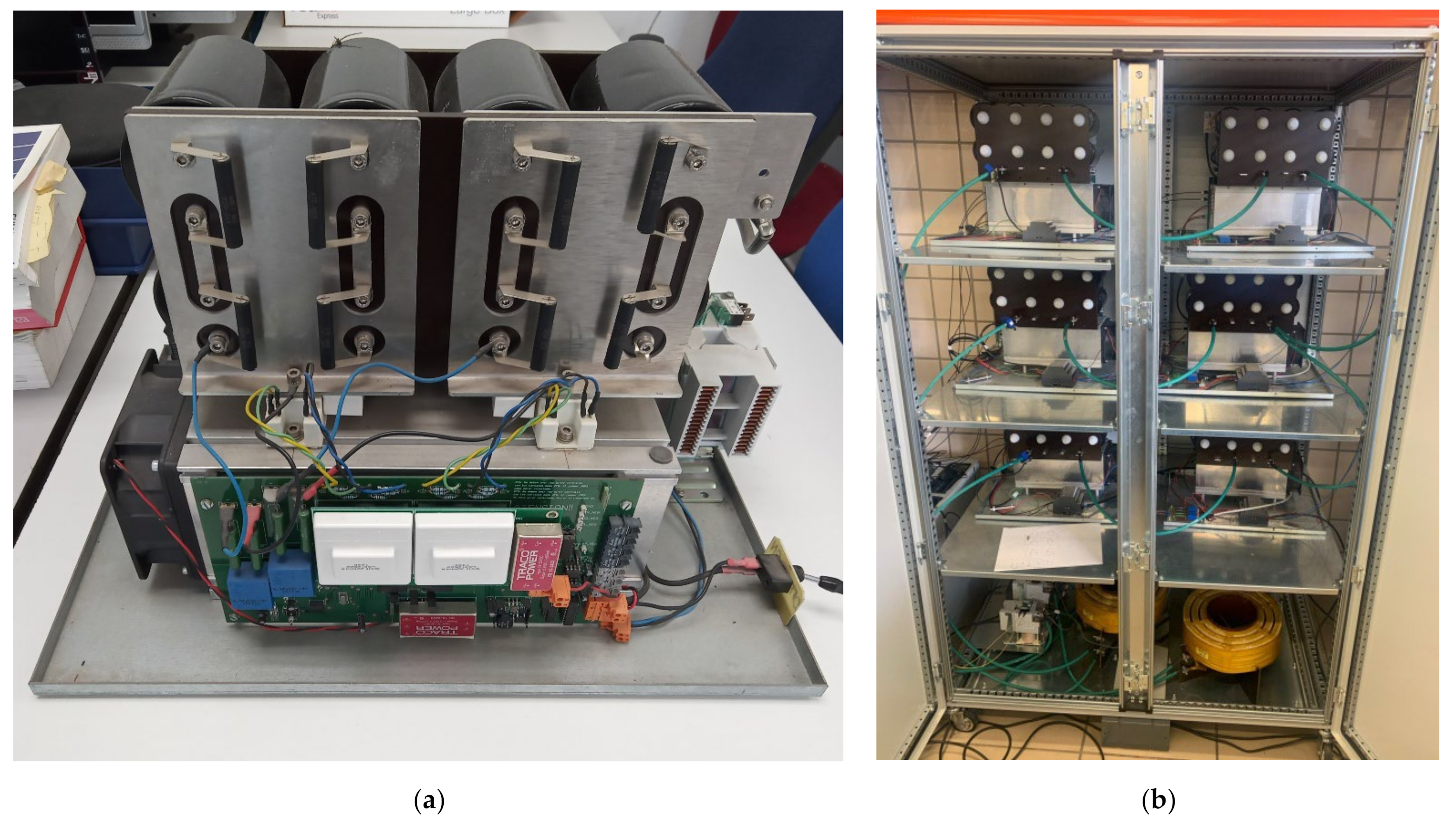
Figure 2a shows an individual H-Bridge module;
Figure 2b shows the whole converter, and
Table 1 shows the converter’s main characteristics.
The converter control hardware includes one local control unit per module plus a central control unit. Each local control unit consists of a Xilinx Spartan3A FPGA, the IGBT drivers, voltage sensors to measure the DC-link voltages, voltage and current sensors to measure the grid AC voltages and currents, and the necessary board for the signals’ adaptation. All local control units are connected to the central control unit by means of optical fiber, which ensures galvanic isolation between modules. The central control unit includes a Xilinx Spartan-6 FPGA that manages the communication with the other six local control units. It also includes a Texas Instruments eZdsp microprocessor, which runs the whole control method along with the current control layer. The microprocessor debug software is employed as human–machine interface to configure and run the tests.
The voltage and current measurement occur in the local control units, which are also programmed to send halt signals upon any DC-link overvoltage or driver error. This voltage, current and error information are sent to the central control unit, which acts accordingly. The control algorithm is run by the eZdsp microprocessor, though some modulation-related operations are run in parallel on the Spartan-6 FPGA to accelerate the process. When the new duty cycles have been calculated, they are sent to the local control units. This information is sent to all the modules at the same time, and the local control units use it as a synchronization signal to prevent their triangular carriers from deviating from one another. Finally, the local control units compare the corresponding duty cycle with a symmetric triangular carrier and activate the IGBTs accordingly.
The control cycle occurs twice per period of the triangular carrier. Due to the communication protocol followed by the local and central FPGAs, the activation of the IGBTs occurs a whole period of the triangular carrier after the voltage and current measurement. The central control unit considers this delay when controlling the currents.
The converter is connected to a California Instruments MX30 laboratory source. This source is configured to emulate a 400 V and 50 Hz grid. The reactive power exchanged with the source was 5 kVAr on all the tests.
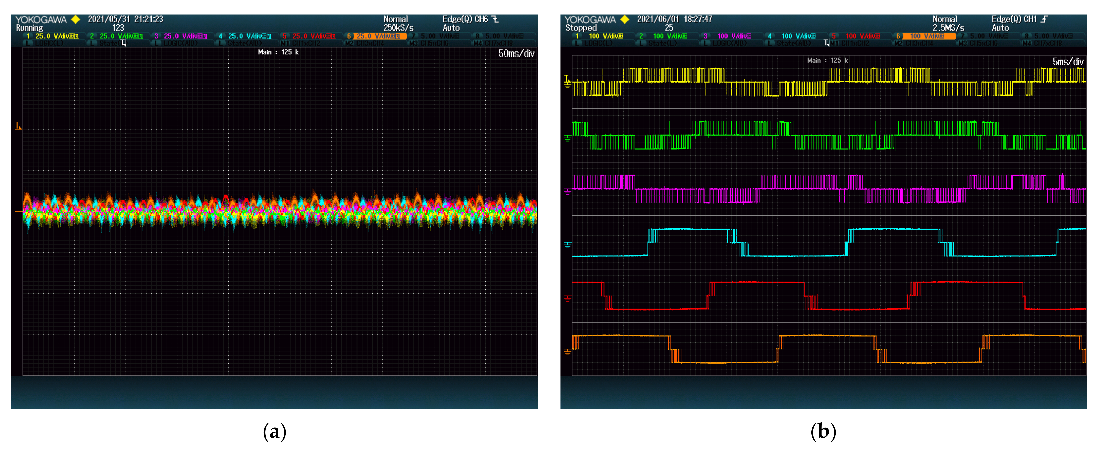
A Yokogawa DLM4058 oscilloscope was employed to measure the DC-links voltages () and the modules commutations. Therefore, each test is run twice, with the oscilloscope connected first to the DC-links and then to the modules’ output.
3.2. Methods
In order to clarify the context in which the proposed method is run,
Figure 3 shows a scheme of the general control method used during the tests. As mentioned in
Section 2, the method from [
34] and the proposed upgrade are applied in the modulation layer. The different parts of this control scheme are described below.
The left side of
Figure 3 shows how the power reference
is obtained. The voltage set points for all the modules DC-links voltages
are provided by the user and employed to calculate the desired total energy
to be stored in the converter. For the tests performed for this paper,
was set to 200 V for each module. The actual energy
stored by the modules is calculated from the measured DC-link voltages
. A PI regulator receives the energy error and selects the reference for the total active power
to be received by the converter.
A set point was manually selected for the reactive power
, which for all the tests performed for this paper was 5 kVAr. The active and reactive power set points (
and
) are provided to a current regulation layer, along with the measured grid voltages
and currents
. The current regulation layer, located in the middle of
Figure 3, selects the necessary phase voltages (
,
and
) for the converter to exchange the desired active and reactive power. A typical dq approach was used, with the d axis aligned with the voltage of the grid. The desired current d and q components were calculated from the power set points and controlled through PI regulators. The resulting phase voltages (
,
and
) passed to the modulation layer.
The modulation layer consists of the upgrade proposed in this paper. As stated in
Section 2, this method is configured using the gains
,
and
. Gain
is responsible for the modules DC-link voltages
to follow their set points
. Gain
is responsible for the DC power following and ripple reduction. No individual power references are necessary, as the converter does not include batteries or ultracapacitors. Thus, gain
only affects the DC-link voltage ripple: the greater
is for a module, the lower its ripple is expected to be. Finally, gain
is responsible for avoiding the aforementioned transition commutations. The greater
is for a module, the lower its effective switching frequency is expected to be. If
is set to 0 in all modules, the method behaves as in [
34] and can be used for comparison. During the tests,
is set to 1 in all modules.
and
are set independently for each module and are different on each test.
The method applied in the modulation layer includes the following steps:
- 4.
Update for the next control cycle as in (26).
The initial value of is 0 for all modules. Once the desired output voltages are obtained for all modules, the corresponding duty cycles are calculated and sent to the local control units. Finally, the duty cycles are applied, and the modules’ output voltages are obtained by means of PWM.
4. Tests and Results
The results of six tests are shown in this section. For all tests, the DC-links are first precharged by leaving all IGBTs open, then gains (
,
and
) are configured, and the reactive power reference is set to 5 kVAr (capacitive). A ramp reference is given to all DC-link voltages until their final set point is 200 V for each DC-link. Once a permanent state was reached, a screenshot of the oscilloscope was taken. For coherence, each module is always assigned the same color on the oscilloscope screen. These colors are shown in
Table 2.
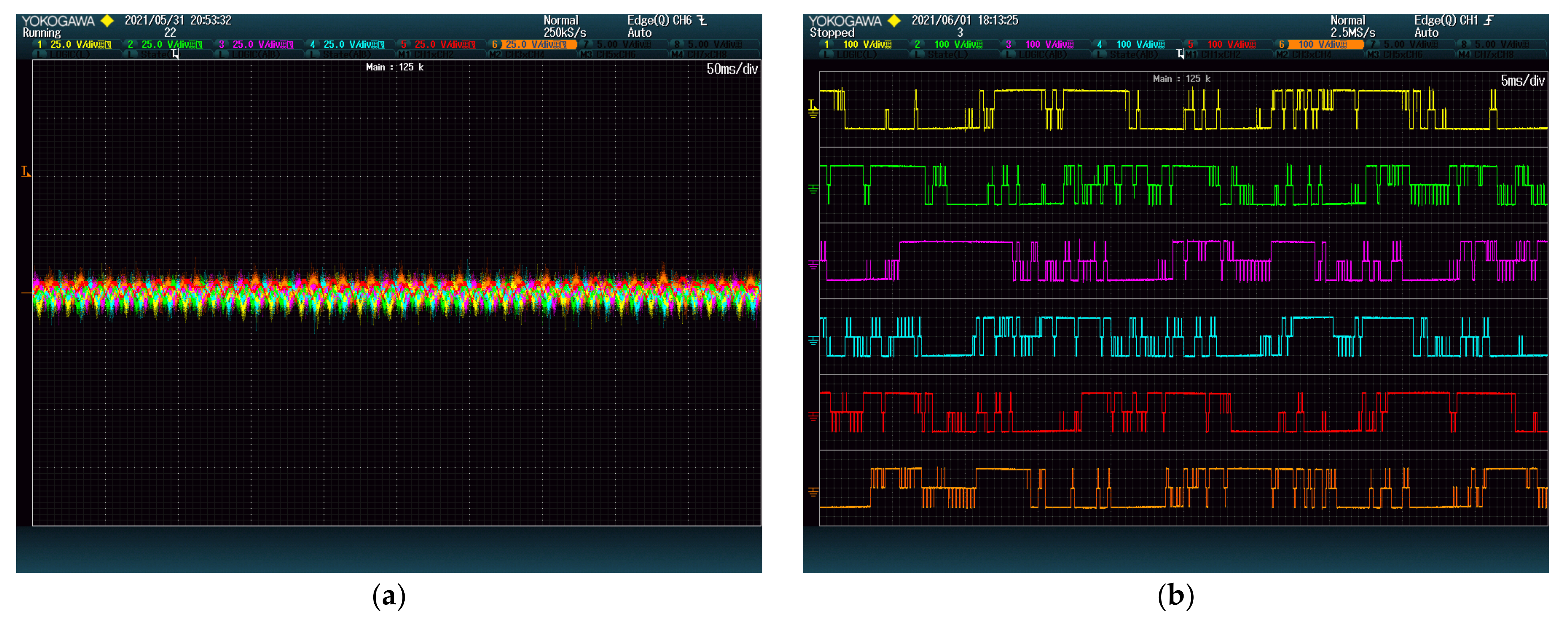
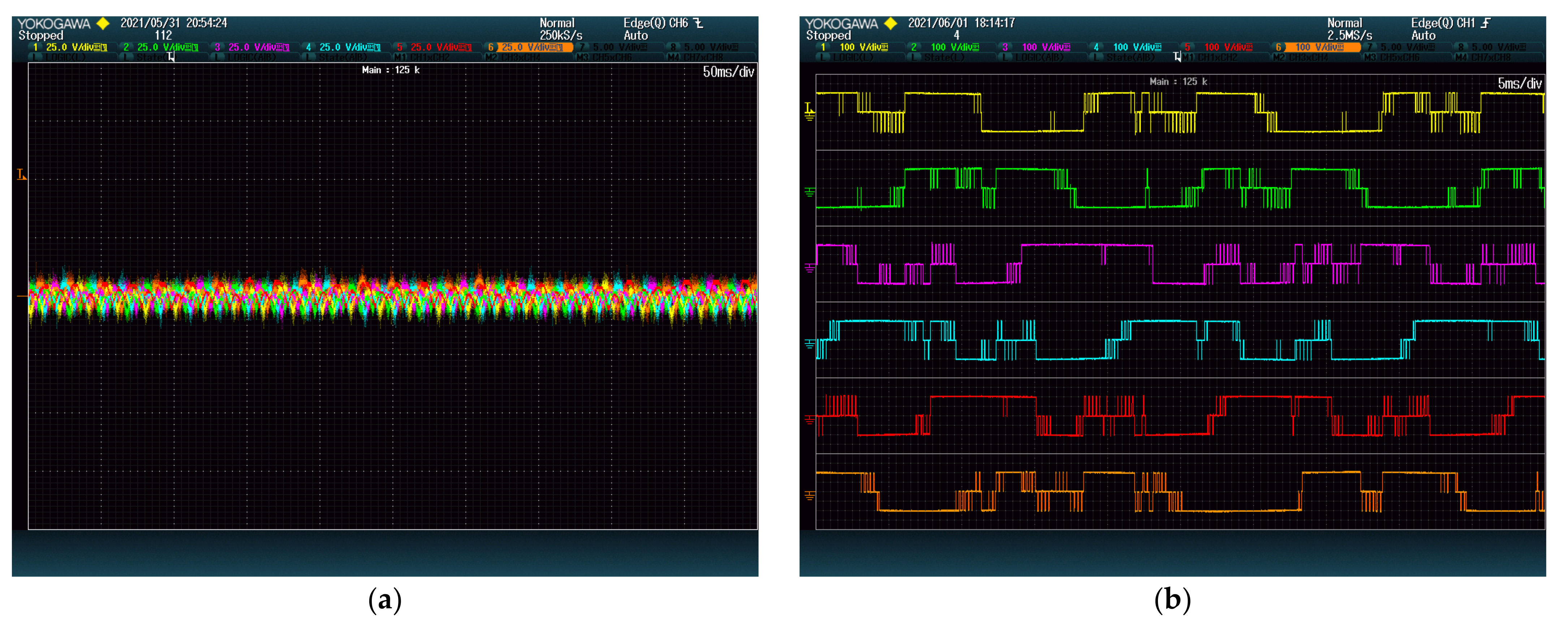
The first test simply intends to check the behavior of the original method from [
34] without any upgrade. In this way, it is possible to compare the performance of the proposed upgrade with the original method. In this first test,
is set to 1, whereas
and
are set to 0, so the optimization method only searches for DC-link voltage balance. The results of this test are shown in
Figure 4, including DC-link ripple and modules output.
The DC-link average voltage ripple is 13 V, and there are several commutations distributed among all the modules. The high switching frequency obscures the modulated wave shape, although it is possible to see when the output of each module is mostly high or mostly low. In many cases, the modulation is more similar to bipolar modulation than to unipolar modulation; the blue and green lines show good examples. This type of modulation is generally undesirable because it produces more transistor commutations and poorer current quality than unipolar modulation.
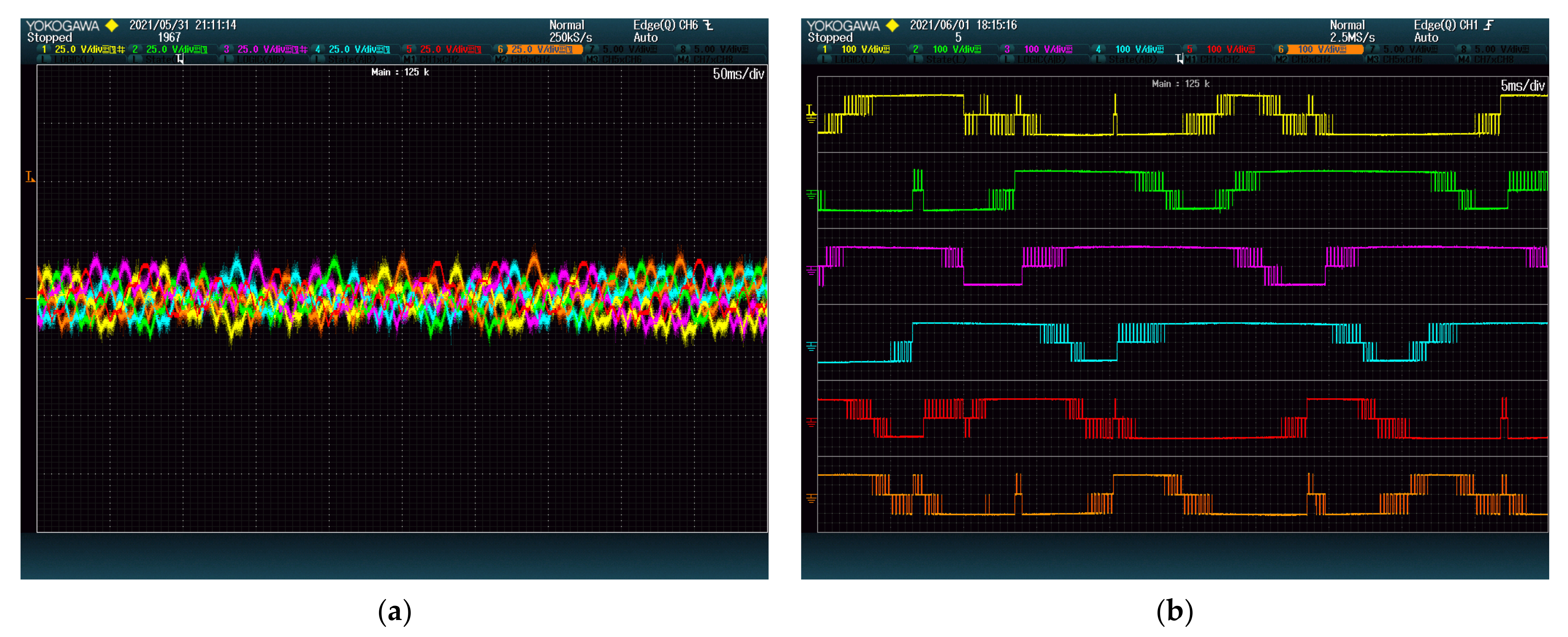
The second test aims to improve the previous result using the proposed upgrade. In particular, by selecting
for all modules, a small weight was given to the proposed partial objective function. The results are shown in
Figure 5.
The DC-link ripple is not significantly greater than in the previous test. The number of commutations decreased, and the modulation was then closer to unipolar. In general, the results of the second test are better than those of the first.
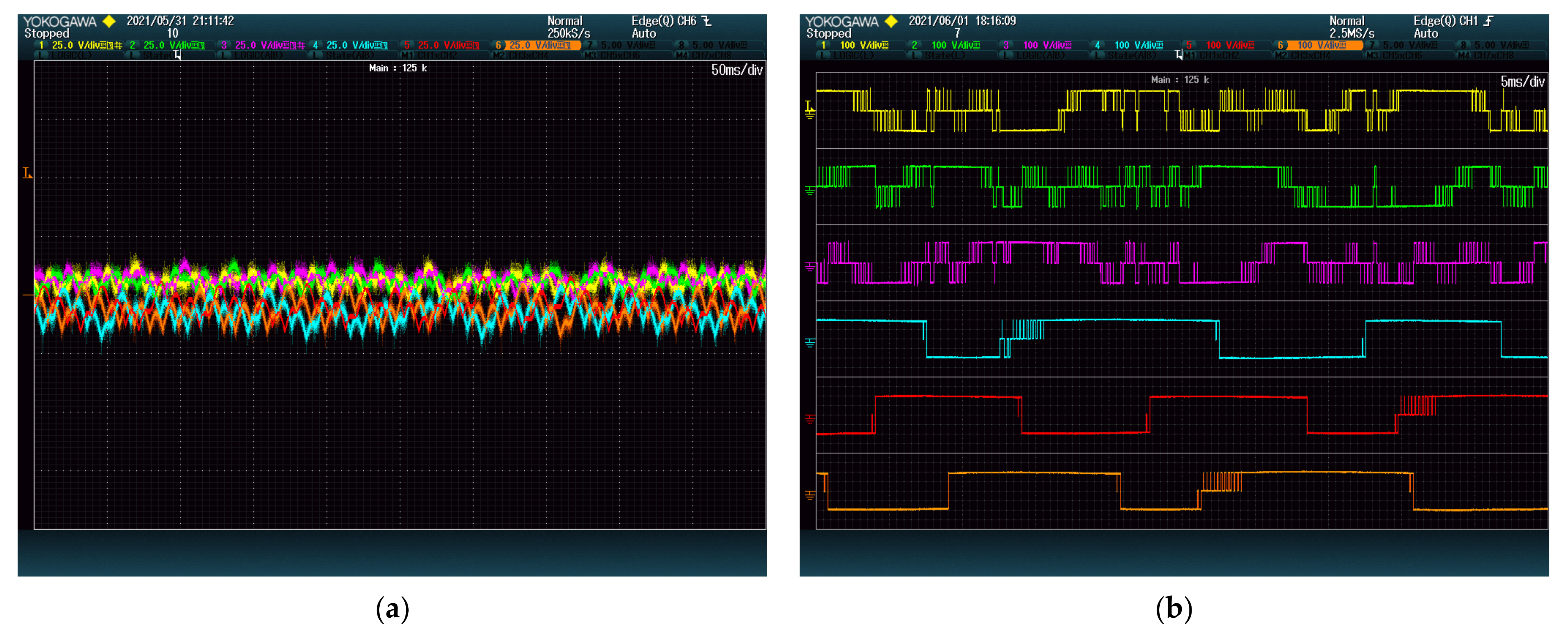
On the third test,
was increased to 0.1, producing the results shown in
Figure 6. The voltage ripple was about 31 V, more than double that in the previous two tests. The modulation is now almost only unipolar, with each module output clearly indicating the shape of the voltage wave.
Similar to a level-shifted PWM, only one module commutes in each phase, while the other remains saturated. One module of each phase produces the positive voltage (yellow, red and orange lines), whereas the other produces the negative voltage. In addition, only two modules remain nonsaturated at any given time. This indicates that the algorithm is using common-mode voltage to avoid switching several modules at a time.
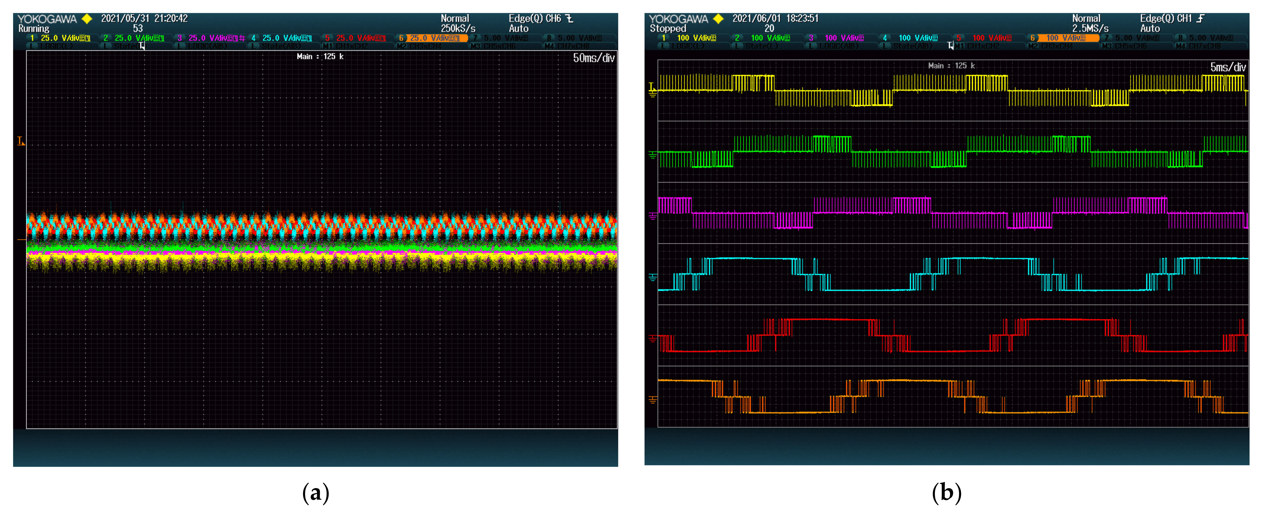
On the fourth test,
was set back to 0 for one module on each phase (yellow, green and purple lines). For the other modules,
retained its value of 0.1. Thus, switching was penalized only for one module per phase (blue, red and orange lines). The results are shown in
Figure 7.
As expected, the number of commutations is minimal in the modules where switching is penalized. Modulation is performed mainly by the other modules. Regarding the DC-link voltage, modules with penalized switching have 22.5 V ripple, whereas the other modules have about 13 V ripple, similar to the first test. However, treating the modules differently also produces some unbalance. The modules with switching penalty oscillate around 195 V, whereas the other modules have approximately 205 V on average.
The original method from [
34] also had the possibility of dealing with each module differently. In particular, for an application where the low ripple is more important for some modules and a low number of switching is important for other modules, a nonzero value of
could be given to the former. This configuration penalizes the ripple on some modules, forcing them to concentrate on the commutations.
This was tested in test number five for comparison. In particular,
was set to 0.1 for three modules (yellow, green and purple) and to 0 for the other modules.
was set to 0 for all modules, thus deactivating the proposed upgrade. The results are shown in
Figure 8.
When comparing the results from the fourth and fifth tests, the former was shown to produce less switching, whereas the latter produces a lower ripple. The fifth test also produces some unbalance in the opposite direction than the previous test.
The final test combined the settings of the previous two tests. In each phase, the ripple was penalized in one module (
) and the switching was penalized in the other module (
). This test searches for the combined advantages of the previous two. The results are shown in
Figure 9.
As shown, the result of both types of penalizations (ripple and switching) combined to produce a better result than any of them separately. Modules with switching penalization have the same or fewer commutations than in test number 4. The ripple in said modules is similar to the ripple they had in tests 1 and 2. The other modules have a very low ripple, similar (though not as low) as they had in test number 5. More importantly, the imbalance was corrected.
Table 3 shows the ripple amplitude of each DC-link for each test. These values were obtained from the figures shown in this section and correspond to the difference between the maximum and minimum voltages shown in the figures.
The effective switching frequency experienced by the transistors is given in
Table 4. These values were obtained by counting the number of times that each module changes state in the figures. Please note that a 1 Hz frequency would mean that each transistor of the module opens and closes once per second. The maximum possible switching frequency is the triangular carrier frequency (i.e., 2 kHz). For comparison, the transistor switching frequency would be 2 kHz on a phase-shift PWM and 1 kHz on a level-shifted PWM.
During the tests, the phase current wave was checked using a grid analyzer. No significant changes were found between the current wave and that of [
34]. This only signifies that the achieved switching reduction had no impact on the phase currents.
5. Discussion
The first test already shows a lower average switching frequency (918.33 Hz) than the corresponding level-shifted PWM. This occurs because the original method from [
34] is allowed to use a common-mode voltage. In that case, the theoretical limit for the effective switching frequency would be 666.67 Hz instead of 1 kHz because only two modules (instead of three) need to use PWM on each control cycle.
On the second test, the effective switching frequency is reduced to an average of 789.16 Hz. This means that the proposed upgrade produces 14% fewer commutations than the original method from [
34]. It should be noted that 14% fewer commutations do not mean 14% fewer switching losses. As previously stated in
Section 2, the method selectively avoids the commutations that would produce the most losses but allows commutations on phases whose current is low. Thus, the switching losses are reduced by more than 14%.
In addition, the ripple does not increase significantly compared to the previous test. According to (16), the ripple produced by the switching avoidance should be about 1% of the DC-link voltage. Since the desired DC-link voltages are set to 200 V, this ripple should be about 2 V. The extra ripple measured is 0.83 V, which is insignificant compared to the original 13 V ripple. No current distortion was found during the second test, so it can be said that the method would save more than 14% of the switching losses with practically no drawback.
The third test shows that the method can reduce the effective switching frequency to an average of 714.16 Hz. This corresponds to a 22% reduction in commutations with the respective reduction of the switching losses. However, this time, there is a drawback in the form of the DC-link ripple. According to the estimation given by (16), the ripple produced by the upgrade would be on the order of 20 V, which roughly corresponds to an increase in the ripple compared to the first test. This test validates the formula as an estimation.
For a STATCOM, where voltage ripple is expected on the capacitors, it is important to consider whether it is preferable to have the extra ripple on the capacitors or the extra switching on the transistors. With the proposed method, it is now possible to simulate the whole Pareto frontier and design the STATCOM accordingly. Once built, it is still possible to adjust the position in the frontier by shifting the value of . The proposed method gives a wider range of choices in this respect.
For other applications, such as photovoltaic generation or energy storage (with batteries or ultracapacitors), the ripple is undesirable. Photovoltaic applications require stable DC voltage for maximum power point tracking, and batteries and ultracapacitors would consume small fractions of charge cycles due to the current ripple. Fortunately, the proposed upgrade was made compatible with the ripple reduction technique employed in [
34].
The results of the fourth, fifth and sixth tests show the interaction between both techniques (i.e., the original method from [
34] and the proposed upgrade). When comparing the combination of objectives to the switching reduction alone, it was found that the ripple decreases from 13 V down to less than 3 V on the desired modules. On the other hand, when comparing the combined techniques to ripple reduction alone, the total number of commutations is reduced by 20%. Moreover, the reduction of the effective switching frequency in the selected modules is greater than 66%.
The two techniques interact well together, correcting each other’s imbalance and reducing the ripple that the proposed upgrade would cause on its own. This shows that, in hybrid applications, the gains of each module can be tuned according to the module application.
Modules for reactive power compensation, whose DC-link typically includes only capacitors, can afford a higher ripple. In these modules, should be relatively high to ensure balance, and should be left null. , which is expected to have a medium value, can be selected according to the affordable extra ripple, possibly using the estimation given by (16);
Modules connected to photovoltaic panels cannot afford that much ripple. For these modules, is the most important gain and should have the highest value. As long as the ripple is small, a low value of may be acceptable. If the ripple is unacceptable, then a low value of may be used instead. It is also possible to leave both and to 0;
In modules with ultracapacitors, the DC-link voltage is more stable, but the ultracapacitors can suffer from the current ripple. In this case, must be null to prevent damage. should be the dominant gain to prevent current ripple and allow the module to respond quickly to power demand. should have a relatively low value, but it should not be null to prevent the ultracapacitors from discharging over time;
Finally, modules with batteries are typically controlled using power or current set points instead of voltage set points. is the appropriate gain for controlling such power or current reference. The other gains should be null.
On converters with a high number of modules, the proposed method may lead to the possibility of combining different transistor technologies, including even GTOs, as they would have about 50 Hz or 100 Hz effective switching frequency. The other modules may include IGBTs for general-purpose modules and MOSFETs for modules incorporating energy storage systems.


