Article

Partial Power Processing and Efficiency Analysis of dc-dc Differential Converters

by
Jéssika Melo de Andrade
*,
Roberto Francisco Coelho
and
Telles Brunelli Lazzarin
Electrical Engineering Department, Federal University of Santa Catarina, Florianopolis 88040-900, Brazil
*
Author to whom correspondence should be addressed.
Energies 2022, 15(3), 1159; https://doi.org/10.3390/en15031159
Submission received: 10 January 2022 / Revised: 2 February 2022 / Accepted: 2 February 2022 / Published: 4 February 2022

Abstract

:
This paper presents a partial power processing and an efficiency analysis of dc-dc differential converters based on the use of two basic converters of the same group: the positive or negative group. The paper contributes theoretical analysis and demonstrates that the differential converters based on the positive group process has more power than the load requires, and that the differential converters based on the negative group process has less power than the load needs. This is an important advantage of the negative group converters, since a parcel of the output power is directly transferred by the input source to the load, resulting in partial power processing. In order to verify the theoretical analysis herein developed, ten prototypes are evaluated considering an input voltage of 20 V and output power of 100 W.

1. Introduction

Environmental concerns and the search for the diversification of energy matrixes make renewable sources a real alternative for electrical energy production around the world [1,2]. Among these renewable sources, photovoltaic and wind are considered the most promising [3]. Unfortunately, these sources provide low output voltages when compared to the peak value of grid voltage, therefore high gain step-up dc-dc converters are required to efficiently comply with the requirements for grid connection [4]. In light of this, the literature has presented several topologies of high gain step-up dc-dc converters in the past few years [5,6,7,8,9,10,11,12,13,14,15,16,17,18,19,20,21,22].
Step-up converters are usually classified as isolated or non-isolated [7]. In the isolated topologies the gain is easily increased by the turn ratios of the transformer, however, the leakage inductance associated with the windings can cause high voltage peaks across the power switches. Therefore, techniques to reduce it must be implemented, which may degrade the efficiency [8].
Conversely, non-isolated topologies make use of techniques to increase the voltage gain [9], such as: switched capacitors and/or inductors cells [10,11,12,13], coupled inductors [14,15,16], cascaded and stacked connections [17,18], or a combination of them [10,11,12]. Switched and coupled inductors can also imply voltage spikes on the power switches, requiring clamping circuits or snubbers to smooth it. Switched capacitors are able of raising the voltage gain without inductances; moreover, the power switches can be subjected to high current peaks. Cascaded and stacked connections need a high number of components, which can reduce efficiency. Each of these techniques presents specific features, which have to be evaluated accordingly with the application [19].
Recently, non-isolated topologies based on the differential connections between basic converters were introduced by [19,20,21]. This kind of connection is composed of two stages and it provides higher voltage gain with a lower duty cycle value, which can improve efficiency when compared to a one-stage converter.
In [19,20] the differential connections are derived from two basic converters of different groups, classified as positive and negative. The converters of the positive group are those in which the input and output voltages have the same polarity to a common ground terminal. This group includes the buck, boost, SEPIC, and zeta converters. Conversely, in the converters of the negative group, the polarity of the input and output voltages are inversed in respect of this common terminal, as the buck-boost and Ćuk converters.
Whereas the authors of [19] derived the differential converters from two basic converters of the same group, the authors of [20] proposed the connection between converters of different groups. Nevertheless, both works approached these connections to provide high-gain step-up dc-dc converters, presenting several possible combinations of converters, detailing the modulations and control strategies, and deriving the static gain equations. Some of these differential converters were detailed in [10,22,23].
Particularly, in the differential converters based on conventional converters of the same group, the voltage of the input source contributes with the voltage applied to the load, which provides these differential converters the ability to accomplish Partial Power Processing (3P). In differential converters, 3P can be used to improve the global efficiency of this kind of connection. Additionally, 3P applied in dc-dc differential converters can be a strong argument to employ this solution rather than single-stage dc-dc converters, so that the 3P differential converters become natural candidates to be applied to renewable systems due to their improved efficiency [24,25]. It is important to highlight that differential converters can be employed in any application that requires a step-up power stage, such as photovoltaic, wind, and storage systems.
In the literature, the features related to partial power processing are still not formalized for differential converters. In [19], for example, the parcel of power delivered from the input source directly to the load was considered as part of the power processed by one of the basic converters. In light of this, this paper contributes with the detailing of how the power is distributed inside differential converters, in order to demonstrate their ability to provide partial power processing and to show how the total efficiency is impacted.

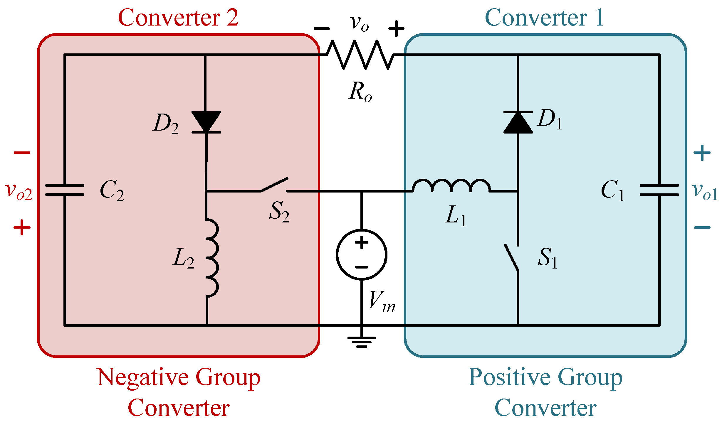
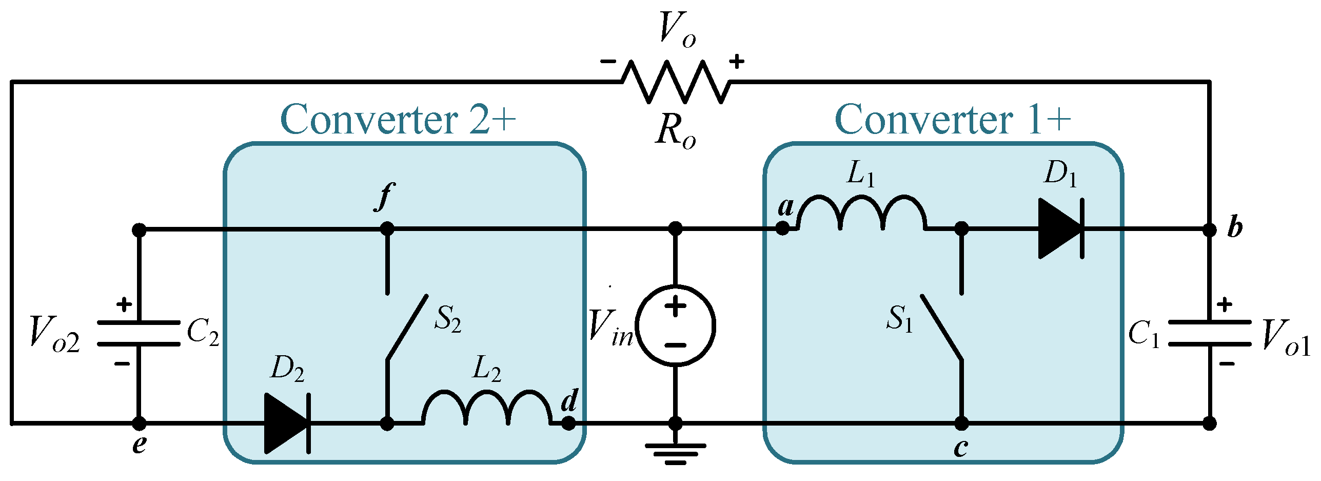
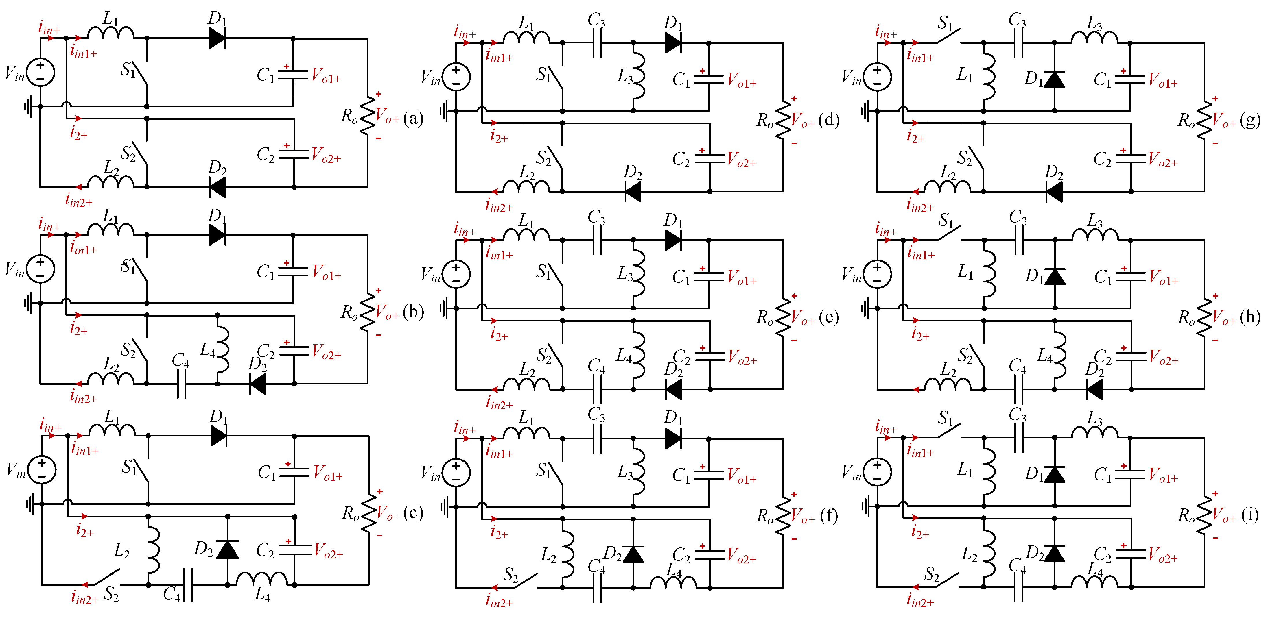
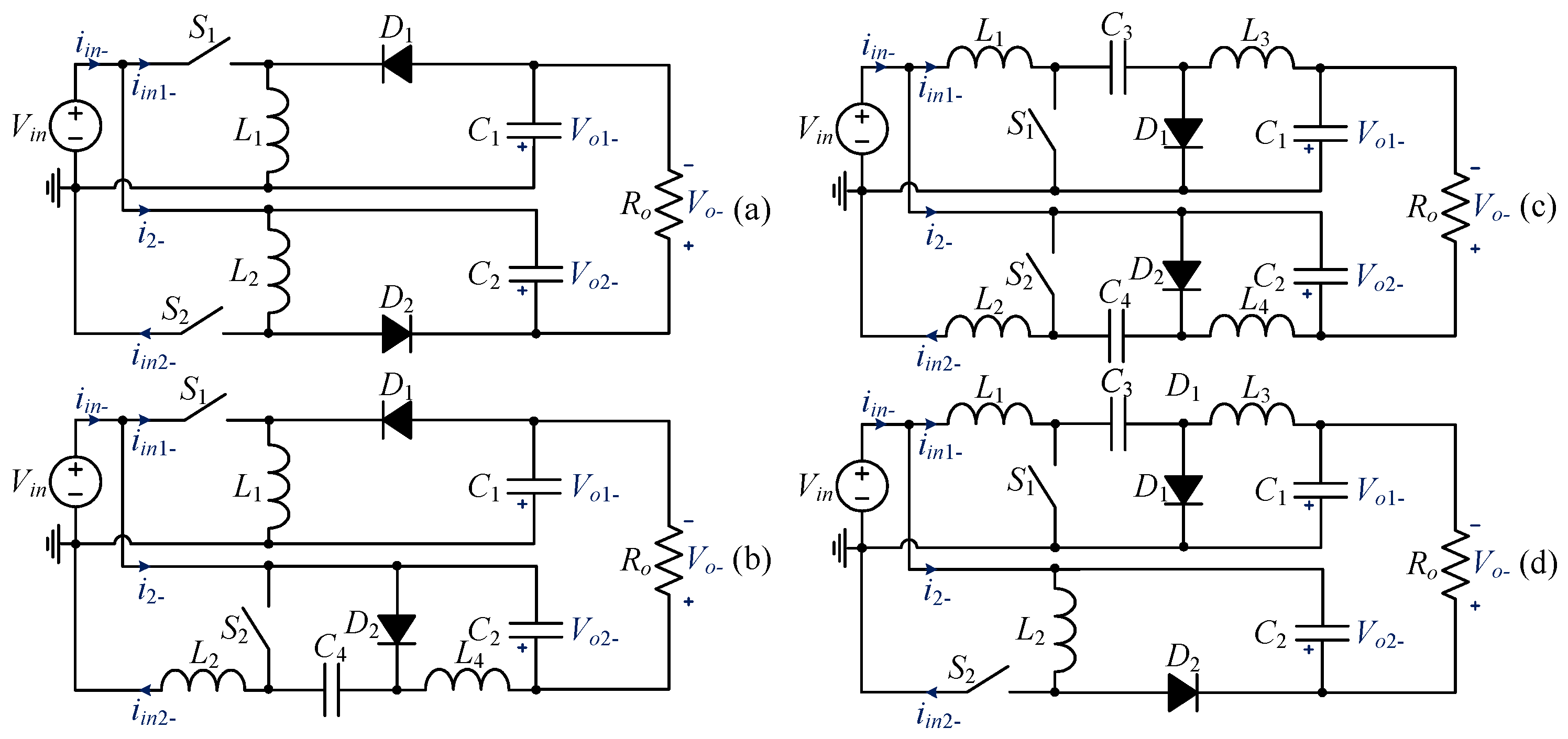
2. Brief Review of Differential Connections for Step-Up Converters

In [20] the differential connections are derived from two basic converters of different groups, so that the differential voltage is the sum of the output voltages of each of the basic converters, as shown in Figure 1, where a boost converter (positive group—Converter (1) is connected with a buck-boost converter (negative group—Converter (2). In this case, the differential voltage only depends on the output voltage of each basic converter:
Vo = Vo1 + Vo2.
As an alternative, [19] proposes a methodology to develop differential converters by the connection between basic converters of the same group (positive or negative). An example is exhibited in Figure 2 considering two boost converters (positive group), in which a conventional boost converter is connected with a “mirrored” boost converter. The “mirrored” boost shown in Figure 2 is defined in [19] and it is also named in the literature as a floating-output boost converter [26,27]. The differential connection of two boost converters is already known in the literature either as floating-output double-boost converter [26,27] or traditional double dual boost converter [28,29]. A generalization for any converter type is shown in Figure 3.
On analyzing the circuit shown in Figure 3a, the differential output voltage can be written as:
V o + = V o 1 + + V o 2 + V i n .
Furthermore, if the both basic converters belong to the negative group, as illustrated in Figure 3b, the differential output voltage can be described as:
V o = V o 1 + V o 2 + V i n .
On analyzing (2) and (3), it is possible to verify that the input source (Vin) contributes with the differential voltage applied to the load, respectively decreasing and increasing it. This conclusion is highlighted in Figure 4. In the positive group, the converters process more power than the load needs due to the decreasing of the input voltage as shown in Equation (2). However, in the negative group, there is partial power processing since the input voltage directly delivers a part of the output power to the load, which is the main topic addressed in this paper, as discussed in detail in Section 3.
Based on Equations (2) and (3), the static gains of the differential converters respectively derived from basic converters of the positive and negative groups can be written as:
V o + V i n = G C C M + = G C C M 1 + + G C C M 2 + 1 ,
V o V i n = G C C M = G C C M 1 + G C C M 2 + 1 .
where the static gain of each basic converter in continuous conduction mode (GCCM1+, GCCM2+, GCCM1− and GCCM2−) can be individually obtained by the conventional analysis.
The input current resulting of the differential connection of basic converters of the positive group (iin+) is:
i i n + = i i n 1 + + i 2 + .
where:
i 2 + = i i n 2 + i o +
Replacing (7) in (6), results in:
i i n + = i i n 1 + + i i n 2 + i o + .
If basic converters of the negative group are considered, the input current (iin+) is:
i i n = i i n 1 + i 2 .
where:
i 2 = i i n 2 + i o .
Replacing (10) in (9), results in:
i i n = i i n 1 + i i n 2 + i o .
Equations (8) and (11) are important figures of merit used to analyze the experimental results presented in Section 4.

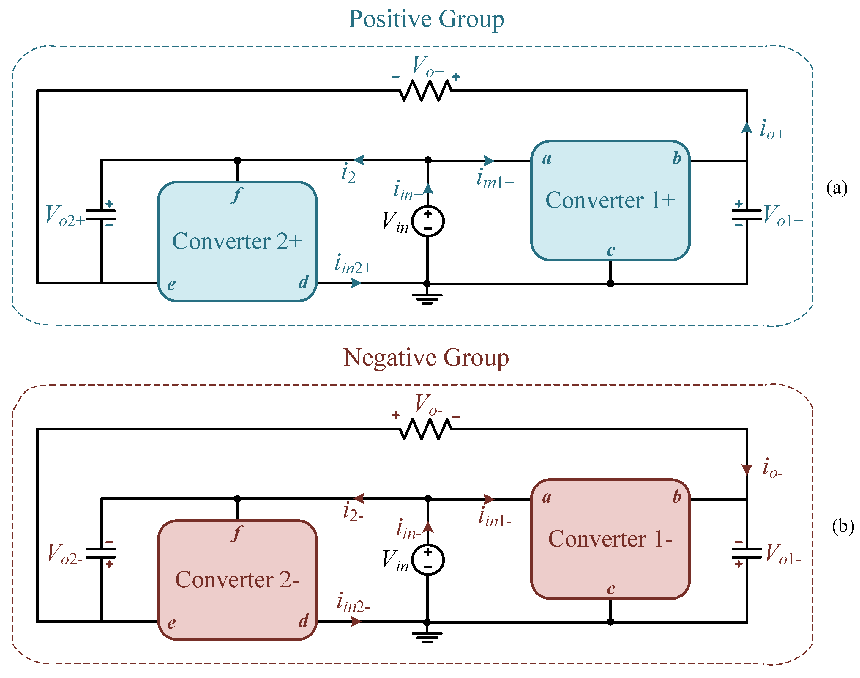
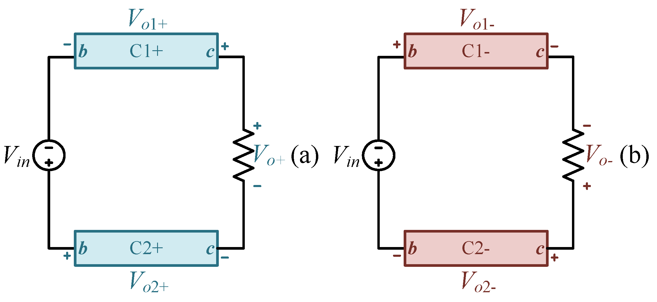
3. Partial Power Processing and Efficiency Analysis

Both connections shown in Figure 3 are herein analyzed from the equivalent circuits shown in Figure 4.
In the differential connection of basic converters of the positive group (Figure 4a) the input voltage (Vin) is negative and contributes to decreasing the differential output voltage (Vo+). It results in the circulation of non-active power [25] through the differential converter but does not imply the direct transfer of power from the input to the output. In light of this, to compensate for the reduction of the differential output voltage caused by the input voltage, the Converters 1+ and 2+ need to process more power than the load requires.
Conversely, in the differential connection of basic converters of the negative group (Figure 4b) the input voltage (Vin) is positive and contributes to increasing the differential output voltage (Vo). As a consequence, a parcel of the power supplied by the input source is directly transferred to the load. Hence, Converters 1− and 2− need to process less power than the load requires, which is the main feature expected from the 3P converters.
The percentage of power processed by each of the basic converters in the differential connection of the negative group can be defined in terms of static gain, as:
P 1 ( % ) = P 1 P o = V o 1 I o V o I o = G C C M 1 G C C M ,
P 2 ( % ) = P 2 P o = V o 2 I o V o I o = G C C M 2 G C C M ,
P s o u r c e ( % ) = P o P 1 P 2 P o = 1 ( G C C M 1 + G C C M 2 G C C M ) .
where, P1−(%) and P2−(%) are the percentage of power processed by Converter 1− and Converter 2−, respectively, and Psource is the percentage of power processed by the input source.
Equations (12) and (13) are also valid to describe the differential connection from positive group converters, however, in this case, the percentage of power processed by the input source (Psource+(%)) is given by:
P s o u r c e + ( % ) = P s o u r c e ( % ) .
The power delivered to the load in the positive group is given by:
P o ( % ) = P 1 + ( % ) + P 2 + ( % ) P s o u r c e + ( % ) ,
whereas, for the negative group, it is defined by:
P o ( % ) = P 1 ( % ) + P 2 ( % ) + P s o u r c e ( % ) .
Accordingly, with Equations (12)–(15), it is possible to define the amount of power processed by the basic converters employed in a differential connection, as summarized in Table 1. This table is assembled considering equal duty cycles for driving both of the basic converters, that is, D = D1 = D2.
The results obtained in Table 1 are graphically represented in Figure 5 together with the experimental points acquired from the prototypes approached in Section 4. Additionally, the converters of positive and negative groups of Table 1 are exposed in Figure 6 and in Figure 7, respectively. All the practical tests were evaluated at rated power (100 W) under an input voltage (Vin) of 20 V. Figure 5a–c show the results related to the differential connection of positive group converters whereas Figure 5d depicts the results related to the differential connection of negative group converters.
Figure 5a presents the theoretical curves and experimental points for the connection between the boost and the mirrored boost converters. In the entire range of duty cycles, both converters process the same amount of power. As one can note, the sum of the power processed by each basic converter is higher than the power delivered to the load. For example, considering D = D1 = 0.7, the boost and the mirrored boost converters process each one 60% of Po and the input voltage is responsible for 20% of Po. This result corroborates the theoretical analysis previously presented. Replacing these values in (16), the output power is:
P o ( % ) = 60 % + 60 % 20 % = 100 % .
The theoretical curves for the connection between the boost and the mirrored SEPIC converters are exhibited in Figure 5b. These curves are also valid for the connections between the boost and the mirrored zeta converters and between the SEPIC or zeta and the mirrored boost converters. The experimental points herein presented were acquired considering the boost and the mirrored SEPIC converters. In this connection, the SEPIC converter processes 50% of Po independently of the duty cycle value and its position in the differential connection (as Converter 1 or 2). On the contrary, as is evidenced in Table 1, the power processed by the boost converter (mirrored or not) varies accordingly to the duty cycle value. For example, with D = 0.7, the boost converter processes 75% of Po and the input voltage decreases Po by 25%.
Figure 5c presents the curves for the connection between the SEPIC and the mirrored Zeta converters. Both of them process the same power in all ranges of the duty cycle and like in the other positive group connections, the input voltage reduces the output power. The experimental data shown in Figure 5c is also valid to represent the connections between the Zeta and the mirrored SEPIC converters or between the Zeta or SEPIC and the mirrored SEPIC converters.
For the connections between the boost and the mirrored SEPIC converters or between the Zeta and the SEPIC converters or still between the Zeta and the mirrored SEPIC or Zeta converters (Figure 5b,c), the minimum duty cycle is 0.5, in order to avoid that these converters process more than 100% of Po. It is worth mentioning that in the positive group connections the influence of the input voltage on the differential voltage decreases as the duty cycle increases. Thus, the positive group connections are more attractive for high-gain applications.
The curves related to the negative group converters are represented in Figure 5d. Unlike the positive group converters, now the input voltage is summed to the output voltage of each basic converter, which processes less power than the load requires. As an example, for a duty cycle of 0.7, each of the basic converters process 40% of Po and the input voltage contributes with the remaining 20% to feed the load. Replacing these values in (17):
P o ( % ) = 40 % + 40 % + 20 % = 100 % .
The curves plotted in Figure 5d were experimentally verified, considering the connection between the Ćuk and the mirrored Ćuk converters.
Among the connections presented in Table 1, the only topologies in which the Converters 1 and 2 process different power levels are those composed of a boost and a mirrored SEPIC converter or between a boost and a mirrored Zeta converter. It is important to mention that these converters can also process the same power levels if the duty cycle values used to drive them are adjusted to be different. In light of this, in order to provide the power balanced between the converters, the duty cycle D2 applied to the Converter 2 can be written in function of the duty cycle D1 applied to the Converter 1, as:
| G C C M 1 + | = | G C C M 2 + | 1 1 D 1 = D 2 1 D 2 D 2 = 1 2 D 1 .
Therefore, for D1D2, the static gain and power processed by each converter are given by:
G C C M + = 1 + D 1 1 D 1 ,
P 1 + ( % ) = P 2 + ( % ) = 1 D 1 + 1 ,
P s o u r c e + ( % ) = 1 D 1 1 + D 1 .
Equations (22) and (23) are plotted in Figure 8 together with the experimental points obtained by the experimentation of a differential converter prototype based on the boost and mirrored SEPIC converters. It should be verified that these results are similar to those presented in Figure 5a.
On evaluating the power levels processed by each converter, the efficiency of the positive (n+(%)) and negative group converters (n−(%)) are:
n + ( % ) = P 1 + ( % ) n 1 + ( % ) + P 2 + ( % ) n 2 + ( % ) P s o u r c e + ( % ) n s o u r c e + ( % ) ,
n ( % ) = P 1 ( % ) n 1 ( % ) + P 2 ( % ) n 2 ( % ) + P s o u r c e ( % ) n s o u r c e ( % ) .
where n1+(%) and n1−(%) are the efficiencies of the Converter 1+ and Converter 1−, n2+(%) and n2−(%) are the efficiencies of the Converter 2+ and 2−, and nsource+(%) and nsource−(%) are the efficiencies of the input sources.

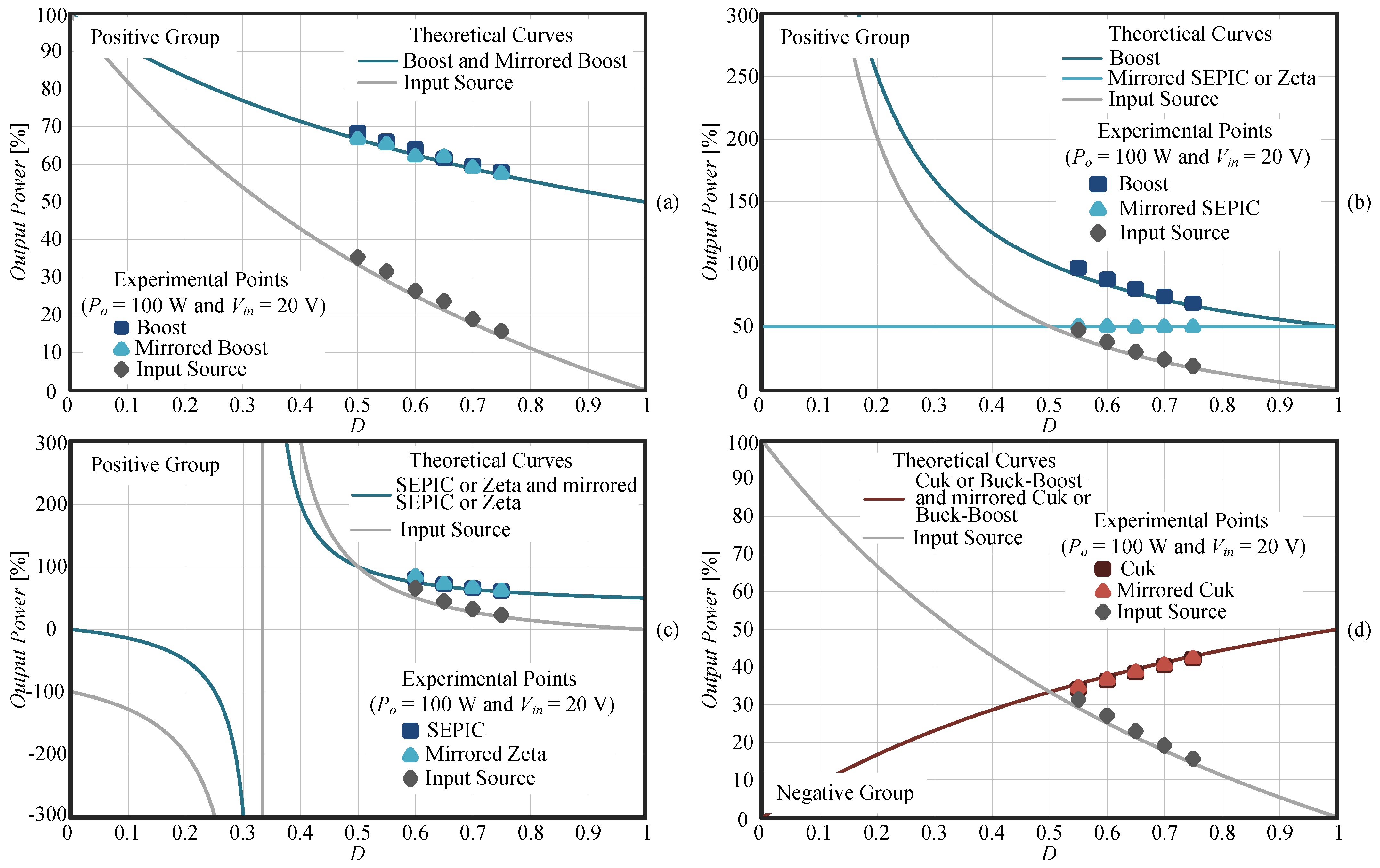
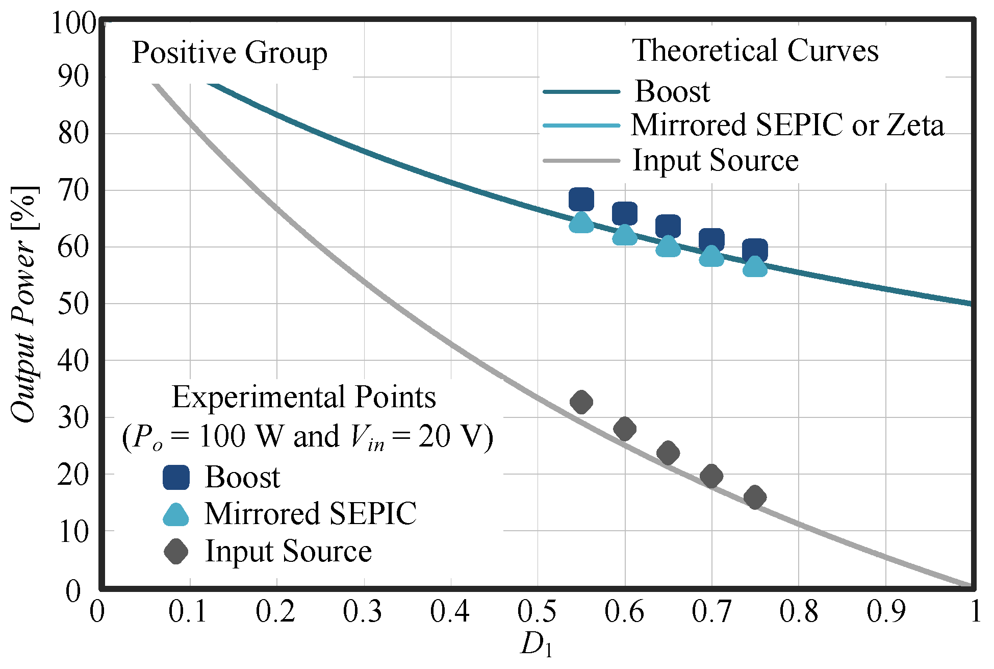
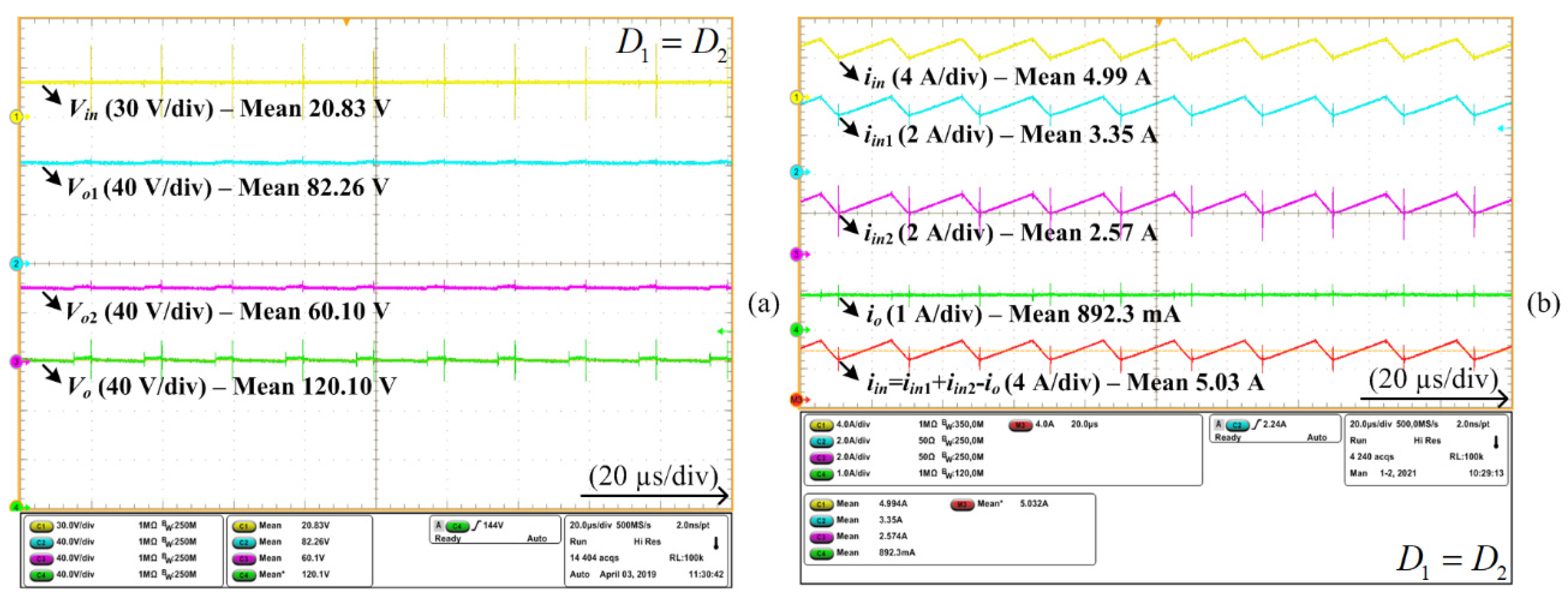
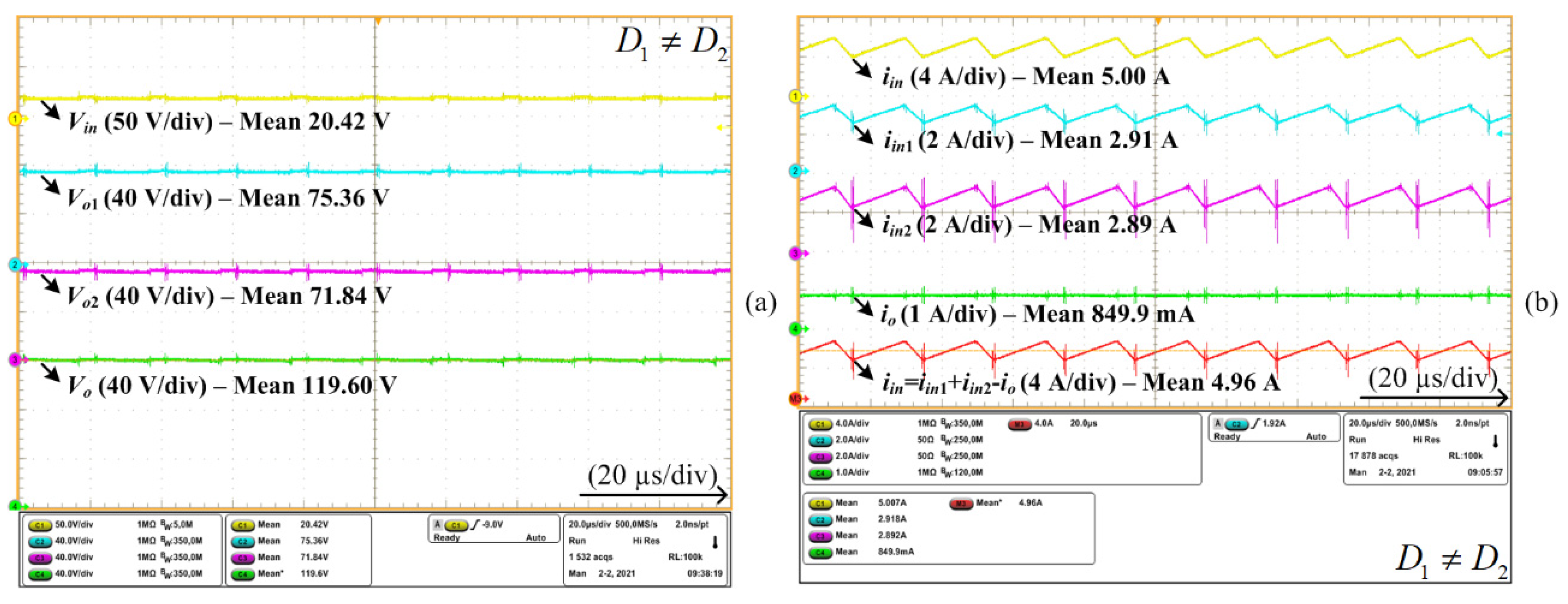
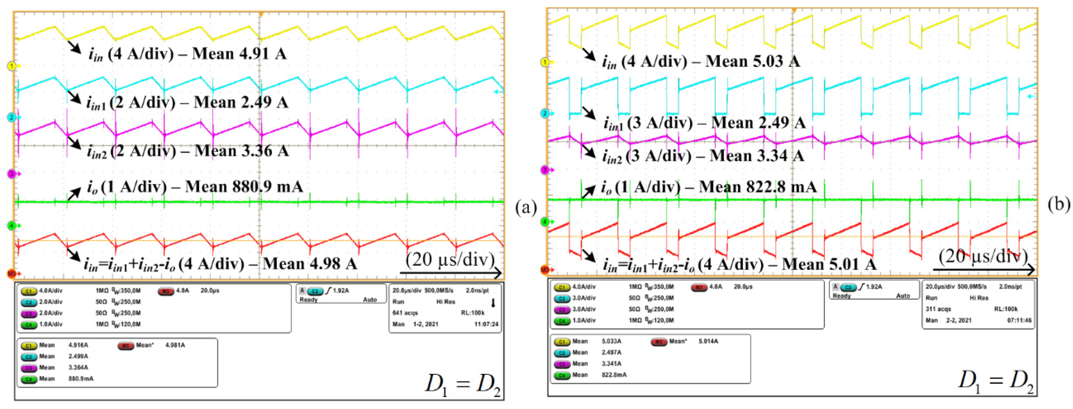
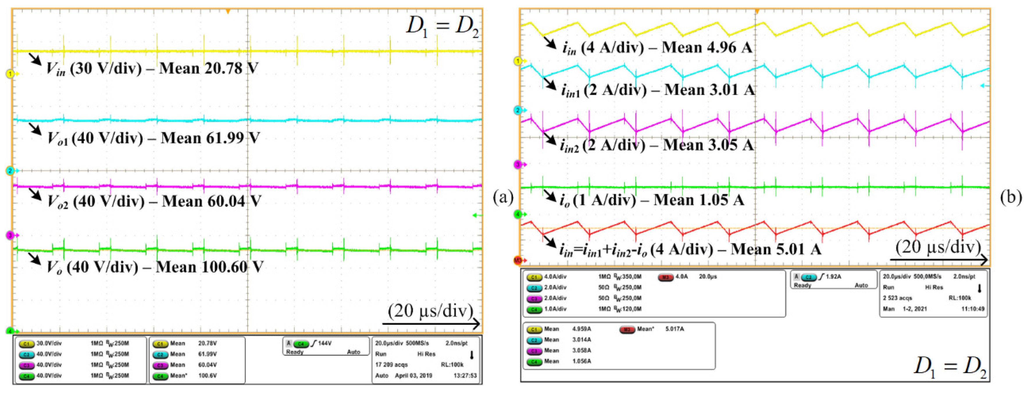
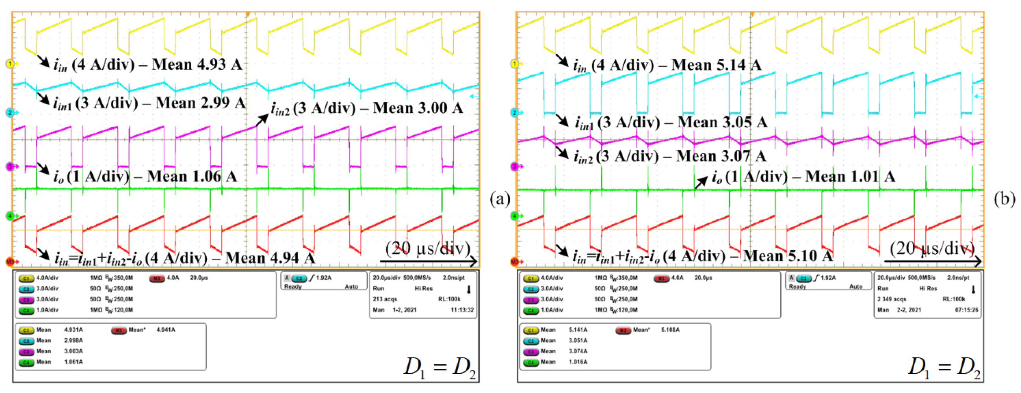
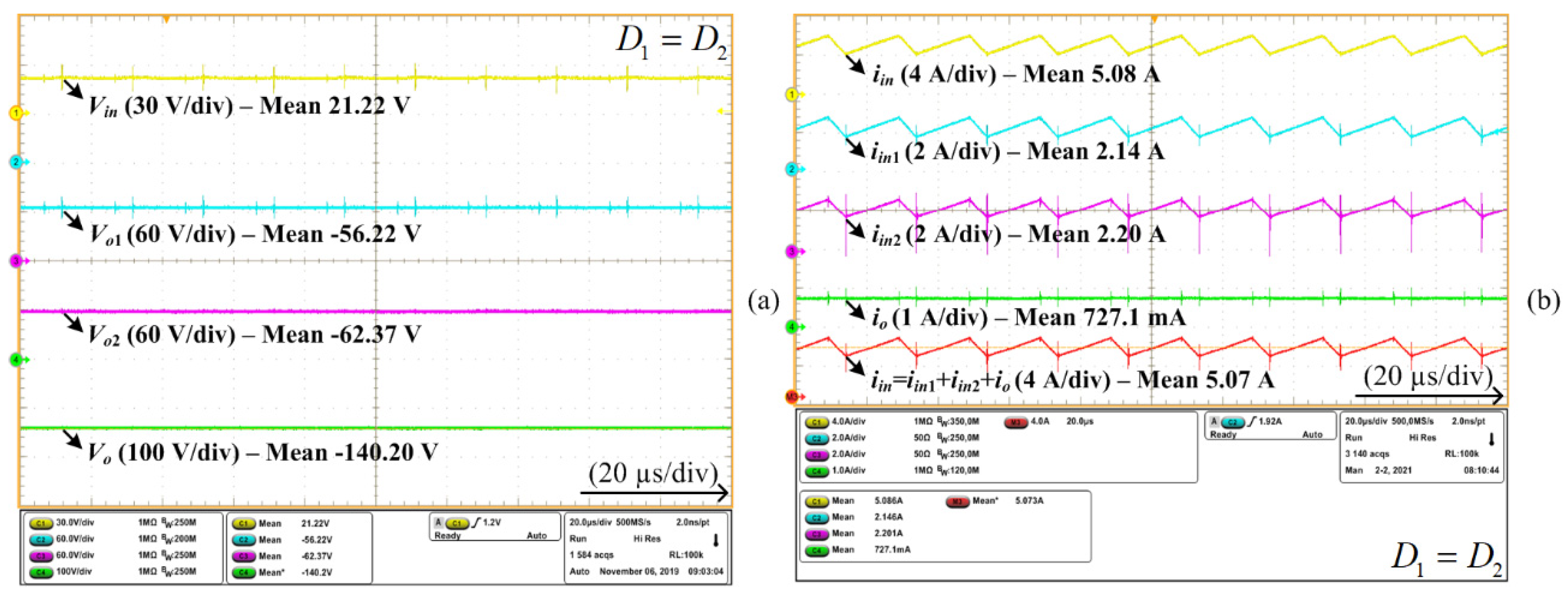
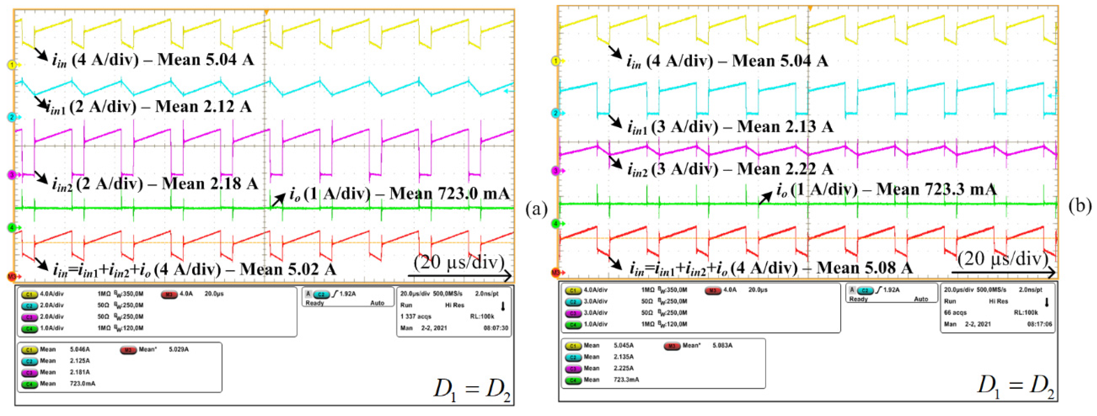
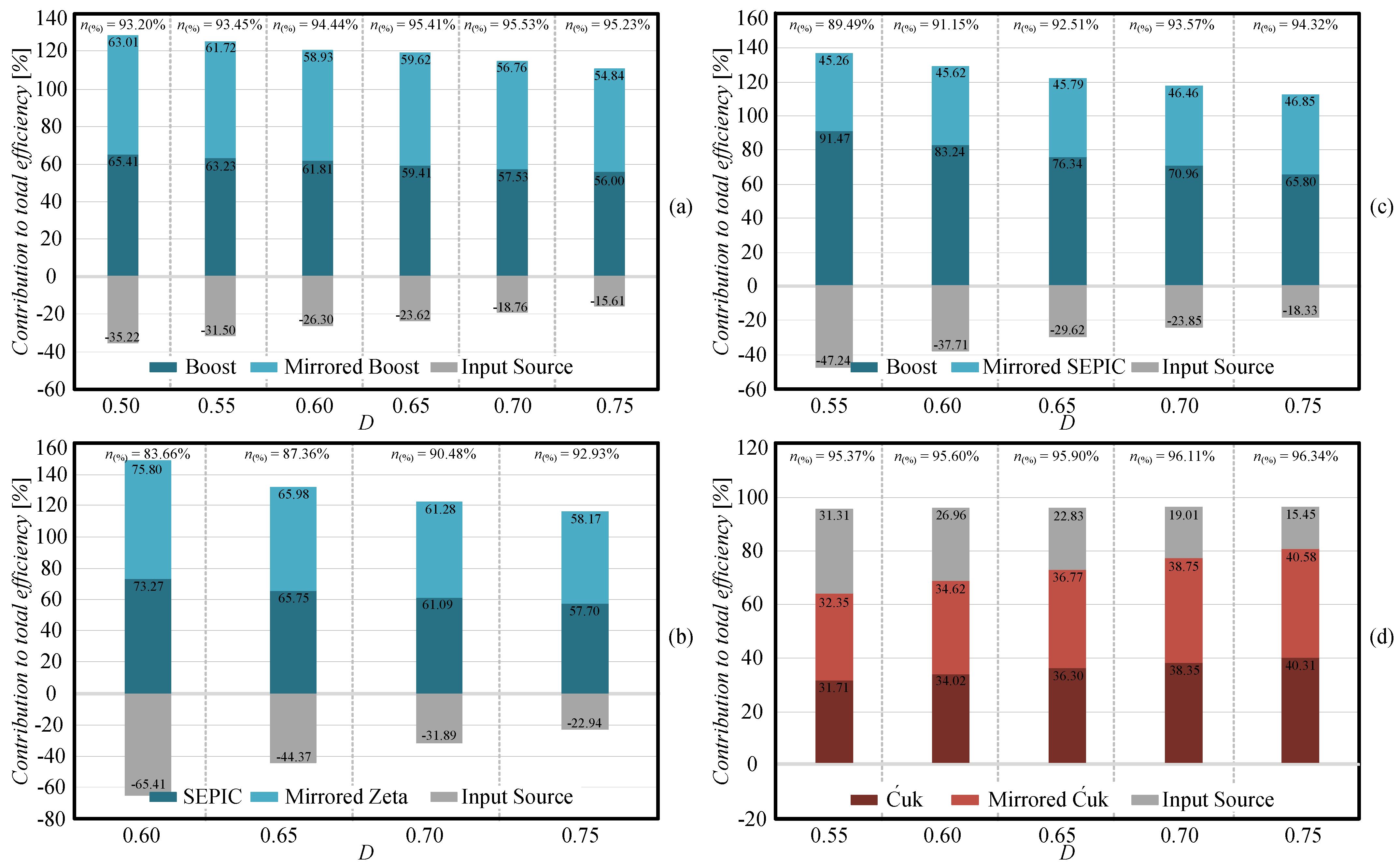
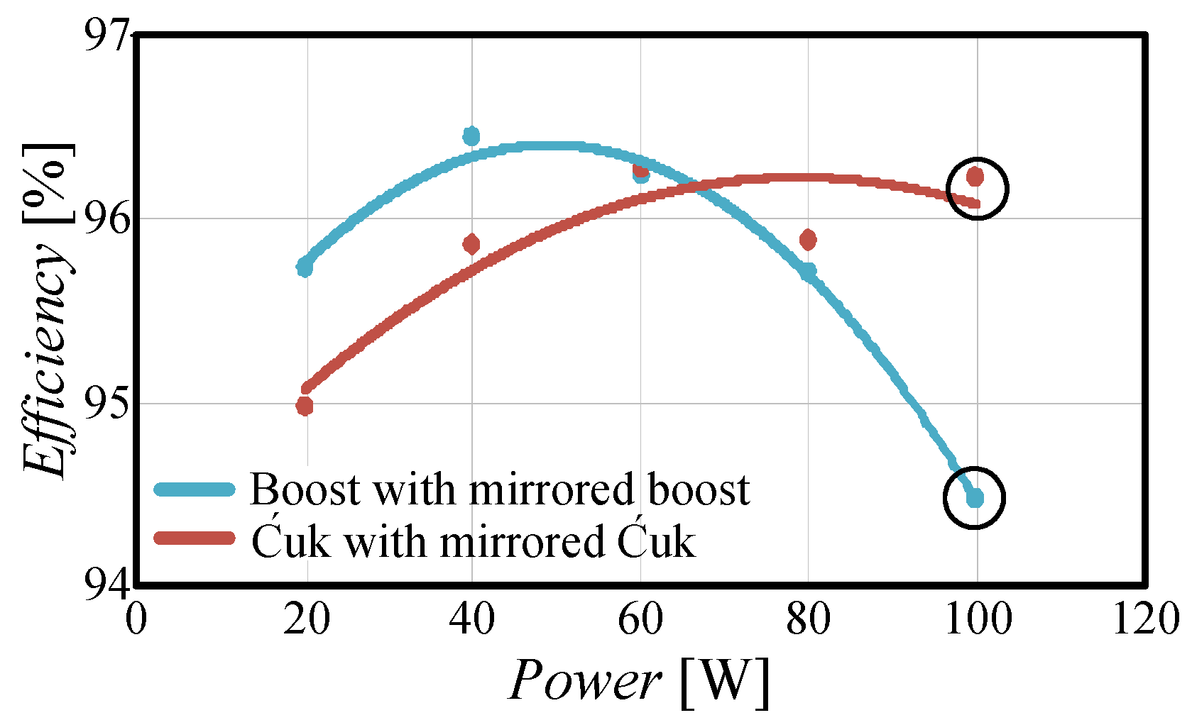
4. Experimental Results

In order to verify the theoretical analysis, ten prototypes (boost, SEPIC, zeta, Ćuk, buck-boost, and their mirrored versions) were assembled, as shown in Figure 9a, for the positive group, and in Figure 9b for the negative group. The specifications and components of the prototypes are exhibited in Table 2.
Figure 10 shows the results related to the connection between the boost and the mirrored boost converter. Figure 10a presents the input voltage (≈20 V), the output voltages of Converters 1 and 2 (≈80 V each), and the differential output voltage (≈140 V). The voltages values are in accordance with the equations of the first line of Table 1 and the output voltage follow Equation (2). The current waveforms are exhibited in Figure 10b. The waveform shown in the math channel (M3) proves Equation (8) (iin = iin1+iin2io), since the input current of both the converters are the same (iin1iin2 ≈ 2.9 A), and the input current (iin) is around 5 A and the output current (io) is approximately 784 mA.
Experimental results for the differential connection between the boost and the mirrored SEPIC converters with the same duty cycle (D = D1 = D2 = 0.75) are shown in Figure 11, and with different duty cycle (D1 = 0.7142 and D2 = 0.777) in Figure 12. The output voltage (Vo) is the same in both cases, however, the partial voltages (Vo1 and Vo2) are different [Figure 11a and Figure 12a]. In the first case (D1 = D2) Vo1 is around 80 V and Vo2 is 60 V, whereas in the second case (D1D2) Vo1 and Vo2 are 70 V. This last condition ensures that the converters process the same power. The voltages when D1 = D2 follow the equations present in the second line of Table 1 and when D1D2 follow the Equations (20) and (21). In both cases, the output voltage is given by Equation (2). The input currents of each of the basic converters in the first case (Figure 11b) are different (iin1 ≈ 3.35 A and iin2 ≈ 2.57 A), and in the second case (Figure 12b) are the same (iin1iin2 ≈ 2.9 A). It means that the duty cycles can be adjusted to balance the power processed by each converter, as detailed in Section 3.
The input and output currents considering other configurations for D1 = D2 are presented in Figure 13. Figure 13a refers to the connection between the SEPIC and the mirrored boost converters and Figure 13b between the Zeta and the mirrored boost converters. The voltages values are in accordance with the third line of Table 1. It should be noted that in these connections the converters process different amounts of power, which validates the theoretical analysis approached in Section 3. In order to ensure the power balance between the associated converters, their duty cycles should be adjusted to be different, and the expected results are similar to those presented in Figure 12.
The experimental results for the differential connection between the SEPIC and the mirrored SEPIC converters are shown in Figure 14. Figure 14a presents the input voltage (≈20 V), the output voltage of the Converters 1 and 2 (≈60 V), and differential output voltage (≈100 V). these voltage values follow the fourth line of Table 1. The current waveforms are exhibited in Figure 14b. Note that the input current of the basic converters are the same (iin1iin2 ≈ 3 A), which ensures they process the same power level. The average input current (iin) is around only 5 A and the output current (io) is approximately 1 A. The results shown in the math channel (M3) experimentally prove Equation (8) (iin = iin1+iin2io).
The current waveforms related to the differential connection between the SEPIC and the mirrored Zeta converters and between the Zeta and the mirrored SEPIC converters are presented in Figure 15a,b, respectively. In both cases, the power processed by each converter is the same, as described in Table 1.
Figure 16 shows the experimental results for the differential connection between the Ćuk and the mirrored Ćuk converters considering D = D1 = D2. The input voltage (≈ 20 V), the output voltages of Converters 1 and 2 (≈ 60 V), and differential output voltage (≈ 140 V) are shown in Figure 16a and are in accordance with the line fifth of Table 1. The input current (iin) is around 5 A, the input currents of both the converters are the same (iin1iin2 ≈ 2.16 A) and the output current is 727 mA, which proves (11). The sum of the current of each basic converter (iin1 + iin2 ≈ 4.32) A is lower than the input current (5 A), enforcing the idea that the input source delivers a parcel of the output power directly to the load.
Figure 17a,b presents the current waveforms for the differential connection between the Ćuk and the mirrored buck-boost and between the buck-boost and the mirrored Ćuk converters. As is the case in Figure 16, the input source delivers a parcel of output power directly to the load.

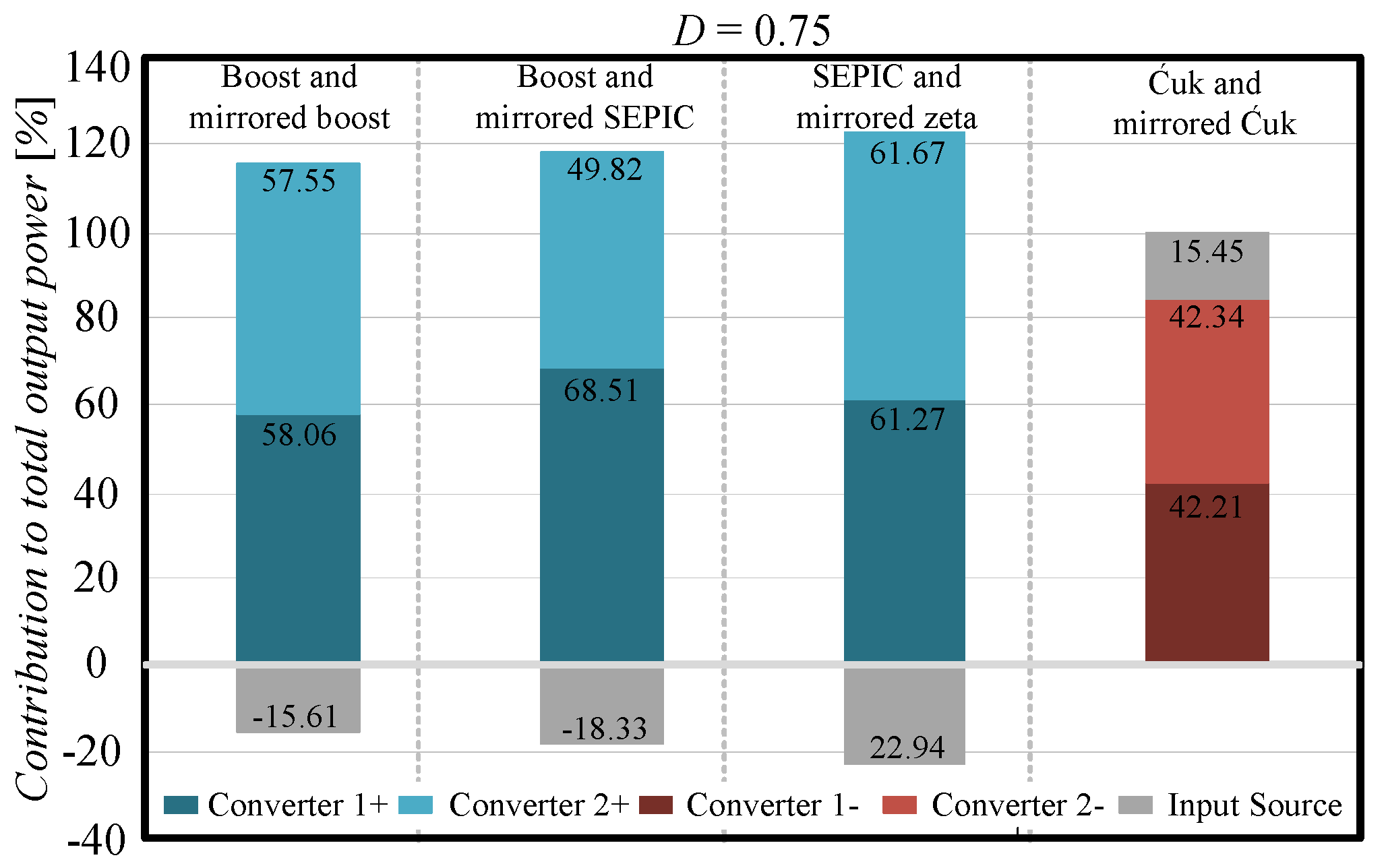
Power and Efficiency Analysis

The experimental percentage of power processed by each basic converter that composes the differential converter is exposed in Table 3 and exhibited in Figure 18, considering D = D1 = D2 = 0.75, and rated power equal to 100 W. The constructive parameters can affect the power processed by each element, however, the difference between the experimental values and the theoretical values are small and do not destabilize the converters or invalidate the developed methodology. The values of Table 3 are similar to the theoretical analysis present in Section 3 and Table 1. As one can note, in the positive group the input source decreases the total output power, whereas in the negative group it increases the output power. The theoretical and experimental behavior of the power processed in the differential converter for other duty cycle values is shown in Figure 5 and Figure 8.
Additionally, Table 3 depicts the efficiency comparison between the theoretical values obtained by Equations (24) and (25) and the experimental results. The source efficiency (nsource(%)) is herein assumed as 100% (ideal), that is, the parcel of power directly transferred from the input source to the load is free of losses. In all the evaluated cases, the error between the theoretical values and measurements is less than 0.15%, which proves the derived equation in practice.
The contribution of the Converter 1, Converter 2 and input source in relation to total output power and efficiency is presented in Figure 19, considering Vin = 20 V, Po = 100 W and different duty cycles values. Figure 19a,b, and c represent the converters of the positive group (boost and mirrored boost converters, boost and mirrored SEPIC converters, and SEPIC and mirrored Zeta converters, respectively).
The converters of the negative group are seen in Figure 19d (Ćuk and mirrored Ćuk converters). For the positive group, the input source contributes to decreasing the efficiency, and for the negative group it contributes to increasing the efficiency. In both groups, the influence of the input source on the efficiency decreases when the duty cycle increases. The experimental results shown in Table 3 also demonstrate that the negative group converters present higher efficiency when compared to the positive group converters. It occurs because the negative group converters operate as conventional 3P since the input source provides active power directly to the load.
Figure 20 shows the experimental efficiency curves in the function of output power for the boost with mirrored boost (positive group) and Ćuk with mirrored Ćuk (negative group). Both efficiency curves are higher than 95% at all output power ranges are analyzed. It should be highlighted that, even with a larger number of components, the Ćuk converter presents a higher efficiency in higher loads due to the power directly transferred by the 3P in negative groups.
Figure 21 shows the theoretical distribution of losses per component when the output power is 100 W (highlighted points in Figure 20) for the boost with a mirrored boost converter (Figure 21a) and for the Ćuk with mirrored Ćuk (Figure 21b). For both converters, the component responsible for the greatest parcel of losses is the inductor.

5. Conclusions

The paper has analyzed two types of differential converters based on the connection between basic converters of the same group, in order to evaluate their ability in realizing partial power processing. It was verified that differential converters of the positive group are featured by the circulation of non-active power since the sum of the power processed by each basic converter is higher than the power delivered to the load. This non-active power is lower as higher is the operating duty cycles, thus the use of converters of the positive group in differential connections are recommended only for high gain applications.
For differential converters of the negative group, the input source contributes positively with the differential voltage, thus the sum of the power processed by each basic converter is lower than the power delivered to the load, increasing the global efficiency. Thus, the use of differential converters of the negative group is recommended for any application that requires step-up converters. In fact, experimental results allow us to conclude that the differential converters of the negative group showed better efficiency when compared to those of the positive group for the analyzed operating points (D = 0.55 until 0.75).
Finally, it is important to highlight that differential connections may also be applied to integrated converters that use other lift voltage techniques, resulting in topologies able to ensure ultra-high gain and 3P to be applied simultaneously, in, for example, solar, wind, and storage systems.

Author Contributions

Conceptualization, J.M.d.A., R.F.C. and T.B.L.; methodology, J.M.d.A., R.F.C. and T.B.L.; validation, J.M.d.A.; formal analysis, J.M.d.A.; writing—original draft preparation, J.M.d.A., R.F.C. and T.B.L.; writing—review and editing, J.M.d.A., R.F.C. and T.B.L.; supervision, R.F.C. and T.B.L. All authors have read and agreed to the published version of the manuscript.

Funding

National Council for Scientific and Technological Development—Process n°. 141513/2018-7.

Informed Consent Statement

Not applicable.

Conflicts of Interest

The authors declare no conflict of interest.

References

  1. Sanjari, M.J.; Gooi, H.B.; Nair, N.C. Power Generation Forecast of Hybrid PV–Wind System. IEEE Trans. Sustain. Energy 2019, 11, 703–712. [Google Scholar] [CrossRef]
  2. Ku, T.T.; Lin, C.H.; Hsu, C.T.; Chen, C.S.; Liao, Z.Y.; Wang, S.D.; Chen, F.F. Enhancement of power system operation by renewable ancillary service. IEEE Trans. Ind. Appl. 2020, 56, 6150–6157. [Google Scholar] [CrossRef]
  3. Jia, K.; Yang, Z.; Fang, Y.; Bi, T.; Sumner, M.; Zhe, Y. Influence of inverter-interfaced renewable energy generators on directional relay and an improved scheme. IEEE Trans. Power Electron. 2019, 34, 11843–11855. [Google Scholar] [CrossRef]
  4. Hasanpour, S.; Siwakoti, Y.P.; Mostaan, A.; Blaabjerg, F. New semiquadratic high step-up dc/dc converter for renewable energy applications. IEEE Trans. Power Electron. 2021, 36, 433–446. [Google Scholar] [CrossRef]
  5. Saadatizadeh, Z.; Heris, P.C.; Sabahi, M.; Babaei, E. A dc–dc transformerless high voltage gain converter with low voltage stresses on switches and diodes. IEEE Trans. Power Electron. 2019, 34, 10600–10609. [Google Scholar] [CrossRef]
  6. Marzang, V.; Hosseini, S.H.; Rostami, N.; Alavi, P.; Mohseni, P.; Hashemzadeh, S.M. A high step-up nonisolated dc–dc converter with flexible voltage gain. IEEE Trans. Power Electron. 2020, 35, 10489–10500. [Google Scholar] [CrossRef]
  7. Cao, Y.; Samavatian, V.; Kaskani, K.; Eshraghi, H. A novel nonisolated ultra-high-voltage-gain dc–dc converter with low voltage stress. IEEE Trans. Ind. Electron. 2017, 64, 2809–2819. [Google Scholar] [CrossRef]
  8. Faridpak, B.; Bayat, M.; Nasiri, M.; Samanbakhsh, R.; Farrokhifar, M. Improved hybrid switched inductor/switched capacitor dc–dc converters. IEEE Trans. Power Electron. 2021, 36, 3053–3062. [Google Scholar] [CrossRef]
  9. Forouzesh, M.; Siwakoti, Y.P.; Gorji, S.A.; Blaabjerg, F.; Lehman, B. Step-up dc–dc converters: A comprehensive review of voltage-boosting techniques, topologies, and applications. IEEE Trans. Power Electron. 2017, 32, 9143–9178. [Google Scholar] [CrossRef]
  10. de Andrade, J.M.; Coelho, R.F.; Lazzarin, T.B. High step-up dc–dc converter based on modified active switched-inductor and switched-capacitor cells. IET Power Electron. 2020, 13, 3127–3137. [Google Scholar] [CrossRef]
  11. Salvador, M.A.; De Andrade, J.M.; Lazzarin, T.B.; Coelho, R.F. Nonisolated high-step-up dc–dc converter derived from switched-inductors and switched-capacitors. IEEE Trans. Ind. Electron. 2020, 67, 8506–8516. [Google Scholar] [CrossRef]
  12. Salvador, M.A.; Lazzarin, T.B.; Coelho, R. High step-up dc–dc converter with active switched-inductor and passive switched-capacitor networks. IEEE Trans. Ind. Electron. 2018, 65, 5644–5654. [Google Scholar] [CrossRef]
  13. Kumar, G.G.; Sundaramoorthy, K.; Karthikeyan, V.; Babaei, E. Switched capacitor–inductor network based ultra-gain dc–dc converter using single switch. IEEE Trans. Ind. Electron. 2020, 67, 10274–10283. [Google Scholar] [CrossRef]
  14. Zhang, X.; Sun, L.; Guan, Y.; Han, S.; Cai, H.; Wang, Y.; Xu, D.G. Novel high step-up soft-switching dc–dc converter based on switched capacitor and coupled inductor. IEEE Trans. Power Electron. 2020, 35, 9471–9481. [Google Scholar] [CrossRef]
  15. Azizkandi, M.E.; Sedaghati, F.; Shayeghi, H.; Blaabjerg, F. A high voltage gain dc–dc converter based on three winding coupled inductor and voltage multiplier cell. IEEE Trans. Power Electron. 2020, 35, 4558–4567. [Google Scholar] [CrossRef]
  16. Mirzaee, A.; Moghani, J.S. Coupled inductor-based high voltage gain dc–dc converter for renewable energy applications. IEEE Trans. Power Electron. 2020, 35, 7045–7057. [Google Scholar] [CrossRef]
  17. Majeed, Y.E.; Ahmad, I.; Habibi, D. A multiple-input cascaded dc–dc converter for very small wind turbines. IEEE Trans. Ind. Electron. 2019, 66, 4414–4423. [Google Scholar] [CrossRef]
  18. Lee, S.-W.; Do, H.-L. High step-up coupled-inductor cascade boost dc–dc converter with lossless passive snubber. IEEE Trans. Ind. Electron. 2018, 65, 7753–7761. [Google Scholar] [CrossRef]
  19. de Andrade, J.M.; Salvador, M.A.; Coelho, R.F.; Lazzarin, T.B. General method for synthesizing high gain step-up dc–dc converters based on differential connections. IEEE Trans. Power Electron. 2020, 35, 13239–13254. [Google Scholar] [CrossRef]
  20. Salvador, M.A.; de Andrade, J.M.; Coelho, R.F.; Lazzarin, T.B. Methodology for synthesis of high-gain step-up dc–dc converters based on differential connections. Int. J. Circuit Theory Appl. 2020, 49, 306–326. [Google Scholar] [CrossRef]
  21. Caceres, R.O.; Barbi, I. A boost dc–ac converter: Analysis, design, and experimentation. IEEE Trans. Power Electron. 1999, 14, 134–141. [Google Scholar] [CrossRef]
  22. de Andrade, J.M.; Coelho, R.F.; Lazzarin, T.B. New high step-up dc-dc converter with quasi-z-source network and switched-capacitor cell. In Proceedings of the IEEE Applied Power Electronics Conference and Exposition (APEC), New Orleans, LA, USA, 14–17 June 2020; pp. 2062–2066. [Google Scholar]
  23. de Andrade, J.M.; Coelho, R.F.; Lazzarin, T.B. High step-up dc-dc converter based on the differential connection of basic converters and switched-capacitor cells. Int. J. Circuit Theory Appl. 2021, 49, 2555–2577. [Google Scholar] [CrossRef]
  24. Zientarski, J.R.R.; Martins, M.L.D.S.; Pinheiro, J.R.; Hey, H.L. Evaluation of power processing in series-connected partial-power converters. IEEE J. Emerg. Sel. Top. Power Electron. 2019, 7, 343–352. [Google Scholar] [CrossRef]
  25. Zientarski, J.R.R.; Martins, M.L.d.S.; Pinheiro, J.R.; Hey, H.L. Series-connected partial-power converters applied to pv systems: A design approach based on step-up/down voltage regulation range. IEEE Trans. Power Electron. 2018, 33, 7622–7633. [Google Scholar] [CrossRef]
  26. Choi, S.; Agelidis, V.; Yang, J.; Coutellier, D.; Marabeas, P. Analysis, design and experimental results of a floating-output interleaved-input boost-derived dc–dc high-gain transformer-less converter. IET Power Electron. 2011, 4, 168–180. [Google Scholar] [CrossRef]
  27. Coutellier, D.; Agelidis, V.G.; Choi, S. Experimental verification of floating-output interleaved-input dc-dc high-gain transformer-less converter topologies. In Proceedings of the IEEE Power Electronics Specialists Conference, Rhodes, Greece, 15–19 June 2008; pp. 562–568. [Google Scholar]
  28. Garcia, F.S.; Pomilio, J.A.; Spiazzi, G. Modeling and control design of the interleaved double dual boost converter. IEEE Trans. Ind. Electron. 2013, 60, 3283–3290. [Google Scholar] [CrossRef]
  29. Reddy, K.J.; Sudhakar, N. High voltage gain interleaved boost converter with neural network based MPPT controller for fuel cell based electric vehicle applications. IEEE Access 2018, 6, 3899–3908. [Google Scholar] [CrossRef]
Figure 1. Differential connections between two basic converters of different groups-boost converter connected with a buck-boost converter.
Energies 15 01159 g001
Figure 2. Differential connection between two basic converters of the same group-boost converter connected with a mirrored boost converter.
Energies 15 01159 g002
Figure 3. Generalized view of differential connection between two basic converters of the same group: (a) positive group and (b) negative group.
Energies 15 01159 g003
Figure 4. Equivalent circuits related to the output voltage loop of differential converters: (a) positive group and (b) negative group.
Energies 15 01159 g004
Figure 5. Theoretical curves and experimental points considering D = D1 = D2 at Po = 100 W and Vin = 20 V for the positive group: (a) boost and mirrored boost converters (positive group); (b) boost and mirrored SEPIC converters (positive group); (c) SEPIC and mirrored Zeta converters (positive group); (d) Ćuk and mirrored Ćuk converters (negative group).
Energies 15 01159 g005
Figure 6. Differential converters of positive group: (a) boost with mirrored boost, (b) boost with mirrored SEPIC, (c) boost with mirrored zeta, (d) SEPIC with mirrored boost, (e) SEPIC with mirrored SEPIC, (f) SEPIC with mirrored zeta, (g) zeta with mirrored boost, (h) zeta with mirrored SEPIC and (i) zeta with mirrored zeta.
Energies 15 01159 g006
Figure 7. Differential converters of negative group: (a) buck-boost with mirrored buck-boost, (b) buck-boost with mirrored Ćuk, (c) Ćuk with mirrored Ćuk and (d) Ćuk with mirrored buck-boost.
Energies 15 01159 g007
Figure 8. Theoretical curves of the power processed by the boost and the mirrored SEPIC or Zeta converters in the differential connection considering D1D2. Experimental points acquired under Po = 100 W and Vin = 20 V for the connection between the boost and the mirrored SEPIC converters.
Energies 15 01159 g008
Figure 9. Prototypes of Converter 1 and 2: (a) positive group—boost, SEPIC and zeta converters. (b) negative group—Ćuk and buck-boost converters. Dimension: 65 mm × 65 mm × 49 mm—each buck-boost converter and the others have 65 mm × 65 mm × 35 mm each converter.
Energies 15 01159 g009
Figure 10. Experimental results with same duty cycle (D = D1 = D2): boost and mirrored boost converters. (a) input voltage (Vin), partial output voltages (Vo1 and Vo2), and differential output voltage (Vo); (b) input current (iin), input current of Converters 1 and 2 (iin1 and iin2), output current (io), and input current calculated by the math channel (iin = iin1+iin2io).
Energies 15 01159 g010
Figure 11. Experimental results for boost with mirrored SEPIC converters with same duty cycle (D = D1 = D2): (a) input voltage (Vin), partial output voltages (Vo1 and Vo2), and differential output voltage (Vo); (b) input current (iin), input current of Converters 1 and 2 (iin1 and iin2), output current (io), and input current calculated by the math channel (iin = iin1+iin2io).
Energies 15 01159 g011
Figure 12. Experimental results for boost with mirrored SEPIC converters with different duty cycle (D1D2): (a) input voltage (Vin), partial output voltages (Vo1 and Vo2), and differential output voltage (Vo); (b) input current (iin), input current of Converters 1 and 2 (iin1 and iin2), output current (io), and input current calculated by the math channel (iin = iin1+iin2io).
Energies 15 01159 g012
Figure 13. Experimental results with same duty cycle (D = D1 = D2): (a) SEPIC and mirrored boost converters and (b) Zeta and mirrored boost converters. Input current (iin), input current of Converters 1 and 2 (iin1 and iin2), output current (io), and input current calculated by the math channel (iin = iin1+iin2io).
Energies 15 01159 g013
Figure 14. Experimental results with the same duty cycle (D = D1 = D2): SEPIC and mirrored SEPIC converters. (a) input voltage (Vin), partial output voltages (Vo1 and Vo2), and differential output voltage (Vo); (b) input current (iin), input current of Converters 1 and 2 (iin1 and iin2), output current (io), and input current calculated by the math channel (iin = iin1+iin2io).
Energies 15 01159 g014
Figure 15. Experimental results with same duty cycle (D = D1 = D2): (a) SEPIC and mirrored Zeta converters; (b) Zeta and mirrored SEPIC converters. Input current (iin), input current of Converters 1 and 2 (iin1 and iin2), output current (io), and input current calculated by the math channel (iin = iin1+iin2io).
Energies 15 01159 g015
Figure 16. Experimental results with same duty cycle (D = D1 = D2): Ćuk and mirrored Ćuk converters. (a) input voltage (Vin), partial output voltages (Vo1 and Vo2), and differential output voltage (Vo); (b) input current (iin), input current of Converters 1 and 2 (iin1 and iin2), output current (io), and input current calculated by the math channel (iin = iin1+iin2io).
Energies 15 01159 g016
Figure 17. Experimental results with the same duty cycle (D = D1 = D2): (a) Ćuk and mirrored buck-boost converters; (b) buck-boost and mirrored Ćuk converters. Input current (iin), input current of Converters 1 and 2 (iin1 and iin2), output current (io), and input current calculated by the math channel (iin = iin1+iin2io).
Energies 15 01159 g017
Figure 18. Experimental results related to the distribution of the total output power among the converter 1, converter 2 and input source considering D = D1 = D2 = 0.75, Vin = 20 V and Po = 100 W.
Energies 15 01159 g018
Figure 19. Experimental Results considering D = D1 = D2 = 0.75, Vin = 20 V and Po = 100 W: (a) boost and mirrored boost converters; (b) SEPIC and mirrored Zeta converters; (c) boost and mirrored SEPIC converters, and (d) Ćuk and mirrored Ćuk converters.
Energies 15 01159 g019
Figure 20. Experimental efficiency curves in relation of output power for boost with mirrored boost and Ćuk with mirrored Ćuk.
Energies 15 01159 g020
Figure 21. Theoretical distribution of losses in 100 W: (a) boost with mirrored boost and (b) Ćuk with mirrored Ćuk.
Energies 15 01159 g021
Table 1. Power behavior in each basic converter of the differential converter considering D = D1 = D2.
Converter 1Converter 2GCCM1GCCM2GCCMP1(%)P2(%)Psource(%)
BoostMirrored Boost 1 1 D 1 1 D 1 + D 1 D 1 D + 1 1 D + 1 1 D D + 1
BoostMirrored SEPIC or Zeta 1 1 D D 1 D 2 D 1 D 1 2 D 1 2 1 D 2 D
SEPIC or ZetaMirrored Boost D 1 D 1 1 D 2 D 1 D 1 2 1 2 D 1 D 2 D
SEPIC or ZetaMirrored SEPIC or Zeta D 1 D D 1 D 3 D 1 1 D D 3 D 1 D 3 D 1 1 D 3 D 1
Ćuk or Buck-BoostMirrored Ćuk or Buck-Boost D 1 D D 1 D 1 + D 1 D D 1 + D D 1 + D 1 D 1 + D
Table 2. Design specifications and components employed in the prototype.
Input Voltage (Vin)20 V
Duty Cycle (D1)0.75
Power output (P1 and P2)100 W
Switching Frequency (fs)50 kHz
First inductor of boost, SEPIC, Zeta and Ćuk converters and the mirrored versions300 µH; Core: E30/14; Turns: 46; Wire: 3 × AWG22
Second inductor of SEPIC, Zeta and Ćuk converters and the mirrored versions900 µH; Core: E30/14; Turns: 55; Wire: 2 × AWG22
Inductor of Buck-Boost converter and mirrored version340 µH; Core: E42/15; Turns: 46; Wire: 4 × AWG22
Output Capacitors2 × 10 µF/100 V
Second capacitor of SEPIC, Zeta and Ćuk converters and the mirrored versions2 × 3.3 µF/100 V
SwitchesFDD86250; 150 V/50 A
DiodesTSP15H150; 150 V/15 A
Gate DriverHalf-Bridge + FOD3180
Digital Signal ProcessorTMS320F28069
Table 3. Percentage of the experimental output power processed by each basic converter and by the input source, and further efficiency comparison between theoretical and experimental values (Po = 100 W).
Converter 1Converter 2Experimental ValuesTheo. n(%)
Equations (20) and (21)
Error%
P1(%)P2(%)Psource(%)n1(%)n2(%)n(%)
D = D1 = D2
BoostMirrored Boost58.06%57.55%15.61%96.46%95.29%95.31%95.23%0.07%
BoostMirrored SEPIC68.51%49.82%18.33%96.05%94.03%94.40%94.32%0.08%
BoostMirrored Zeta67.24%49.83%17.08%96.57%94.50%94.88%94.96%0.08%
SEPICMirrored Boost49.93%67.24%17.17%93.92%95.51%94.05%93.94%0.11%
SEPICMirrored SEPIC60.50%59.85%20.35%93.77%93.25%92.17%92.19%0.02%
SEPICMirrored Zeta61.27%61.67%22.94%94.17%94.33%93.00%92.93%0.07%
ZetaMirrored Boost50.15%66.92%17.07%94.94%95.93%94.69%94.74%0.05%
ZetaMirrored SEPIC60.61%60.16%20.77%94.26%93.52%92.66%92.63%0.03%
ZetaMirrored Zeta60.66%59.68%20.35%94.63%93.71%92.98%92.98%0.00%
ĆukMirrored Ćuk42.21%42.34%15.45%95.51%95.83%96.37%96.34%0.02%
ĆukMirrored Buck-Boost43.05%42.46%14.49%95.39%94.31%95.52%95.60%0.08%
Buck-BoostMirrored Buck-Boost42.69%42.46%14.86%95.04%94.48%95.46%95.52%0.07%
Buck-BoostMirrored Ćuk42.61%42.88%14.51%95.11%95.37/595.90%95.93%0.03%
D1D2
BoostSEPIC60.17%57.53%17.70%96.66%93.60%94.33%94.310.01%
Publisher’s Note: MDPI stays neutral with regard to jurisdictional claims in published maps and institutional affiliations.

