
A Novel Single-Switch High Step-Up DC–DC Converter with Three-Winding Coupled Inductor

 ,
,  ,
,  ,
,  ,
,  and
and
Abstract
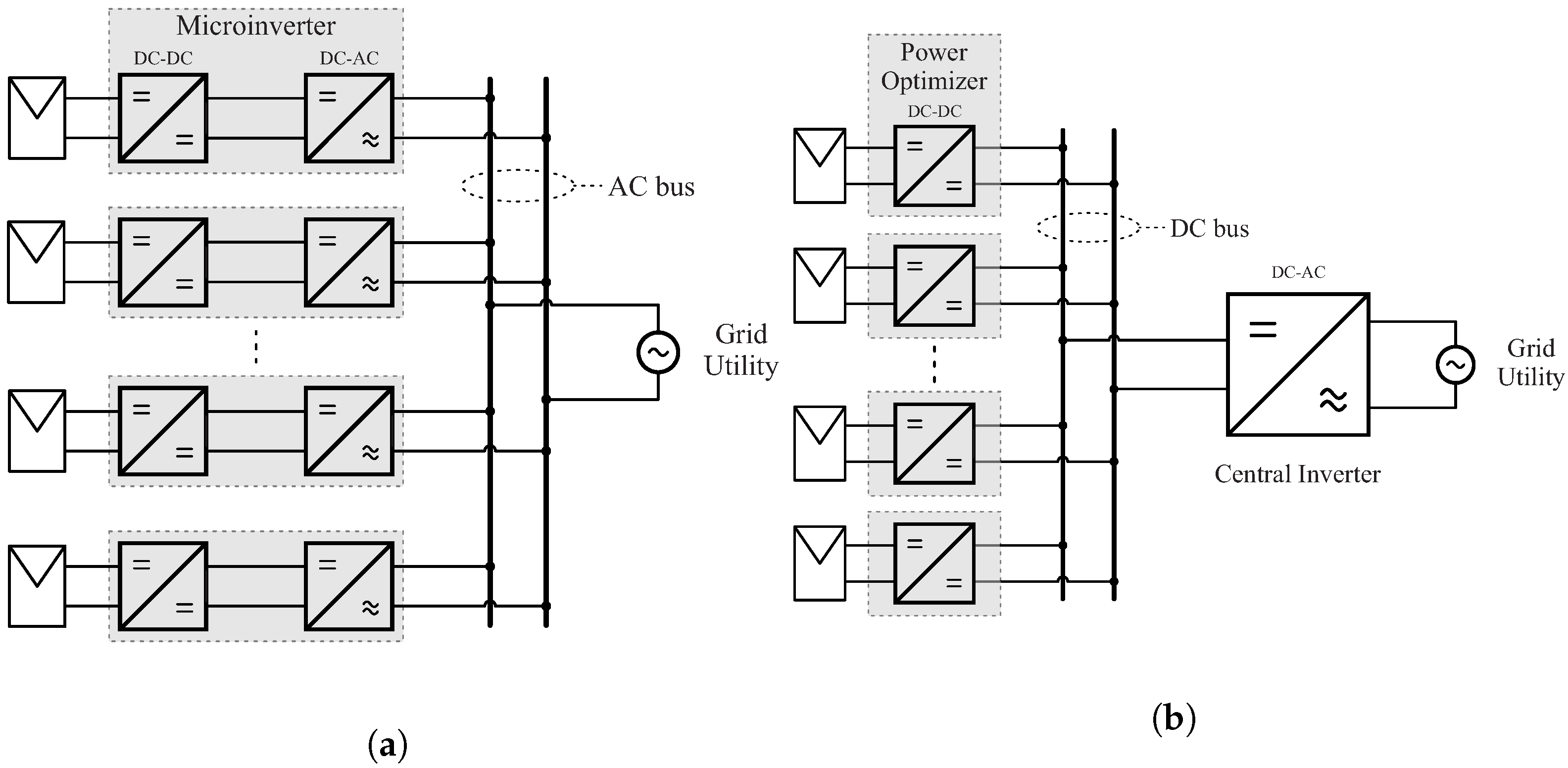
:1. Introduction
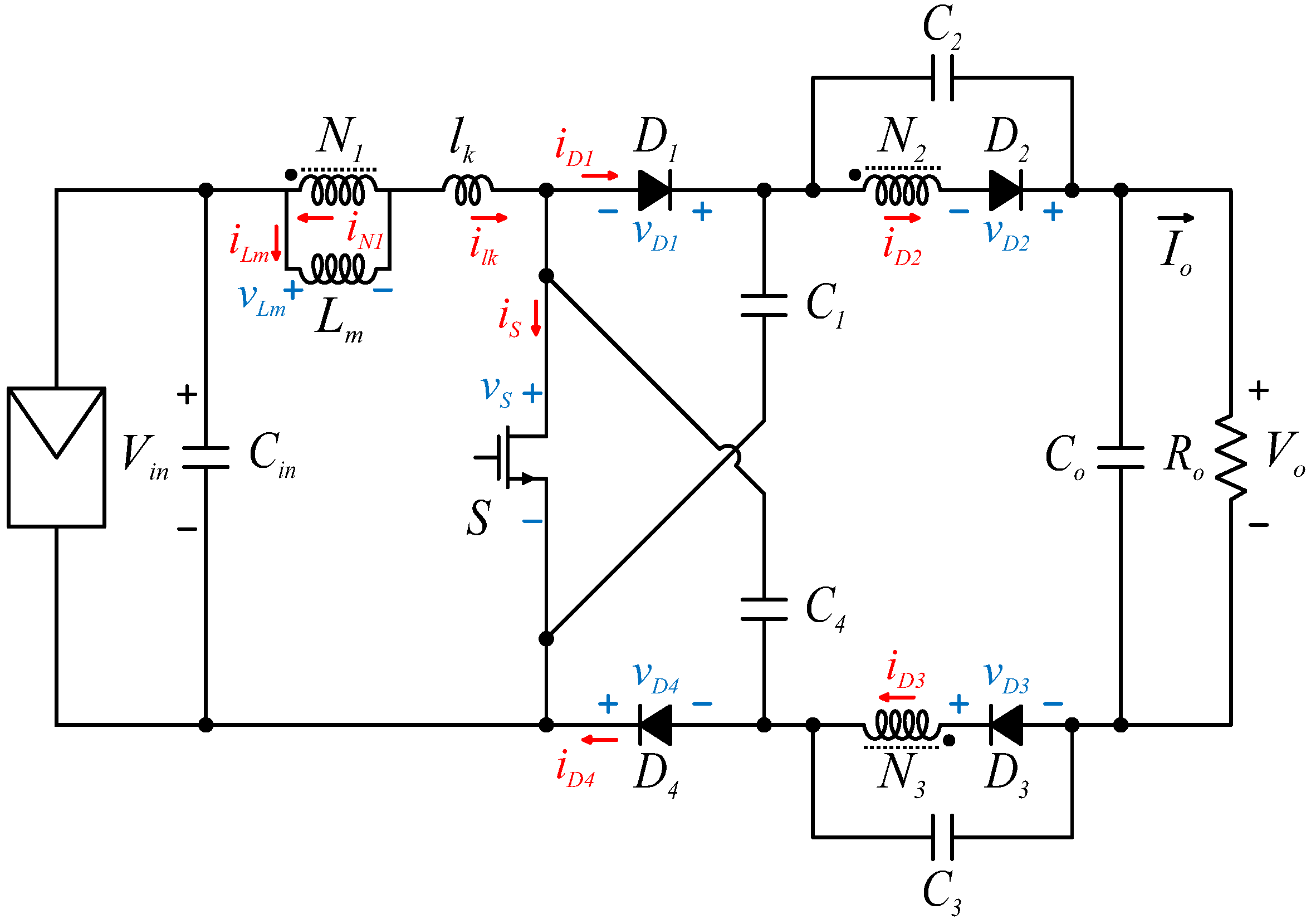
2. Operational Principle and Analysis
- , and are the primary and the two secondary turn numbers, respectively, in which ;
- is the leakage inductance of the coupled inductor;
- is the magnetizing inductance of the coupled inductor;
- S is the single switch;
- and are the clamper circuit diodes;
- and are the switched capacitors’ diodes;
- and are the clamper circuit capacitors;
- and are the switched capacitors;
- is the output capacitor;
- is the input capacitor.
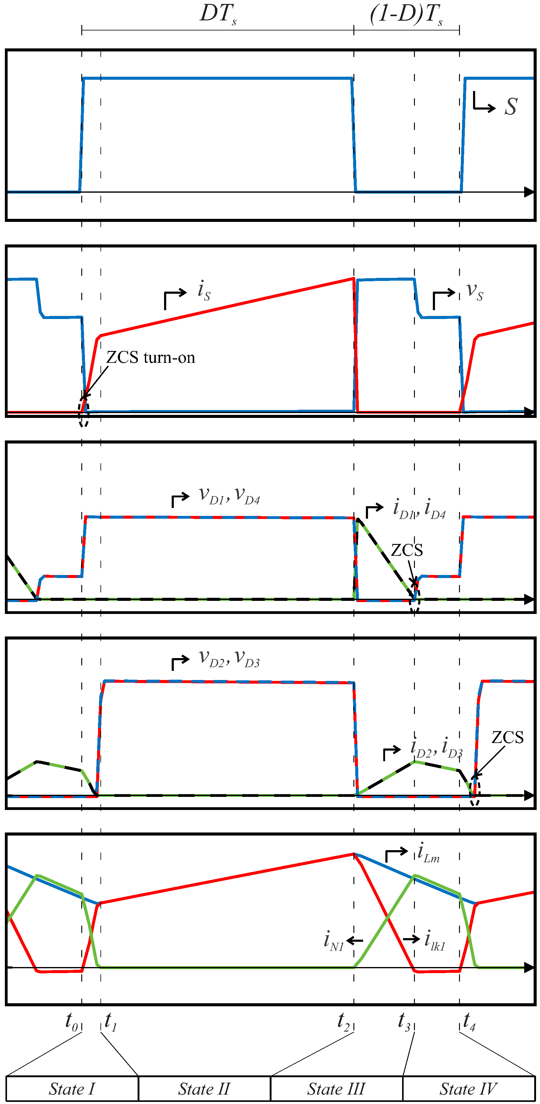
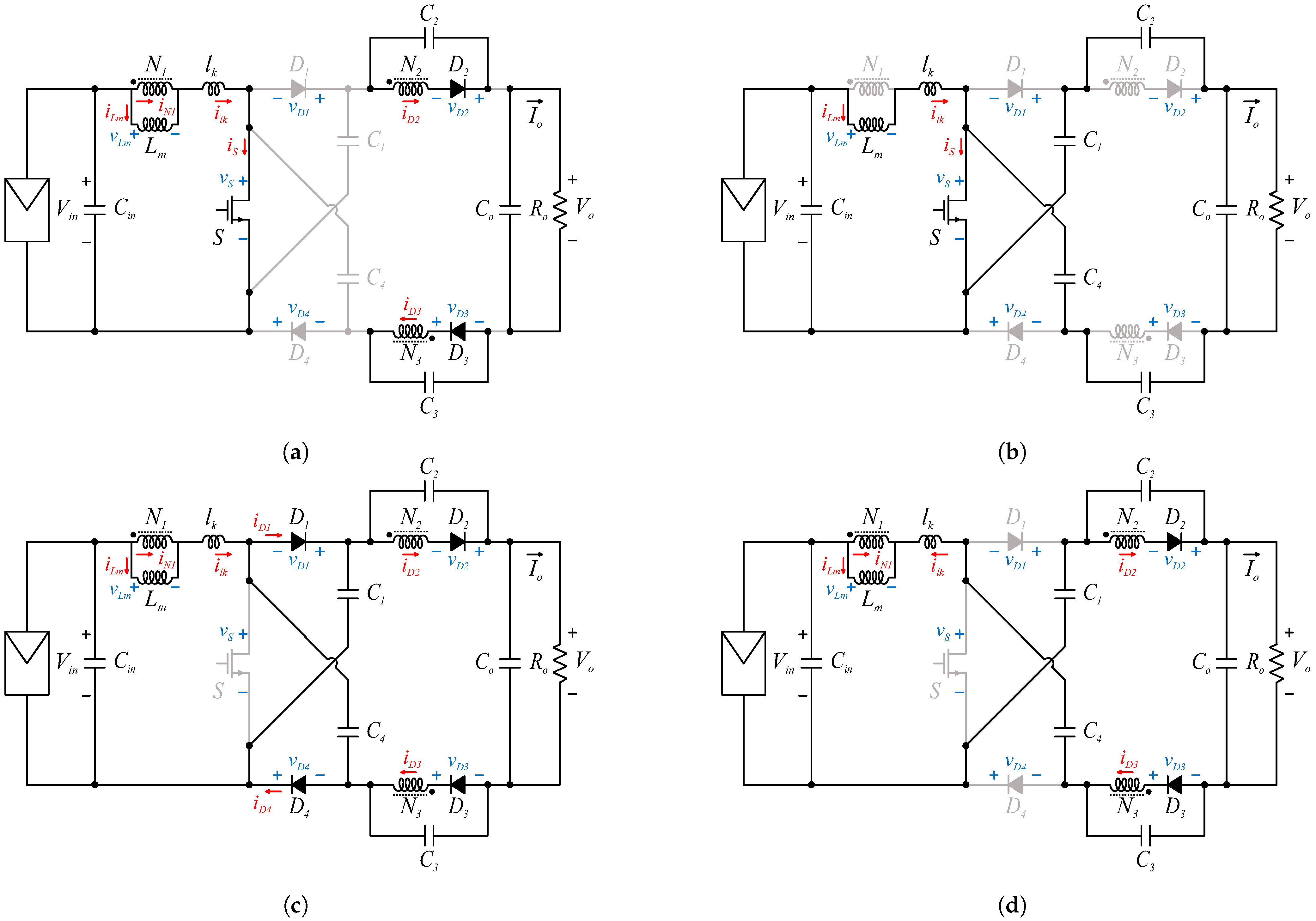
Operating States
3. Steady-State Analysis
- All components are ideal;
- ;
- The capacitance values of the switched capacitors are the same;
- The capacitance values of the clamper circuit capacitors are the same;
- Capacitors are large enough to reasonably neglect the voltage ripples.
3.1. Voltage Gain Derivation
3.2. Semiconductors’ Voltage Stress
3.3. Average Current Stresses
3.4. Maximum Current Stresses
4. Design Considerations
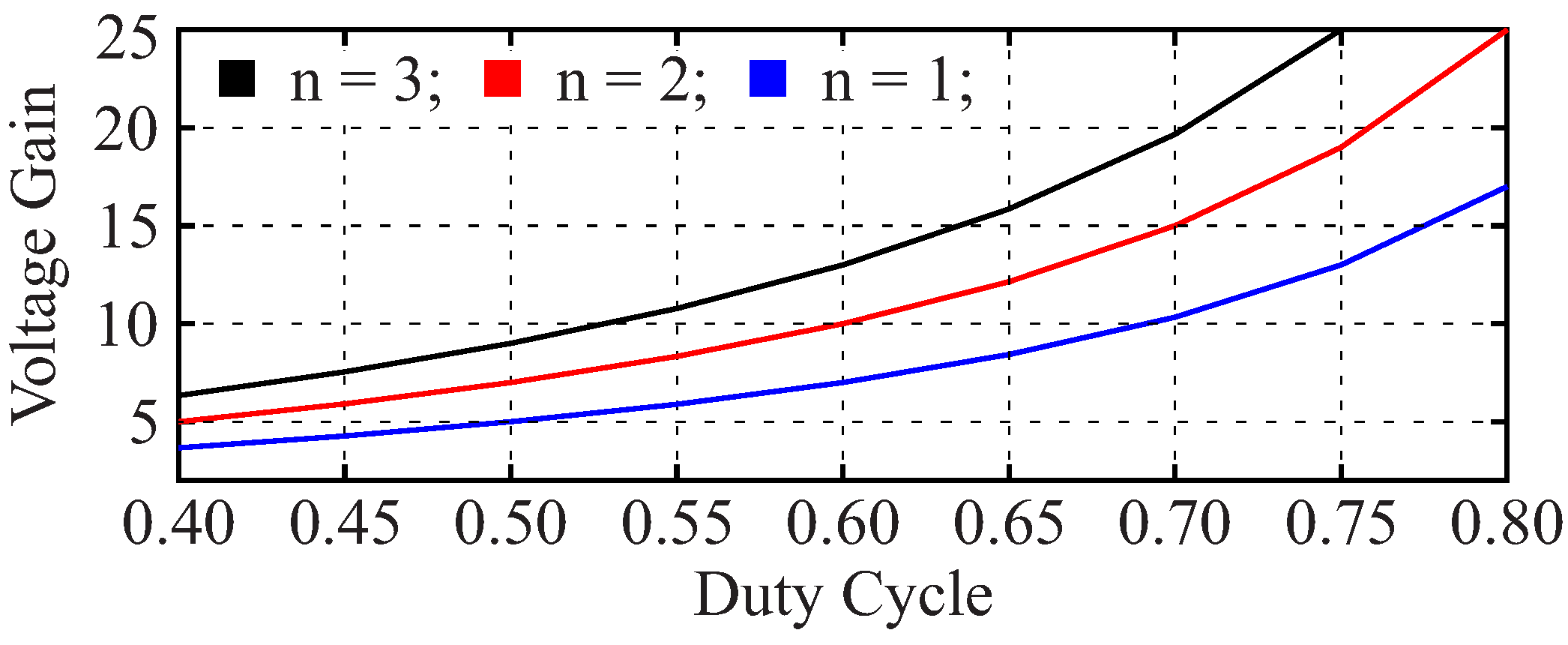
4.1. Turns Ratio Selection
4.2. Magnetizing Inductance Selection
4.3. Capacitance Selection
4.4. Semiconductor Devices Selection
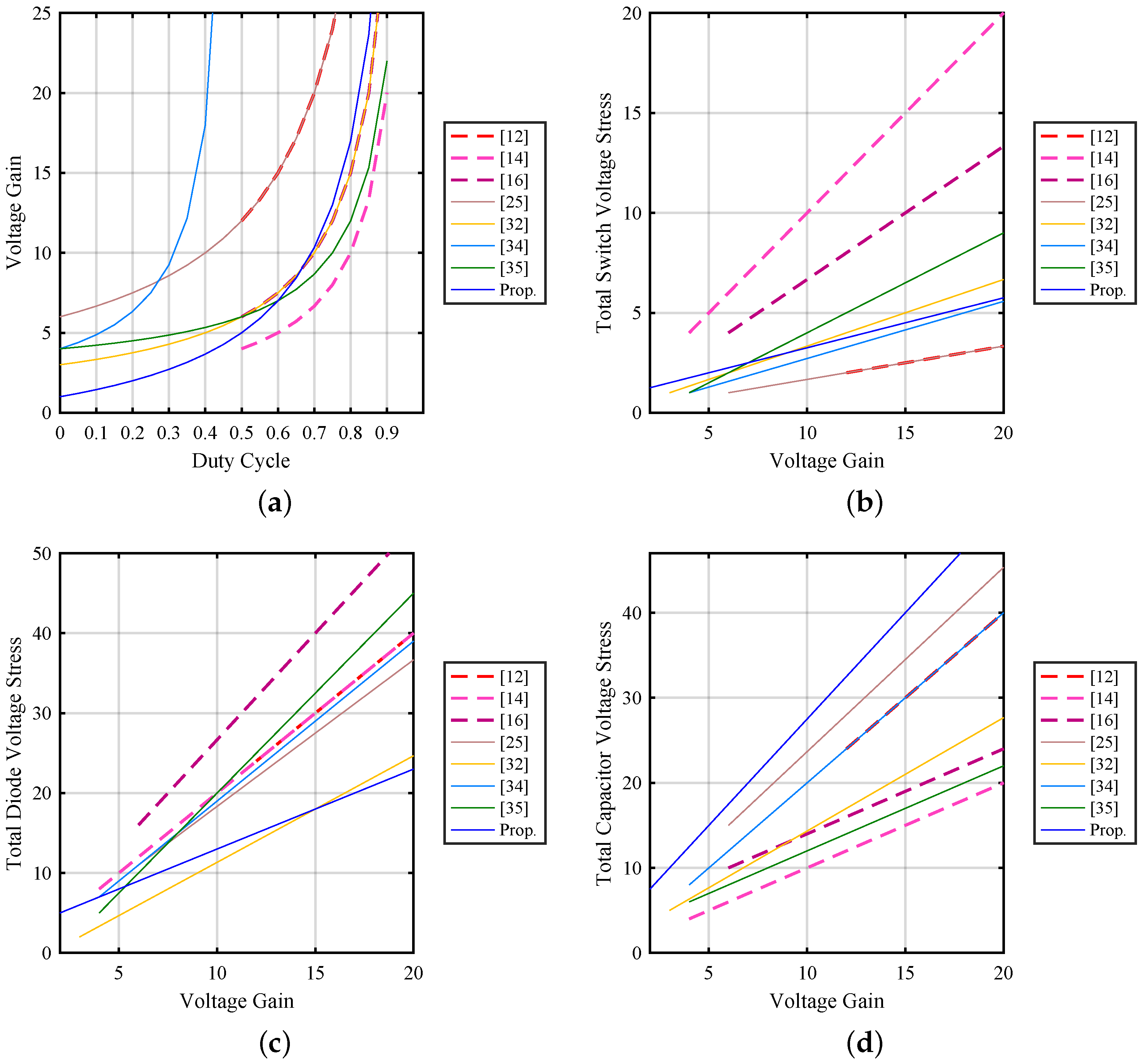
5. Performance Comparison
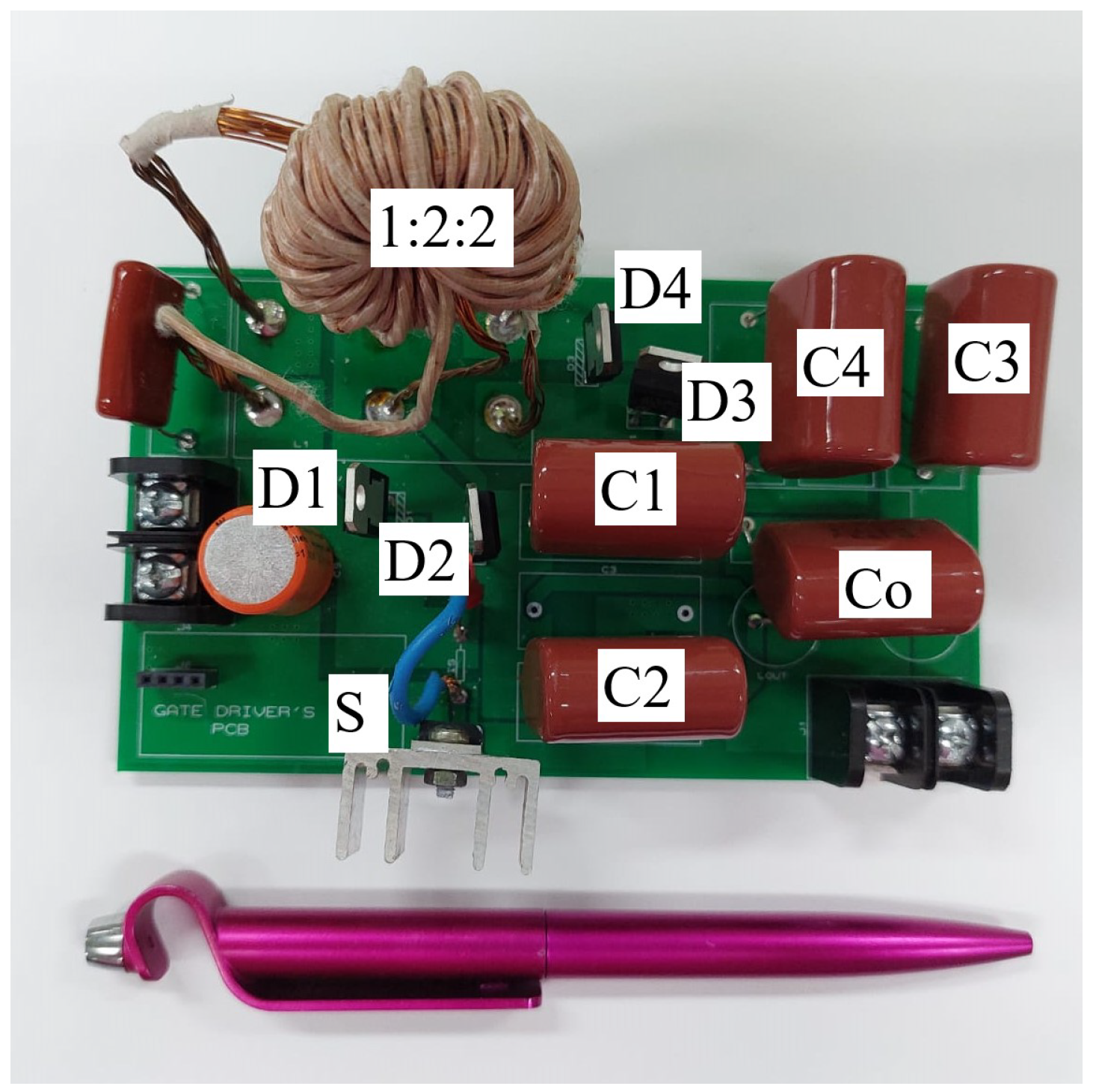
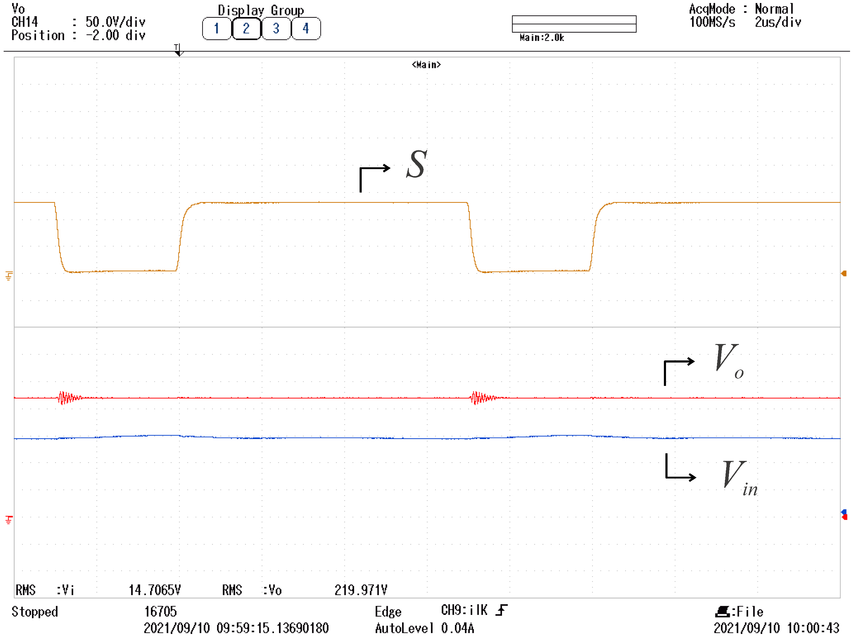
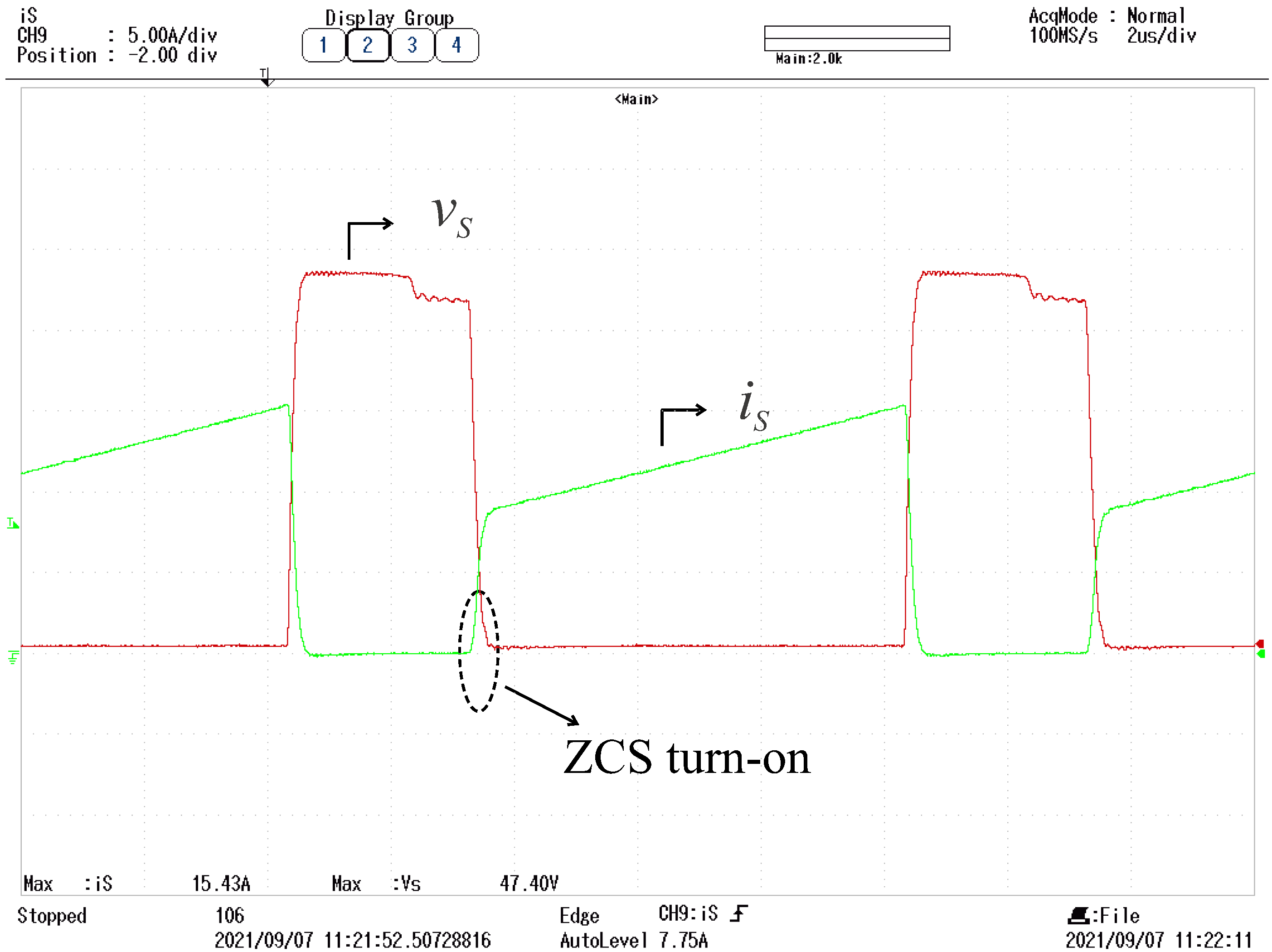
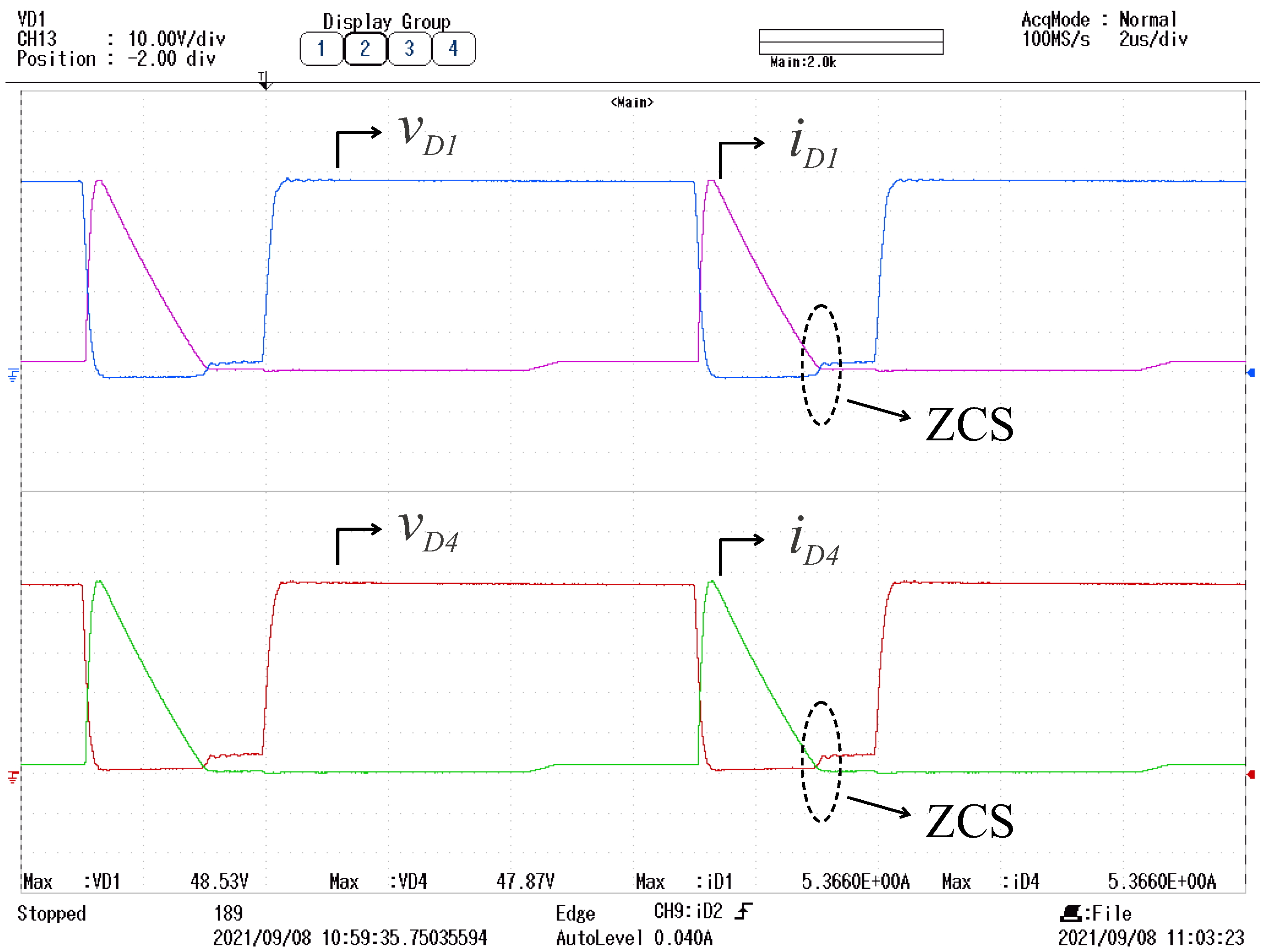
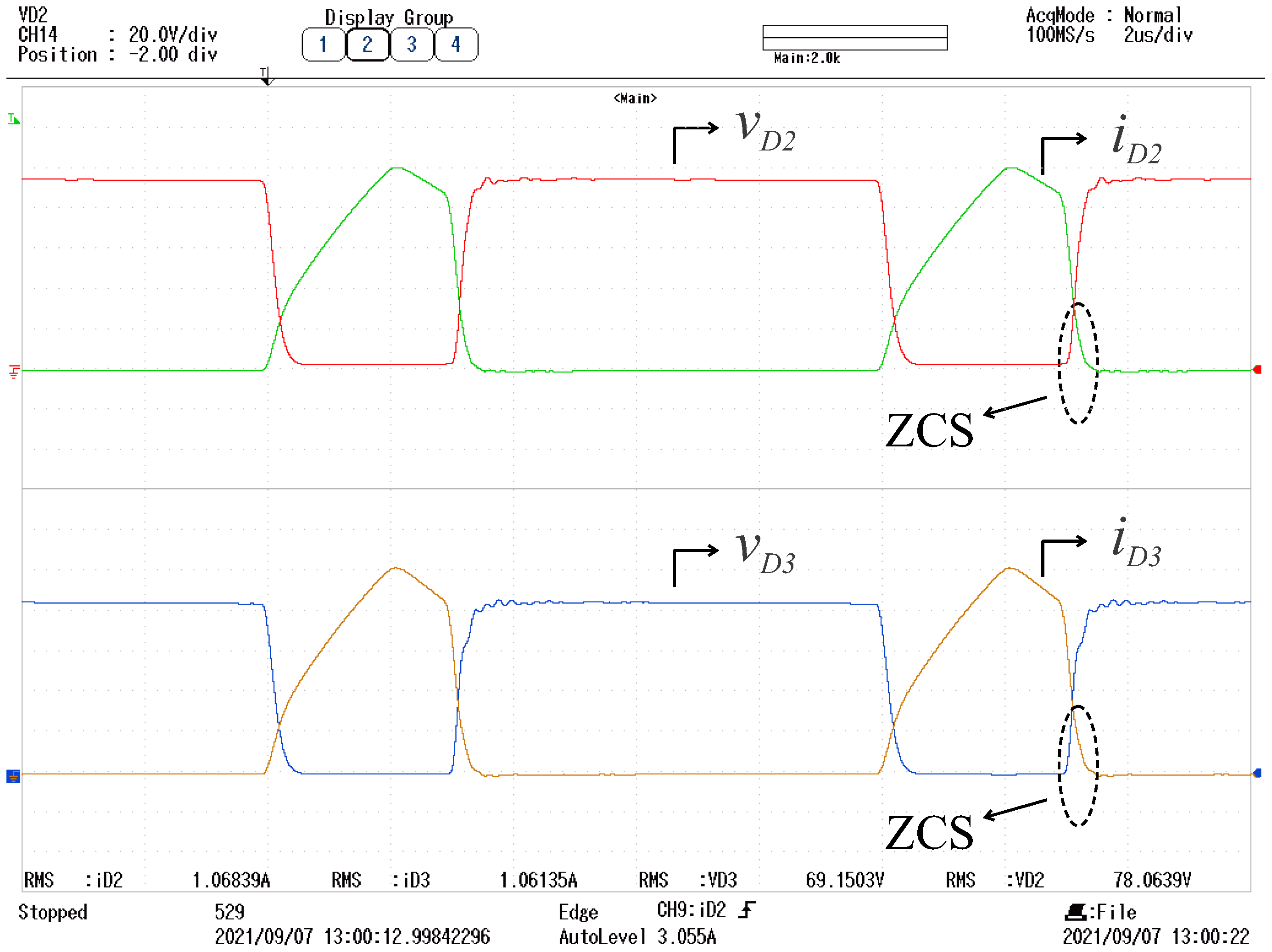
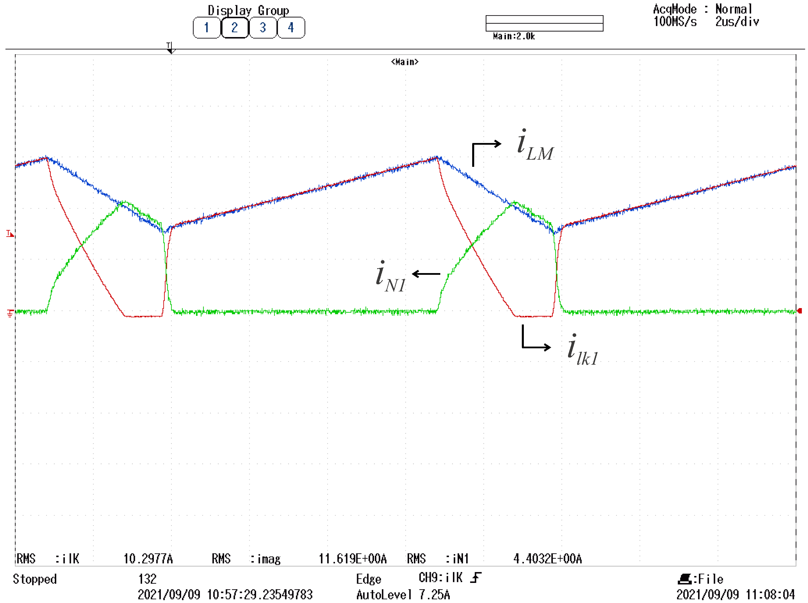
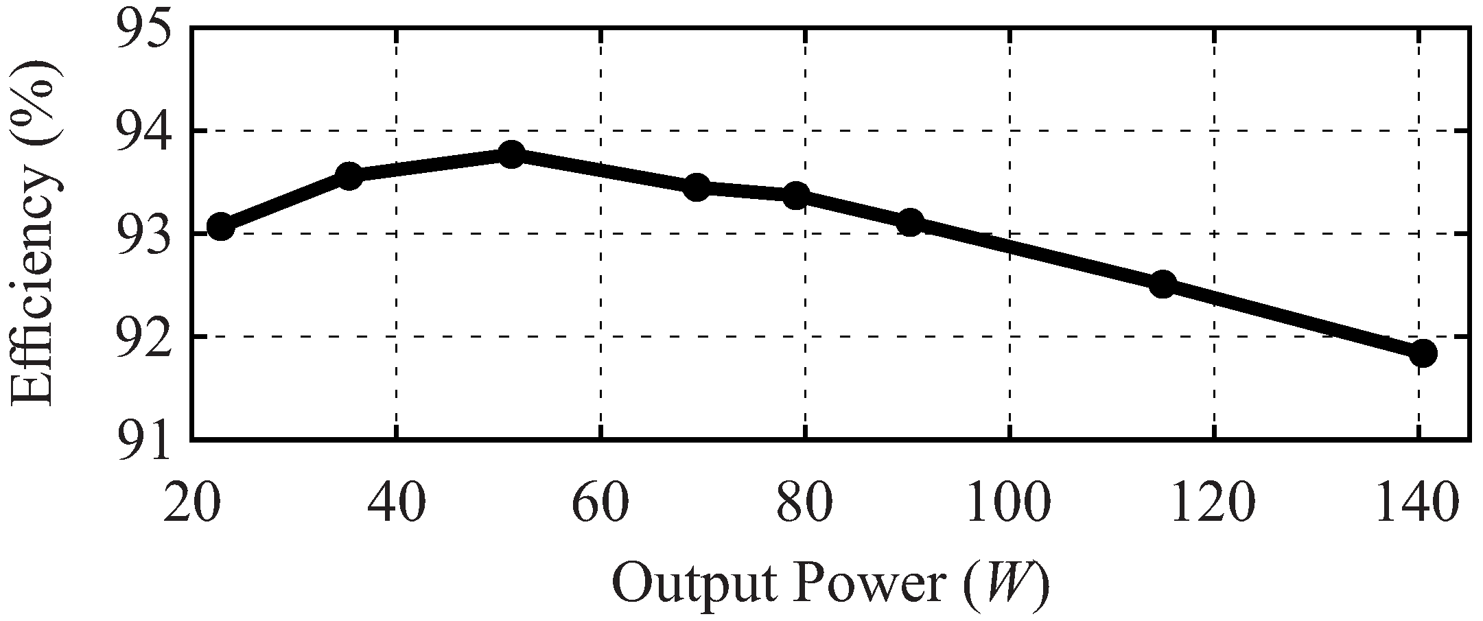
6. Experimental Results
7. Conclusions
Author Contributions
Funding
Acknowledgments
Conflicts of Interest
Abbreviations
| AC | Alternating current |
| CCM | Conntinuous Conduction Mode |
| DC | Direct current |
| ESR | Equivalent Series Resistance |
| IPOS | Input-parallel Output-series |
| MOSFET | Metal–oxide–semiconductor field effect |
| MPPT | Maximum Power Point Trackers |
| PV | Photovoltaic |
| RES | Renewable Energy Sources |
| RMS | Root Mean Square |
| SC | Switched Capacitors |
| TWCI | Three-winding coupled-inductor |
| VMC | Voltage Multiplier Cells |
| VSI | Voltage Source Inverter |
| ZCS | Zero-Current Switching |
References
- Anzalchi, A.; Sarwat, A. Overview of technical specifications for grid-connected photovoltaic systems. Energy Convers. Manag. 2017, 152, 312–327. [Google Scholar] [CrossRef]
- Santos de Carvalho, M.R.; Bradaschia, F.; Rodrigues Limongi, L.; de Souza Azevedo, G.M. Modeling and Control Design of the Symmetrical Interleaved Coupled-Inductor-Based Boost DC-DC Converter with Clamp Circuits. Energies 2019, 12, 3432. [Google Scholar] [CrossRef] [Green Version]
- Mohan, N.; Undeland, T.M.; Robbins, W.P. Power Electronics. Converters, Applications and Design, 3rd ed.; John Wiley and Sons, Inc.: Hoboken, NJ, USA, 2003. [Google Scholar]
- Rashid, M.; Afridi, K.; Alonso, J.; Batarseh, I.; Bryant, A.; Carrasco, J.; Chaar, L.; Chattopadhyay, A.; Chow, M.; Chung, H.; et al. Power Electronics Handbook: Devices, Circuits and Applications; Elsevier Science: Amsterdam, The Netherlands, 2010. [Google Scholar]
- Tofoli, F.L.; Pereira, D.d.C.; de Paula, W.J.; Oliveira Júnior, D.d.S. Survey on non-isolated high-voltage step-up dc–dc topologies based on the boost converter. IET Power Electron. 2015, 8, 2044–2057. [Google Scholar] [CrossRef] [Green Version]
- Amir, A.; Amir, A.; Che, H.S.; Elkhateb, A.; Rahim, N.A. Comparative analysis of high voltage gain DC-DC converter topologies for photovoltaic systems. Renew. Energy 2018, 136, 1147–1163. [Google Scholar] [CrossRef] [Green Version]
- Forouzesh, M.; Siwakoti, Y.P.; Gorji, S.A.; Blaabjerg, F.; Lehman, B. Step-Up DC-DC Converters: A Comprehensive Review of Voltage-Boosting Techniques, Topologies, and Applications. IEEE Trans. Power Electron. 2017, 32, 9143–9178. [Google Scholar] [CrossRef]
- Li, W.; He, X. Review of Nonisolated High-Step-Up DC/DC Converters in Photovoltaic Grid-Connected Applications. IEEE Trans. Ind. Electron. 2011, 58, 1239–1250. [Google Scholar] [CrossRef]
- Liu, H.; Hu, H.; Wu, H.; Xing, Y.; Batarseh, I. Overview of High-Step-Up Coupled-Inductor Boost Converters. IEEE J. Emerg. Sel. Top. Power Electron. 2016, 4, 689–704. [Google Scholar] [CrossRef]
- Savakhande, V.B.; Bhattar, C.L.; Bhattar, P.L. Voltage-lift DC-DC converters for photovoltaic application-a review. In Proceedings of the 2017 International Conference on Data Management, Analytics and Innovation (ICDMAI), Pune, India, 24–26 February 2017; pp. 172–176. [Google Scholar] [CrossRef]
- De Paula, A.N.; de Castro Pereira, D.; de Paula, W.J.; Tofoli, F.L. An extensive review of nonisolated DC-DC boost-based converters. In Proceedings of the 2014 11th IEEE/IAS International Conference on Industry Applications, Juiz de Fora, Brazil, 7–10 February 2014; pp. 1–8. [Google Scholar] [CrossRef]
- Chen, S.J.; Yang, S.P.; Huang, C.M.; Chen, Y.H. Interleaved High Step-Up DC–DC Converter with Voltage-Lift and Voltage-Stack Techniques for Photovoltaic Systems. Energies 2020, 13, 2537. [Google Scholar] [CrossRef]
- Hu, X.; Li, L.; Li, Y.; Wu, G. Input-parallel output-series DC–DC converter for non-isolated high step-up applications. Electron. Lett. 2016, 52, 1715–1717. [Google Scholar] [CrossRef]
- Pereira, F.; Martins, A.; Carvalho, A. Design of a DC-DC converter with high voltage gain for photovoltaic-based microgeneration. In Proceedings of the IECON 2014—40th Annual Conference of the IEEE Industrial Electronics Society, Dallas, TX, USA, 29 October–1 November 2014; pp. 1404–1409. [Google Scholar] [CrossRef]
- Salehi, S.M.; Dehghan, S.M.; Hasanzadeh, S. Interleaved-Input Series-Output Ultra High Voltage Gain DC-DC Converter. IEEE Trans. Power Electron. 2018, 34, 3397–3406. [Google Scholar] [CrossRef]
- Tseng, K.; Chen, J.; Lin, J.; Huang, C.; Yen, T. High Step-Up Interleaved Forward-Flyback Boost Converter With Three-Winding Coupled Inductors. IEEE Trans. Power Electron. 2015, 30, 4696–4703. [Google Scholar] [CrossRef]
- Heydari-doostabad, H.; O’Donnell, T.M. A Wide Range High Voltage Gain Bidirectional DC–DC Converter for V2G and G2V Hybrid EV Charger. IEEE Trans. Ind. Electron. 2021. [Google Scholar] [CrossRef]
- Hasanpour, S.; Forouzesh, M.; Siwakoti, Y.P.; Blaabjerg, F. A Novel Full Soft-Switching High-Gain DC/DC Converter Based on Three-Winding Coupled-Inductor. IEEE Trans. Power Electron. 2021, 36, 12656–12669. [Google Scholar] [CrossRef]
- Hu, X.; Wang, J.; Li, L.; Li, Y. A Three-Winding Coupled-Inductor DC–DC Converter Topology With High Voltage Gain and Reduced Switch Stress. IEEE Trans. Power Electron. 2018, 33, 1453–1462. [Google Scholar] [CrossRef]
- Heydari-doostabad, H.; Hosseini, S.H.; Ghazi, R.; O’Donnell, T.M. Pseudo DC-link EV Home Charger with a High Semiconductor Device Utilization Factor. IEEE Trans. Ind. Electron. 2021. [Google Scholar] [CrossRef]
- Hosseini, S.H.; Ghazi, R.; Heydari-Doostabad, H. An Extendable Quadratic Bidirectional DC–DC Converter for V2G and G2V Applications. IEEE Trans. Ind. Electron. 2021, 68, 4859–4869. [Google Scholar] [CrossRef]
- Anurag, M.B.; Thrinath, G.S.; Karanki, S.B.; Yallamili, R. Design of ZVS based high gain DC-DC converter for PV applications. In Proceedings of the 2016 IEEE International Conference on Renewable Energy Research and Applications (ICRERA), Birmingham, UK, 20–23 November 2016; pp. 584–589. [Google Scholar] [CrossRef]
- Brockveld, S.L.; Waltrich, G. Boost–flyback converter with interleaved input current and output voltage series connection. IET Power Electron. 2018, 11, 1463–1471. [Google Scholar] [CrossRef]
- Chitransh, V.; Veerachary, M. A high-gain modular multilevel DC-DC step-up converter. In Proceedings of the 2016 IEEE Uttar Pradesh Section International Conference on Electrical, Computer and Electronics Engineering (UPCON), Varanasi, India, 9–11 December 2016; pp. 438–443. [Google Scholar] [CrossRef]
- Azizkandi, M.E.; Sedaghati, F.; Shayeghi, H.; Blaabjerg, F. A High Voltage Gain DC–DC Converter Based on Three Winding Coupled Inductor and Voltage Multiplier Cell. IEEE Trans. Power Electron. 2020, 35, 4558–4567. [Google Scholar] [CrossRef]
- Ahmad, J.; Zaid, M.; Sarwar, A.; Lin, C.H.; Asim, M.; Yadav, R.K.; Tariq, M.; Satpathi, K.; Alamri, B. A New High-Gain DC-DC Converter with Continuous Input Current for DC Microgrid Applications. Energies 2021, 14, 2629. [Google Scholar] [CrossRef]
- Gao, Y.; Liu, H.; Ai, J. Novel High Step-Up DC–DC Converter with Three-Winding-Coupled-Inductors and Its Derivatives for a Distributed Generation System. Energies 2018, 11, 3428. [Google Scholar] [CrossRef] [Green Version]
- Janabi, A.; Wang, B. Switched-Capacitor Voltage Boost Converter for Electric and Hybrid Electric Vehicle Drives. IEEE Trans. Power Electron. 2020, 35, 5615–5624. [Google Scholar] [CrossRef]
- Li, K.; Yin, Z.; Wang, Y.Y.H.; Blaabjerg, F. A switched-capacitor based high conversion ratio converter for renewable energy applications: Principle and generation. In Proceedings of the 2017 IEEE Energy Conversion Congress and Exposition (ECCE), Cincinnati, OH, USA, 1–5 October 2017; pp. 3440–3556. [Google Scholar] [CrossRef]
- De Souza, A.F.; Tofoli, F.L.; Ribeiro, E.R. Switched Capacitor DC-DC Converters: A Survey on the Main Topologies, Design Characteristics, and Applications. Energies 2021, 14, 2231. [Google Scholar] [CrossRef]
- Chen, Y.; Chen, C.; Shao, Z. A DC-DC boost converter with high voltage gain for distributed generation. In Proceedings of the 2016 IEEE 5th Global Conference on Consumer Electronics, Kyoto, Japan, 11–14 October 2016; pp. 1–2. [Google Scholar] [CrossRef]
- Farzin, A.; Etemadi, M.; Baghramian, A. A New High-Step-Up DC-DC Converter using Three-Windings Transformer and Soft-Switching for use in Photovoltaic Systems. In Proceedings of the 2019 10th International Power Electronics, Drive Systems and Technologies Conference (PEDSTC), Shiraz, Iran, 12–14 February 2019; pp. 207–212. [Google Scholar] [CrossRef]
- Farakhor, A.; Abapour, M.; Sabahi, M.; Gholami Farkoush, S.; Oh, S.R.; Rhee, S.B. A Study on an Improved Three-Winding Coupled Inductor Based DC/DC Boost Converter with Continuous Input Current. Energies 2020, 13, 1780. [Google Scholar] [CrossRef] [Green Version]
- Samadian, A.; Hosseini, S.H.; Sabahi, M. A New Three-Winding Coupled Inductor Nonisolated Quasi-Z-Source High Step-Up DC-DC Converter. IEEE Trans. Power Electron. 2021, 36, 11523–11531. [Google Scholar] [CrossRef]
- Tseng, K.; Lin, J.; Huang, C. High Step-Up Converter With Three-Winding Coupled Inductor for Fuel Cell Energy Source Applications. IEEE Trans. Power Electron. 2015, 30, 574–581. [Google Scholar] [CrossRef]

| Ref. | Number of Components | Voltage Gain (G) | Maximum Voltage Stress | ||||||
|---|---|---|---|---|---|---|---|---|---|
| I | CI | C | D/S | Total | |||||
| [12] | 0 | 1 | 6 | 6/2 | 15 | ||||
| [14] | 1 | 1 | 3 | 4/2 | 11 | ||||
| [16] | 0 | 1 | 5 | 6/2 | 15 | ||||
| [25] | 0 | 1 | 5 | 5/1 | 12 | ||||
| [32] | 1 | 1 | 6 | 5/1 | 14 | ||||
| [34] | 0 | 1 | 6 | 5/1 | 13 | ||||
| [35] | 0 | 1 | 4 | 4/1 | 10 | ||||
| Prop. | 0 | 1 | 5 | 4/1 | 11 | G | |||
| Specifications | Value |
|---|---|
| Output Power | 140 W |
| Input Voltage | 14.8 V |
| Output Voltage | 220 V |
| Switching Frequency | 100 KHz |
| , , , , | 10 F/250 V |
| Magnetizing Inductance | 15 H |
| Leakage Inductance | 1 H |
| Turns Ratio | 1:2:2, C055071A2 |
| Power Switch | IPP048N12N3, m |
| Diodes and | STTH1202, V |
| Diodes and | STTH802, V |
Publisher’s Note: MDPI stays neutral with regard to jurisdictional claims in published maps and institutional affiliations. |
© 2021 by the authors. Licensee MDPI, Basel, Switzerland. This article is an open access article distributed under the terms and conditions of the Creative Commons Attribution (CC BY) license (https://creativecommons.org/licenses/by/4.0/).
Share and Cite
Pereira, A.V.C.; Cavalcanti, M.C.; Azevedo, G.M.; Bradaschia, F.; Neto, R.C.; Carvalho, M.R.S.d. A Novel Single-Switch High Step-Up DC–DC Converter with Three-Winding Coupled Inductor. Energies 2021, 14, 6288. https://doi.org/10.3390/en14196288
Pereira AVC, Cavalcanti MC, Azevedo GM, Bradaschia F, Neto RC, Carvalho MRSd. A Novel Single-Switch High Step-Up DC–DC Converter with Three-Winding Coupled Inductor. Energies. 2021; 14(19):6288. https://doi.org/10.3390/en14196288
Chicago/Turabian StylePereira, Aline V. C., Marcelo C. Cavalcanti, Gustavo M. Azevedo, Fabrício Bradaschia, Rafael C. Neto, and Márcio Rodrigo Santos de Carvalho. 2021. "A Novel Single-Switch High Step-Up DC–DC Converter with Three-Winding Coupled Inductor" Energies 14, no. 19: 6288. https://doi.org/10.3390/en14196288
APA StylePereira, A. V. C., Cavalcanti, M. C., Azevedo, G. M., Bradaschia, F., Neto, R. C., & Carvalho, M. R. S. d. (2021). A Novel Single-Switch High Step-Up DC–DC Converter with Three-Winding Coupled Inductor. Energies, 14(19), 6288. https://doi.org/10.3390/en14196288