Article

Analysis of a Single-Phase Transformerless Bidirectional PFC

School of Electrical and Control Engineering, North China University of Technology, Beijing 100144, China
*
Authors to whom correspondence should be addressed.
Energies 2022, 15(22), 8329; https://doi.org/10.3390/en15228329
Submission received: 12 October 2022 / Revised: 1 November 2022 / Accepted: 2 November 2022 / Published: 8 November 2022

Abstract

:
This paper presents a single-phase transformerless bidirectional power factor corrector (PFC). A capacitor is inserted into a conventional full-bridge PFC by connecting the ac line terminal and a terminal of DC voltage. The functions of this inserted capacitor have two roles: to bypass the common-mode leakage current from the stray capacitor; to form an LCL filter to reduce the inductor current ripple. A hybrid modulation method is employed in this PFC. The unipolar switching scheme is applied to modulate the PFC, which can achieve high efficiency. Meanwhile, an additional modulation is inserted into the blank time of low-frequency switches to decrease the changing speed of the voltage on the inserted capacitor, and to decrease the spike on the inductor current and leakage current. The performance of the PFC is experimentally verified using a 5 kW prototype.

1. Introduction

Power factor correction (PFC) converters have rapidly developed during the last decade, such as motor drive, electronic ballast, EV charger, and power supply, which act as the grid-connected power stage [1,2,3,4,5]. Advanced PFC topology can acquire good performances, such as efficiency, power density, and common-mode leakage current [6,7,8,9]. Figure 1 shows one traditional configuration for a low-power servo motor, which includes a line transformer, single-phase diode rectifier, and drives. The traditional configuration exhibits three problems, which can be solved by advanced PFC topology, as follows:
(1)
The power flow in the diode rectifier is unidirectional, the regenerative power, generated when the motors decelerate, must be consumed on the bleed resistor, which is installed at the DC bus. Therefore, the total energy efficiency of traditional configuration is very low, and results in the high temperature of the bleed resistor.
(2)
The line transformer is always added to supplement the low grid voltage, due to the fact that the DC voltage converted by the diode rectifier is not high enough for the normal operation of the drive for the motor. One additional line transformer must be added to boost the voltage. However, the line transformer is heavy, bulky, and expensive.
(3)
The stray capacitor, existing in the long cables to connect the drive with the motor, passes the common-mode leakage current through the ground terminal in the absence of the line transformer. The common-mode leakage current needs to meet certain standards to protect the equipment and humans [10,11,12]; for example, the rms value of the leakage current should be limited to 300 mA. Therefore, a single-phase bidirectional and transformerless PFC with common-mode leakage current suppression technologies needs to be used for low-power servo motor application.
The conventional full-bridge PFC with the bipolar switching scheme has the advantage of a lower common-mode leakage current than with the unipolar switching scheme [13,14,15,16,17,18]. However, the bipolar switching scheme leads to high current ripple and large semiconductor losses. The unipolar switching scheme has good efficiency and current ripple, but the common-mode leakage current is high, which limits this scheme’s employment. To achieve the unipolar switching scheme and low common-mode leakage current simultaneously, some PFC topologies, such as H5 [19,20], H6 [21,22], HERIC [23,24], and AVG [25,26], have been proposed. H5 topology, H6 topology, and HERIC topology add semiconductors to break the common-mode leakage current path. However, these topologies require more semiconductors, which increases the cost and losses, because added semiconductors are in the current path and switch with the main high-frequency switches in the PFC converter. AVG topology adds one capacitor and two bidirectional semiconductors to bypass the common-mode leakage current from the stray capacitor. The advantages of AVG topology are the additional bidirectional semiconductors at low frequency and LCL filter formed by inserting the extra capacitor to reduce the inductor current ripple. However, the drawbacks are still higher semiconductor cost and losses.
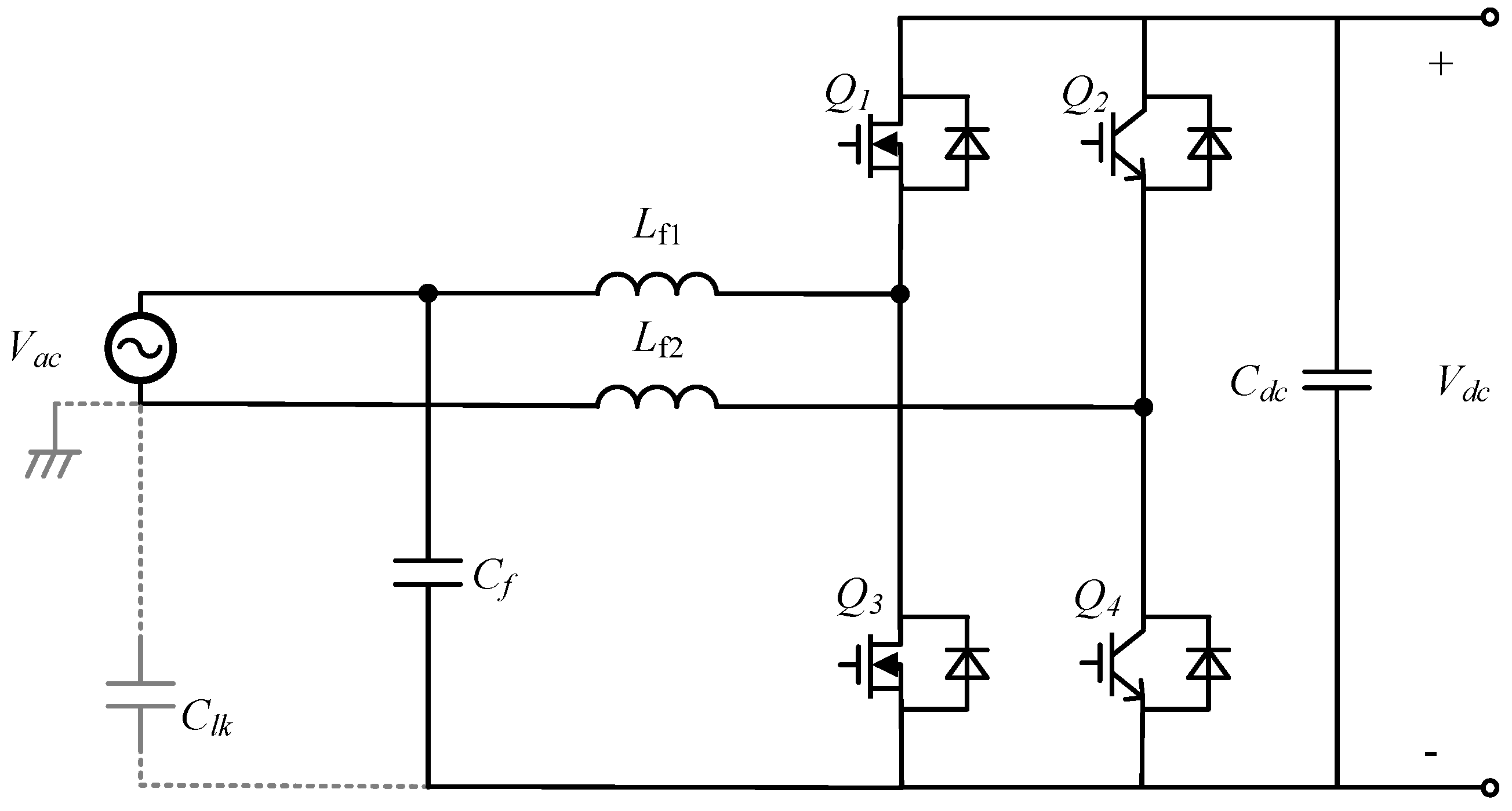
In this paper, a single-phase transformerless bidirectional PFC is studied, the configuration of which is shown in Figure 2. In Figure 2, it consists of a conventional full-bridge PFC and a capacitor Cf connecting the ac line terminal and a negative terminal of DC voltage, in which extra semiconductors are unnecessary. This PFC can mitigate the common-mode leakage current issue, since the inserted capacitor Cf provides a path to bypass the common-mode leakage current. In addition, the capacitor Cf combining the inductors in PFC converter can form LCL filter, which results a reduction in inductor current ripple. A hybrid modulation method is employed in this PFC. The unipolar switching scheme is applied to modulate the PFC converter; thus, two high-frequency switches and two low-frequency switches are required. Meanwhile, an additional modulation is inserted into the blank time of low-frequency switches when grid voltage is zero-crossing. This inserted modulation is to decrease the changing speed of the voltage on the capacitor Cf, which leads to a spike on the inductor current and leakage current. Therefore, this PFC can also achieve low cost and high efficiency.
The rest of this paper is structured as follows. Section 2 presents a detailed description of operating principle. The characteristics analysis results are presented in Section 3. System implementations are presented in Section 4. Experimental verification is presented in Section 5. Finally, Section 6 presents the main conclusions.

2. Analysis of Operating Principle

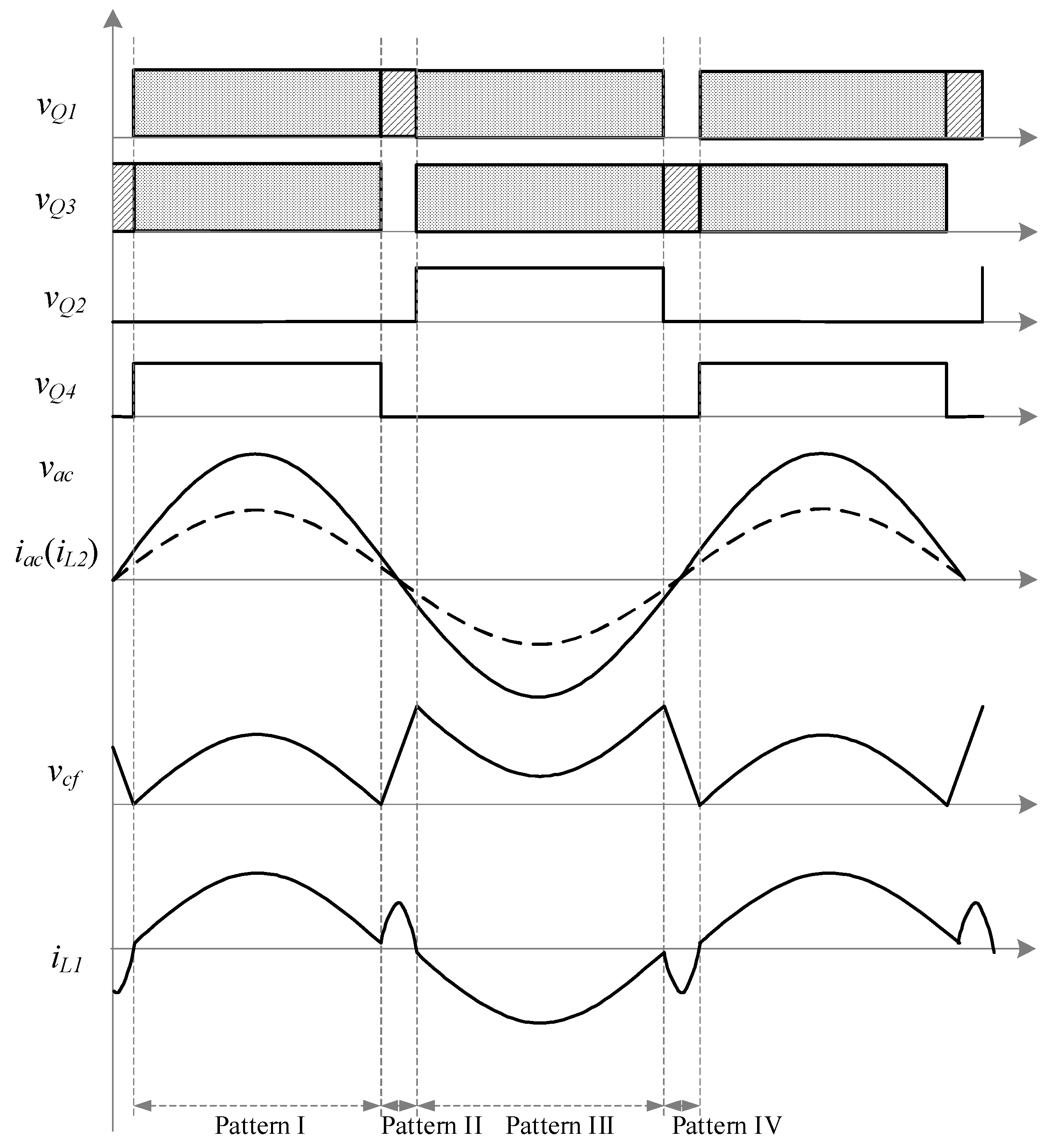
In Figure 2, Q1 and Q3 are required high-frequency switches, such as SiC MOSFETs, and Q2 and Q4 are required low-frequency switches, such as IGBTs. Switches Q1, Q2, Q3, and Q4 and inductors Lf1 and Lf2 form the conventional full-bridge PFC. Capacitor Clk represents the stray capacitor existing in the long cables which connect drive with motor. An additional capacitor Cf connects the ac line terminal and a negative terminal of DC voltage. Figure 3 shows the steady-state waveforms of the PFC, which exhibits Pattern I, Pattern II, Pattern III, and Pattern IV. The current conducting paths of every pattern are presented in Figure 4. For the convenience of the analysis, assumption that all switches, diodes, inductors, and capacitors are ideal.

2.1. Operation Pattern

(1)
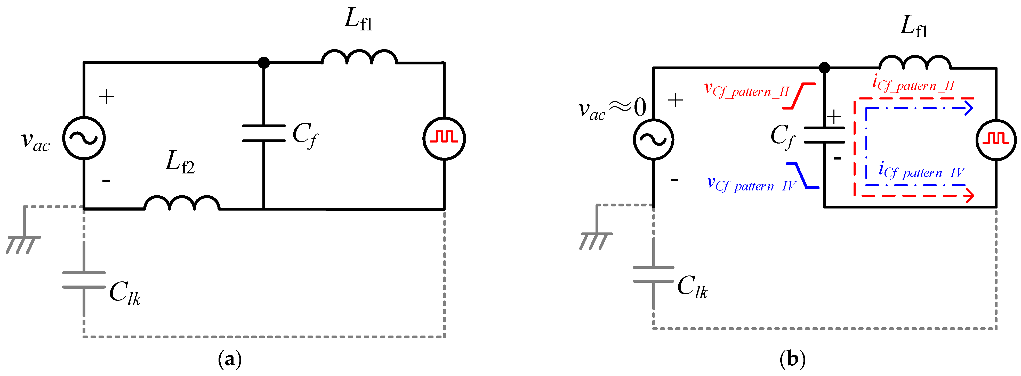
Pattern I: Switches Q1 and Q3 are switching complementarily with high frequency, and switch Q4 is constantly in the ON state when the grid voltage is in the positive half cycle. The switching state of Pattern I is shown in Figure 4a. It can be observed that the middle voltage of the high-frequency leg is high-frequency switching voltage with magnitude changing between Vdc and zero, which creates large high-frequency current ripple. Due to the capacitor Cf, connecting the ac line terminal and the negative terminal of the DC-side, the LCL filter is configured with the inductors Lf1 and Lf2, which act as the converter-side inductor and the grid-side inductor, respectively. The equivalent circuit of this pattern is shown in Figure 5a. As a result, a significant reduction in the inductor current ripple will be realized. In addition, it can be observed that the stray Clk is in parallel with the capacitor Cf when the grid is assumed to be short-circuit because it can be regarded as a constant voltage source in the high-frequency analysis. The impedance in the capacitor Cf path is lower. Capacitor Cf couples the voltage between the terminal of the grid-side and the negative terminal of the DC-side, which clamps the voltage difference, and the ripple voltage on the capacitor Cf is small. Therefore, the common-mode leakage current flow of the stray capacitor Clk is minimized.
(2)
Pattern II: Switches Q2 and Q4 are in the OFF state, switch Q1 switches ON or OFF with high frequency when the grid voltage zero-crossing point transitions from positive to negative. Switch Q3 acts as the synchronous switch of D3. The switching state of Pattern II is shown in Figure 4b. The reason for this pattern is that the middle voltage of the low-frequency leg changes rapidly from zero to Vdc if switches Q2 and Q4 switchover fast, while the voltages on capacitor Cf and stray capacitor Clk are approximately zero, the voltage difference on which will lead to a large spike on the inductor current and leakage current, which is unwanted. In this pattern, a similar buck converter is formed by DC voltage Vdc, switch Q1, diode D3 (synchronous switch Q3), inductor Lf1, capacitor Cf and stray capacitor Clk. The equivalent circuit of this pattern is shown in Figure 5b. The voltages on capacitor Cf and stray capacitor Clk will be charged up slowly to suppress the appearance of the current spike.
(3)
Pattern III: Switches Q1 and Q3 are switching complementarily with high frequency, and switch Q2 is constantly in the ON state when the grid voltage in the negative half cycle. The switching state of Pattern III is shown in Figure 4c. Although the inductor Lf2 is changed to connect the positive terminal of the DC-side, the LCL filter is formed by capacitor Cf, inductors Lf1 and Lf2, which achieves the low inductor current ripple. The equivalent circuit of this pattern is also shown in Figure 5a. Additionally, capacitor Cf and stray capacitor Clk are in parallel, which achieves low common-mode leakage current.
(4)
Pattern IV: Switches Q2 and Q4 are in the OFF state, switch Q3 switches ON or OFF with high frequency when the grid voltage zero-crossing point transitions from negative to positive. Switch Q1 acts the synchronous switch of D1. The switching state of Pattern IV is shown in Figure 4d. If switches Q2 and Q4 switchover fast, the middle voltage of the low-frequency leg changes rapidly from Vdc to zero, while the voltages on capacitor Cf and stray capacitor Clk are approximately Vdc, the voltage difference on which will also lead to a large spike on the inductor current and leakage current. In this pattern, a similar boost converter is formed by capacitor Cf and stray capacitor Clk, inductor Lf1, switch Q3, diode D1 (synchronous switch Q1), and DC voltage Vdc. The equivalent circuit of this pattern is shown in Figure 5b. The voltages on capacitor Cf and stray capacitor Clk will be discharged slowly to suppress the appearance of the current spike.

2.2. Control Scheme

Figure 6 presents the control block diagram of the PFC. The pattern selection is based on the polar and the trend of the grid voltage.
For Pattern I and Pattern III, a basic double-loop control methodology is applied. DC voltage Vdc is regulated by a proportional integral (PI) controller in the outer loop. The output of outer loop is the grid current reference iac_ref of the inner loop, which realizes to track the grid current iac in sinusoidal by PI controller. The output of inner loop is used to generate the PWM signals of switches Q1 and Q3 for Pattern I and Pattern III. The signals of switches Q2 and Q4 are controlled by the polar of grid voltage Vac. Switch Q4 remains in the ON state at the positive half grid cycle for Pattern I, and switch Q2 remains in the ON state at the negative half grid cycle for Pattern III.
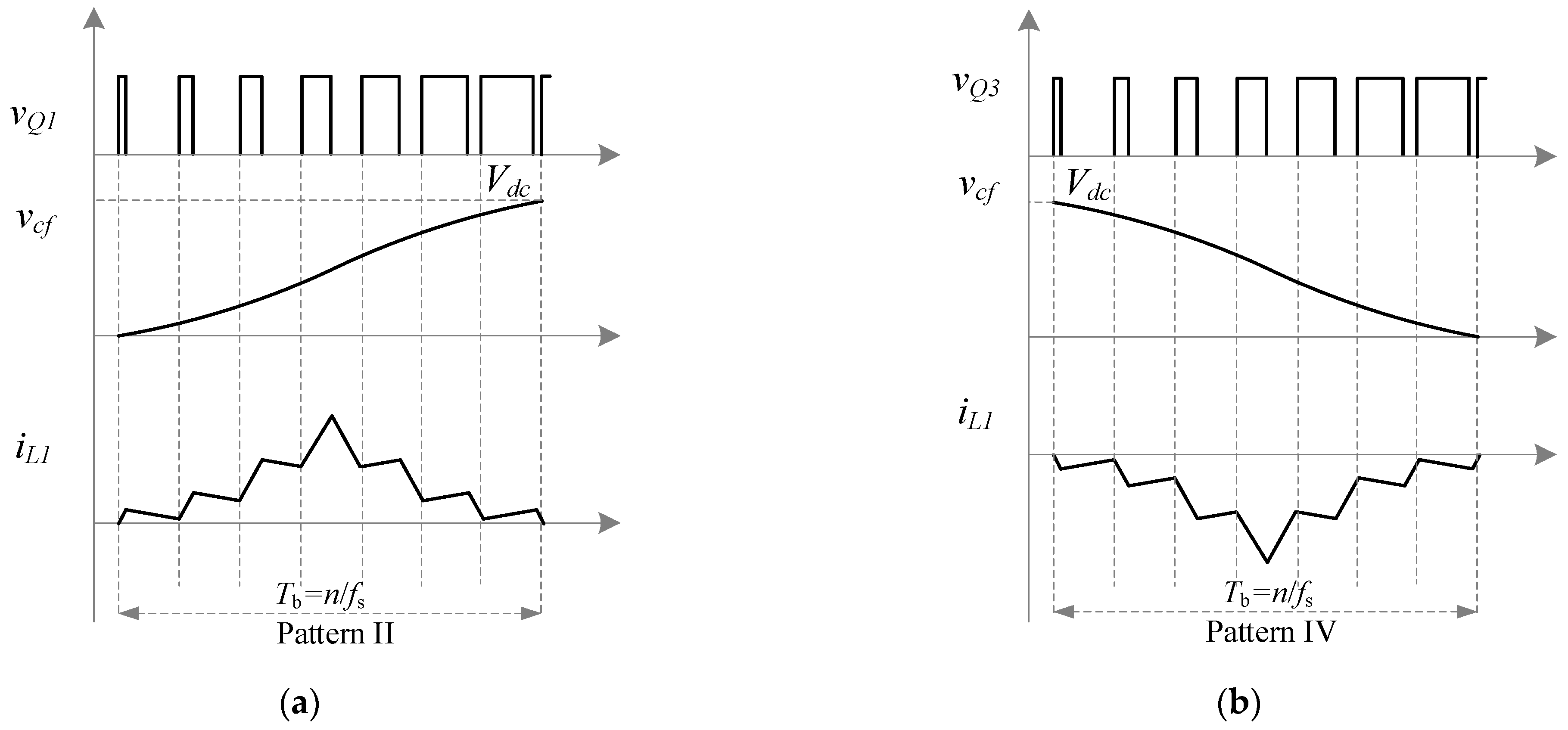
For Pattern II or Pattern IV, switches Q1 or Q3 operate at high-frequency ON or OFF, and are controlled by the open-loop control. The frequency Q1 and Q3 are same with Pattern I and Pattern III, and the duty ratio expands gradually to decrease the changing speed of voltage on the capacitor Cf and stray capacitor Clk, which will lead to a spike on the inductor current and leakage current. The zoomed-in waveforms in Pattern II or Pattern IV are shown in Figure 7. Note that switches Q1 and Q3 switch complementarily in Pattern II or Pattern IV to decrease the losses of diodes D1 and D3.

3. Characteristics Analysis

The characteristics of this single-phase bidirectional transformerless PFC are analyzed based on Figure 5. The inductors Lf1 and Lf2 are identical and have the same values. The positive half grid cycle is used for the following analysis; the negative half grid cycle has the same characteristics, which are not present in this paper.

3.1. Duty Cycle

In Pattern I and Pattern III, the PFC works as a simple boost converter when neglecting the small voltage drop on the grid-side inductor Lf2. Thus, the duty ratio can be expressed by
D I ,   III = 1 v ac ( t ) V dc
where vac is the instantaneous grid voltage, vac = Vacsin(ωt), Vac is the peak amplitude of grid voltage, and ω is the angular grid frequency. The duty ratio can be obtained as
D I ,   III = 1 V ac V dc sin ω t
At all times, the duty cycle is time varying and follows the change of grid voltage.
In Pattern II or Pattern IV, a similar buck or boost converter is formed to charge or discharge slowly the capacitor Cf and stray capacitor Clk. The duty ratio of the switches Q1 or Q3 can be expressed as
D II ,   IV = ( n 1 ) Δ D
where ∆D is the incremental step of the duty ratio, and n is the number of switching periods in Pattern II or Pattern IV, n = 1,2,3…, which are always set in the digital controller. When the duty ratio of the switches Q1 or Q3 expands gradually to 1, the Pattern II or Pattern IV finish the modulation.

3.2. Current Ripple and Voltage Ripple of LCL Filter in Pattern I and Pattern III

Under fixed switching frequency and continuous conduction mode operation, the converter-side inductor current ripple is developed from the ON-state characteristic as
Δ i L 1 _ I ,   III = ( V dc V ac sin ω t ) V ac sin ω t V dc L 1 f s
where fs is the switching frequency of switches Q1 and Q3.
The voltage ripple of the capacitor Cf is mainly contributed by the current ripple of the converter-side inductor, which is calculated as
Δ v cf _ I ,   III = ( V dc V ac sin ω t ) V ac sin ω t 8 V dc L 1 ( C lk + C f ) f s 2
The grid current ripple is basically contributed by the capacitor Cf and stray capacitor Clk, thus, the grid current ripple is formed as
Δ i L 2 _ I ,   III = ( V dc V ac sin ω t ) V ac sin ω t 16 π V dc ( C lk + C f ) L 1 2 f s 3

3.3. Duty Cycle Fundamental Current of Inductor L1 in Pattern II and Pattern IV

The current spike caused by charging or discharging the capacitor Cf and stray capacitor Clk is suppressed by inserting a modulation of switches Q1 or Q3 at the blank time between Q2 and Q4. The transition of the voltage on capacitor Cf and stray capacitor Clk in Pattern II and Pattern IV can be approximately treated, as shown in the following formulas,
v cf _ II = 1 2 V dc ( 1 cos ω b t )
v cf _ IV = 1 2 V dc ( 1 + cos ω b t )  
where ωb is the equivalent angular frequency of the blank time, ωb = πfs/n. In Pattern II or Pattern IV, the current of inductor L1 is the charging or discharging current for capacitor Cf and stray capacitor Clk. The fundamental current of inductor L1 can be approximately calculated as a derivation of vcf, which are
i L 1 _ II = ω b ( C lk + C f ) V dc 2 sin ω b t
i L 1 _ IV = ω b ( C lk + C f ) V dc 2 sin ω b t  

3.4. Current Ripple and Voltage Ripple of LCL Filter in Pattern I and Pattern III

The common-mode leakage current is defined as the current passing through the stray capacitor on the cable and the ground. As shown in Figure 2, the stray capacitor Clk is virtually parallel with the capacitor Cf. In Pattern I and Pattern III, the high-frequency part of iL1 passes through the capacitor Cf and the stray capacitor Clk. In Pattern II and Pattern IV, current iL1 charges or discharges the capacitor Cf and the stray capacitor Clk together; thus, the common-mode leakage current can be expressed as
Δ i C lk = C lk C f + C lk Δ i L 1
Based on (11), the common-mode leakage current is directly proportional to the capacitance ratio between capacitor Cf and stray capacitor Clk, and the converter-side inductor current ripple ∆iL1. In Pattern I and Pattern III, the common-mode leakage current can be adjusted by the value of capacitor Cf. However, in Pattern II and Pattern IV, capacitor Cf and blank time between Q2 and Q4 need to be traded off to suppress the spike on inductor current iL1 and THDi of the PFC.

4. System Implementation

4.1. Topology Variants

Figure 2 shows one of the possible single-phase bidirectional transformerless PFCs; the alternative configurations are shown in Figure 8, which have same electrical characteristics, except the DC voltage offset across capacitor Cf, because three variants connect the capacitor Cf to Vdc minus, half Vdc, or Vdc plus, respectively.

4.2. System Implementation

A hardware setup to evaluate the PFC in the laboratory. Table 1 shows the key parameters of hardware setup. A 47nF capacitor is used to simulate the stray capacitor Clk. This prototype is used to verify the performances of the PFC.

4.3. Selection of Filter Components

In the design, the inductor current ripple is set to 20% of peak current at full power. Based on (4), the minimum value of the required inductance is calculated as 0.12 mH. Considering both the inductance drop due to nanocrystalline material and experimental performance, inductor Lf1 and Lf2 are designed as 0.17 mH. The selection of Cf is based on the following two criteria: one is the LCL filter resonance frequency, which should be a large ratio difference from the switching frequency, such as a tenfold difference; the other is the common-mode leakage current, which should meet some standards to limit the leakage current to a certain level. To fulfill both criteria, the value of capacitor Cf is selected as 6.8 μF based on the parameters in Table 1.

4.4. Simulation Verification

To verify the operating principle of the PFC, the simulation model is generated in PLECS. In addition, the comparisons between the prior PFCs in [18,26] and the PFC in this paper are presented in this section.
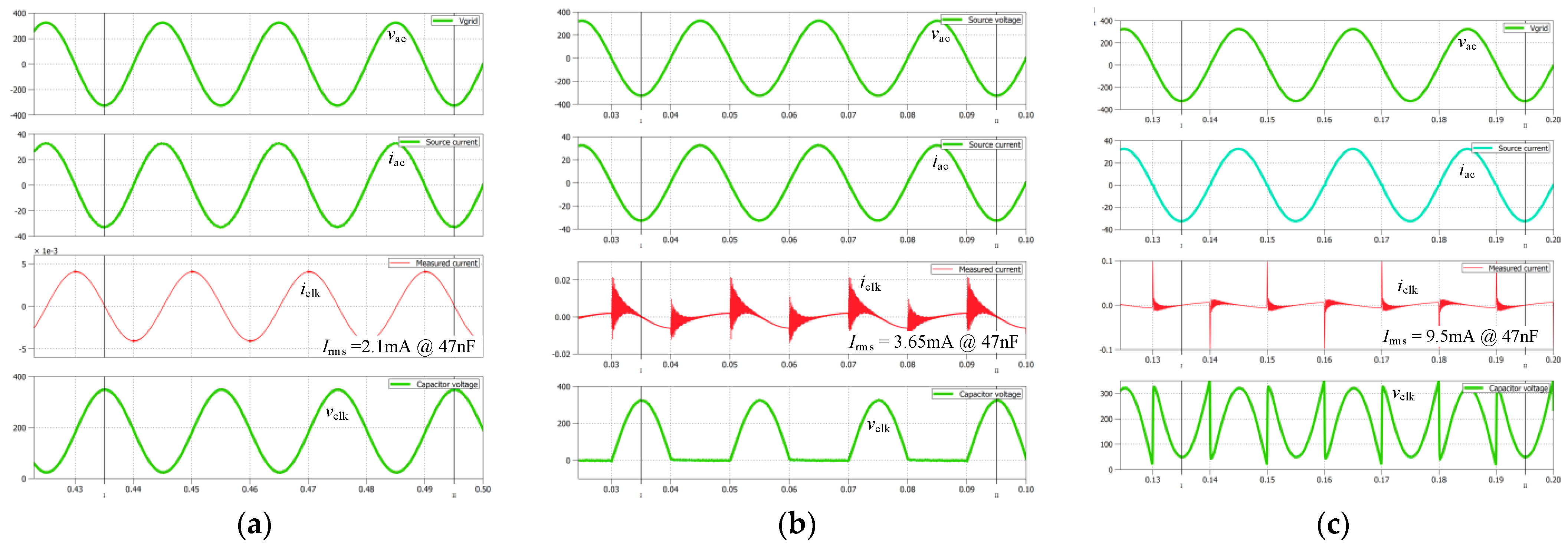
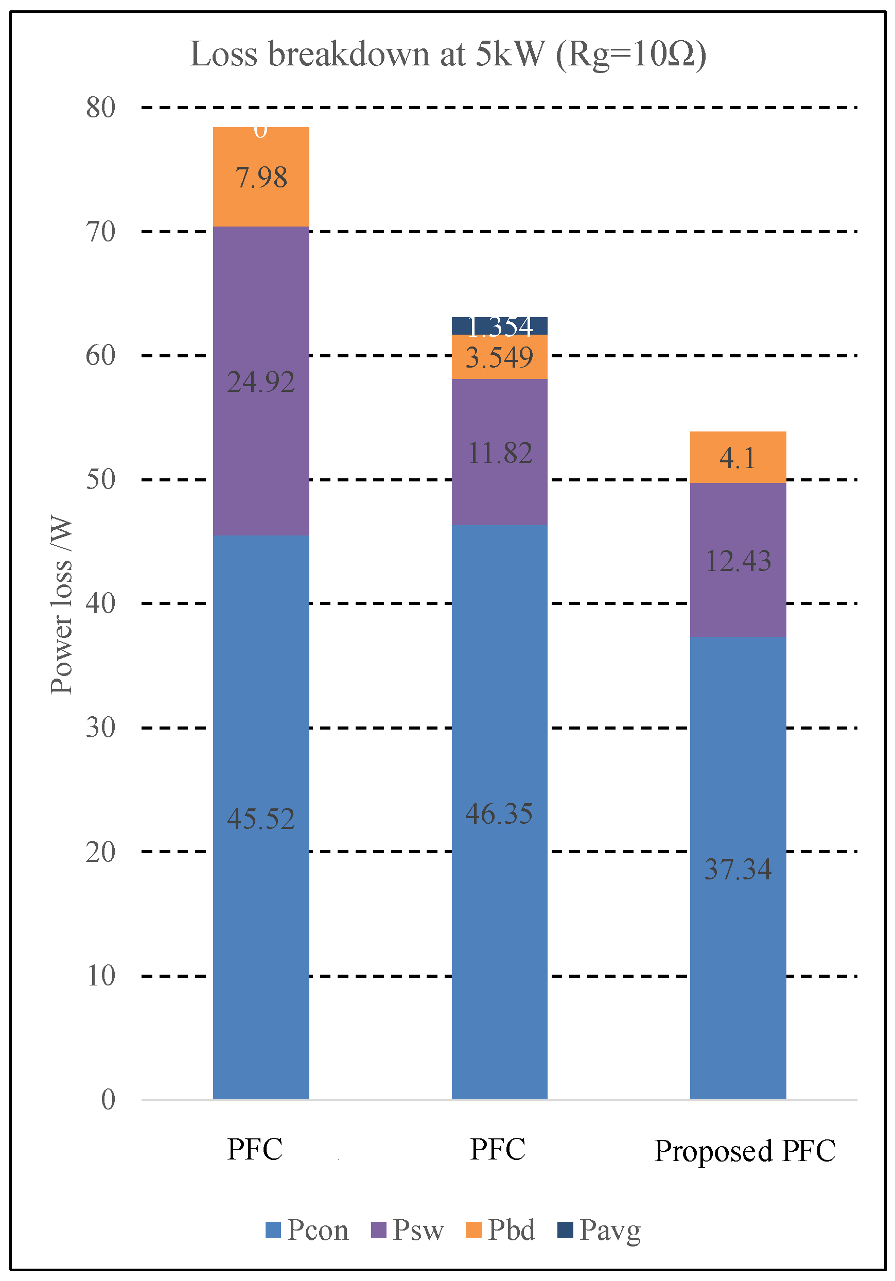
The PFC in [18] is the conventional full-bridge PFC with the bipolar switching scheme. The PFC with AVG in [26] is the conventional full-bridge PFC with one added capacitor and two bidirectional semiconductors, which uses the unipolar switching scheme. The compared simulation results are shown in Figure 9, in which the grid voltage vac, the grid current iac (iL2), the common-mode leakage current iClk, and the capacitor voltage vClk are presented. The capacitor current iClk is used to represent the common-mode leakage current. The parameters of the PFCs in simulation models are same with Table 1. Based on the simulation results in Figure 9, the common-mode leakage current of the PFC in this paper is higher than others, but it meets the requirement of 300 mA [10,11,12]. Figure 10 presents the simulation semiconductor losses of the prior PFCs in [18,26] and the PFC in this paper. The high-frequency switches use C3M0065100K from Cree Inc., Durham, NC, USA, and the low-frequency switches use IKW75N65EL5 from Infineon Inc., Ilmenau, Germany. The simulation semiconductor losses include the conduction losses and the switching losses of switches of the full-bridge PFC, the losses of body diodes, and the losses of switches on AVG. From Figure 10, the simulation semiconductor losses of the PFC in this paper are much lower than those of the prior PFCs. What is more, the PFC in this paper has no additional semiconductors and only two high-frequency switches, which can be acquired at low cost.

5. Experimental Verification

Experiments of the PFC are implemented on a 5 kW prototype to demonstrate the performance; the design guidelines are provided in Section 4.
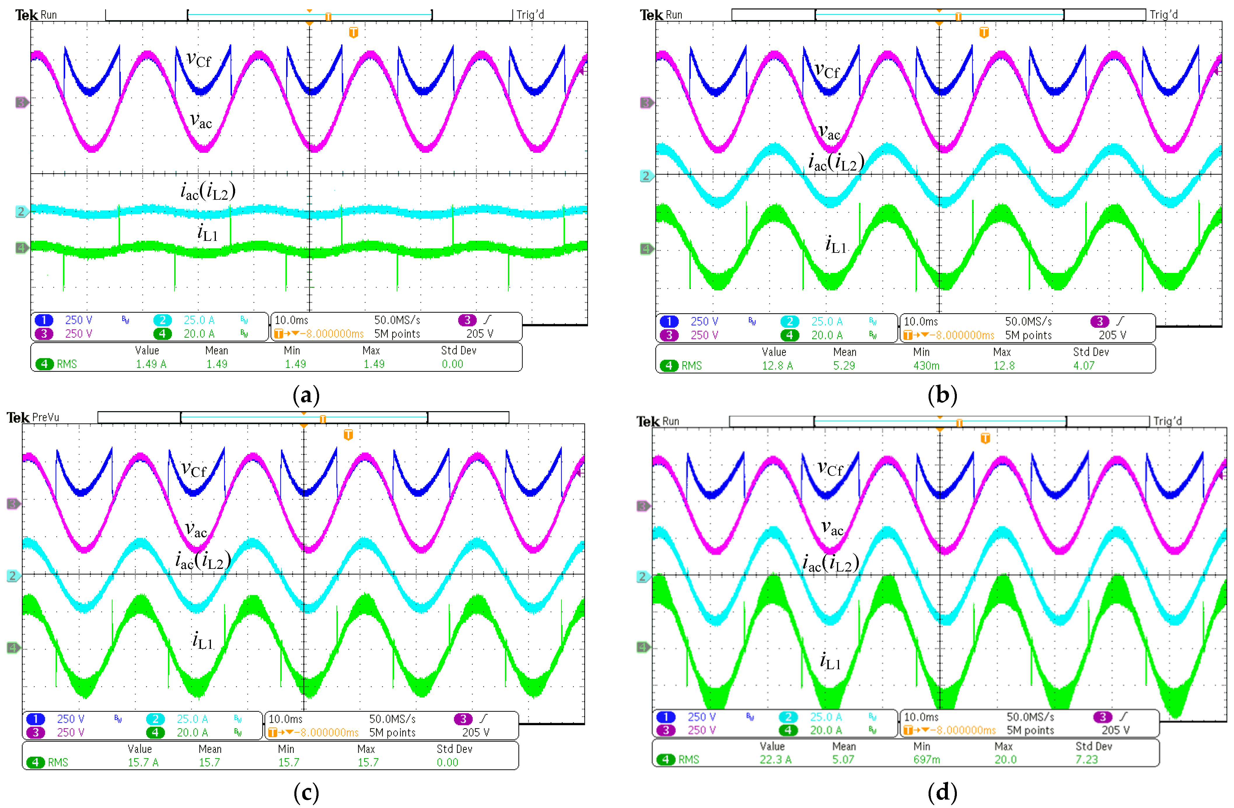
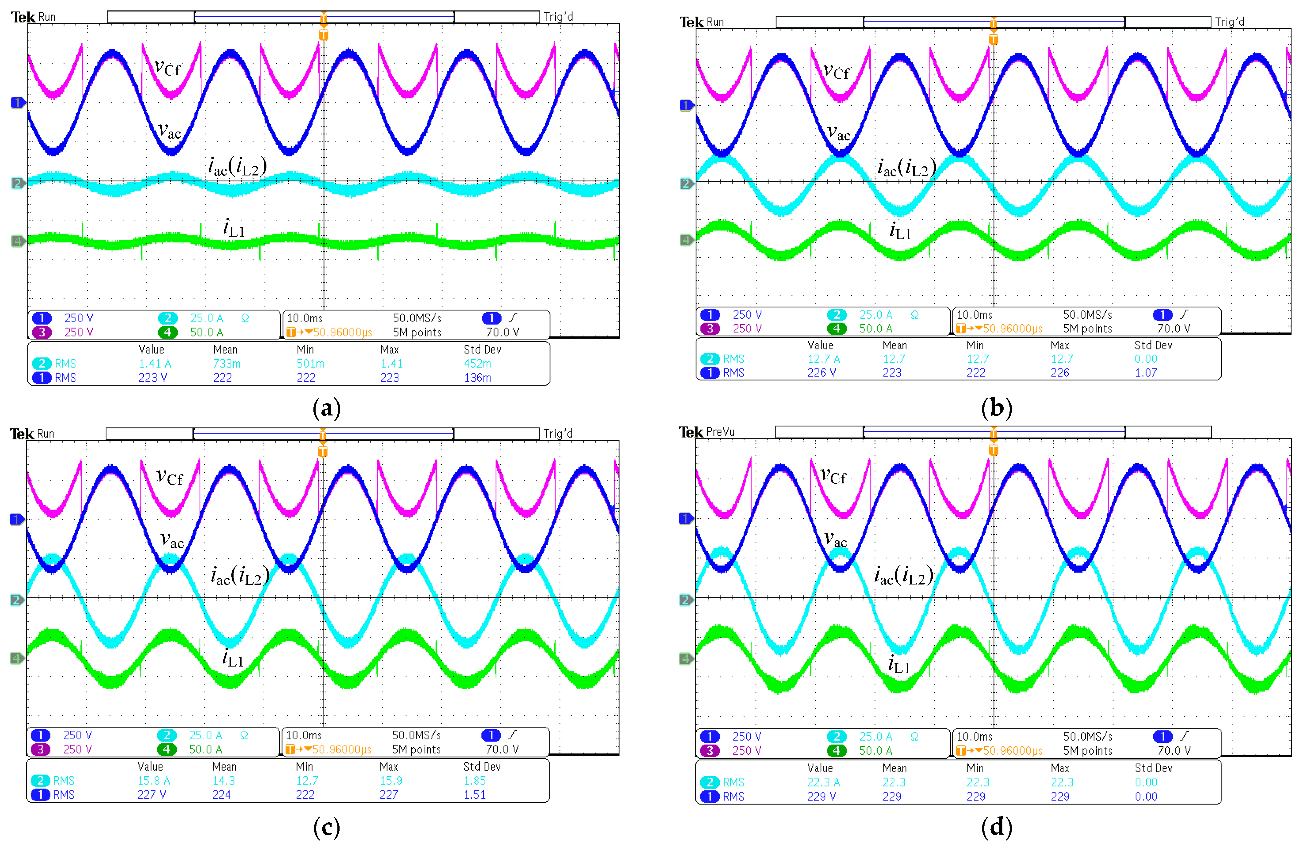
Figure 11 and Figure 12 presents the steady-state performances of the PFC under different conditions. Figure 11 presents the experimental results at PFC mode. Figure 12 presents the experimental results at inverter mode. The prototype is tested under grid voltage 230 V and DC voltage 370 V, with power levels of 0.5 kW, 1 kW, 2.5 kW, and 5 kW. In Figure 11 and Figure 12, the grid voltage vac, the grid current iac (iL2), the capacitor voltage vCf, and the inductor current iL1 are presented. As seen in Figure 11 and Figure 12, the converter-side inductor current iL1 and the grid-side current iac (iL2) varied under different power level conditions. The voltage on the capacitor Cf changed by Vdc when Q2 and Q4 switched complementarily according to the polarity of grid voltage. Due to the inserted modulation into the blank time of switches Q2 and Q4, the changing speed of voltage on the capacitor Cf was low, and the spike on the current of inductor Lf1 was also low. Because the LCL filter was configured at the grid-side, no spike is present on the grid-side current iac (iL2).
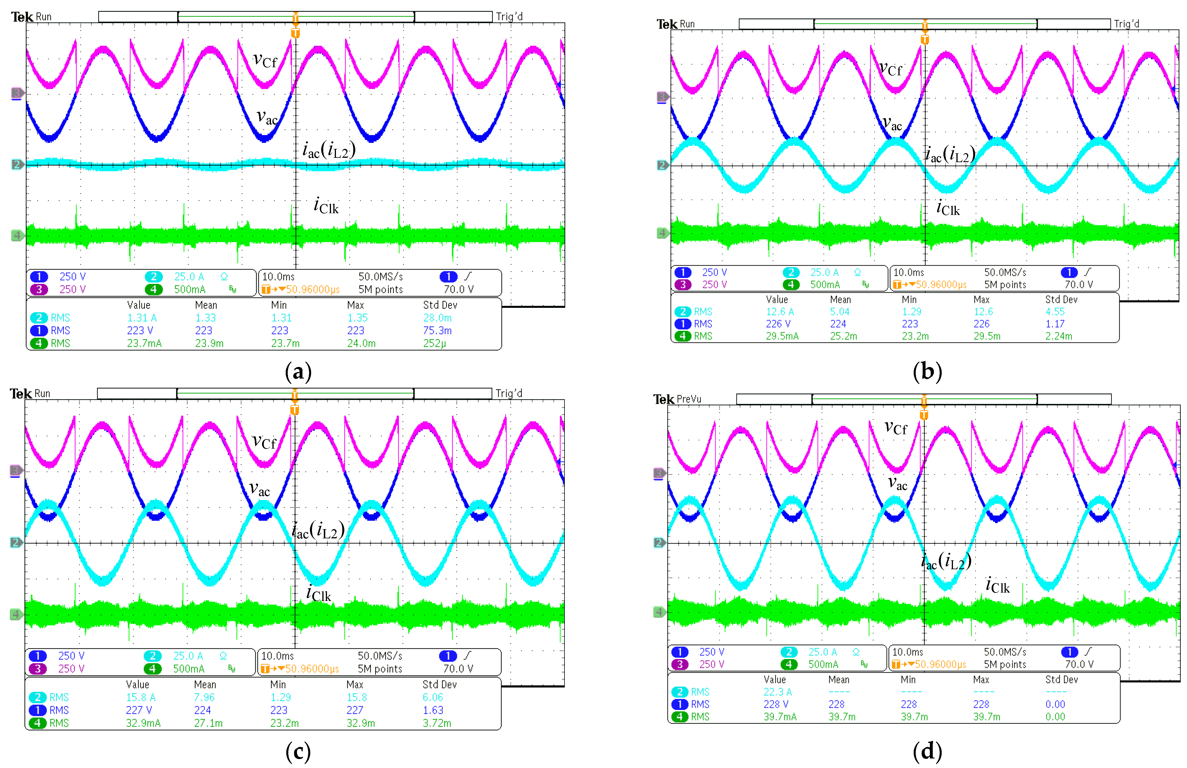
Figure 13 presents the common-mode leakage current performance of the PFC. The prototype is tested under grid voltage 230 V and DC voltage 370 V, with power levels of 0.5 kW, 1 kW, 2.5 kW and 5 kW. In Figure 13, the grid voltage vac, the grid current iac (iL2), the capacitor voltage vClk, and the common-mode leakage current iClk are presented. A 47nF capacitor was used to simulate the stray capacitor [27,28,29]. The capacitor current iClk was used to represent the common-mode leakage current. During each half grid cycle, small spikes on the common-mode leakage current appeared during the blank time of low-frequency switches Q2 and Q4. These results prove that the common-mode leakage current was able to be controlled into the mA range, which was accepted by standards.
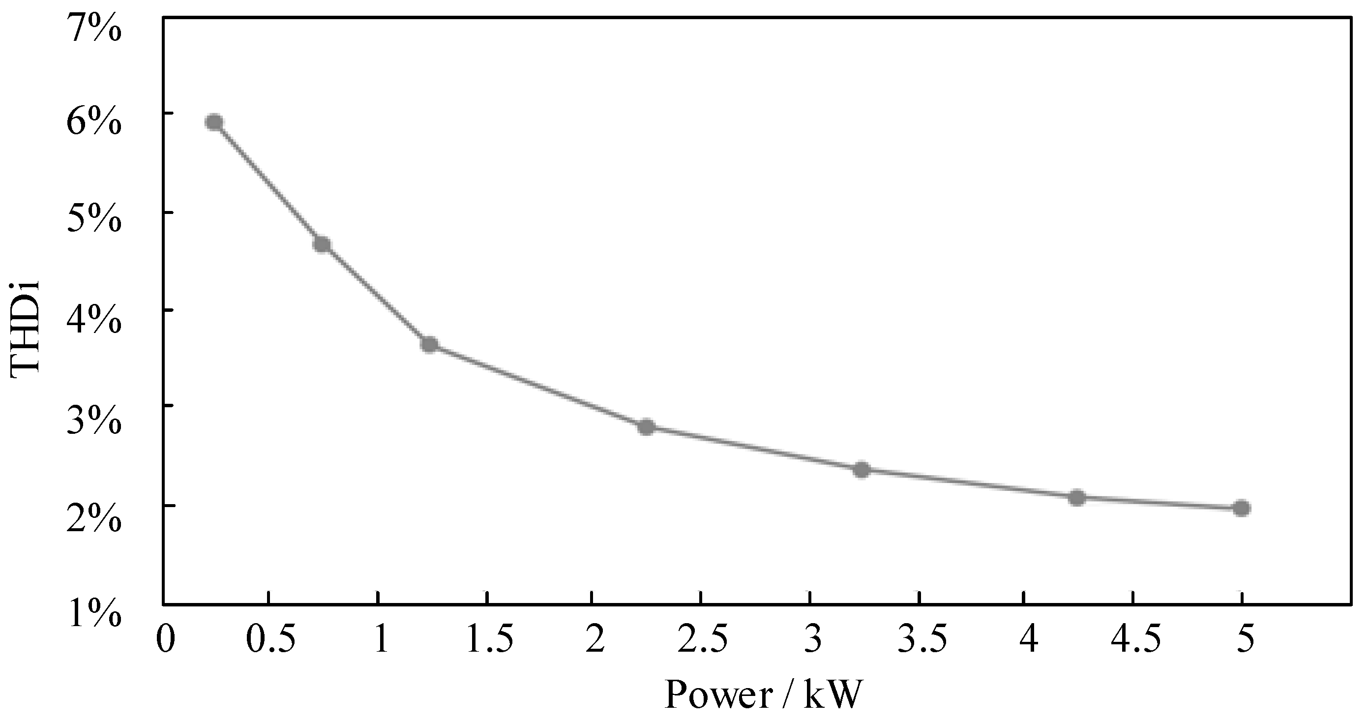
Figure 14 presents the experimental efficiency of the PFC. In Figure 14, the power is from 0.2 kW to 5 kW. The lowest efficiency is 94.12% when the power is 0.2 kW. The highest efficiency is 98% when the power is 2 kW. The efficiency of the full power is 97.22%. Additionally, the total harmonics distortion (THD) at different power levels are also attained, as shown in Figure 15, which demonstrates that the THD at 5 kW is less than 2%.

6. Conclusions

This paper evaluates a single-phase bidirectional and transformerless PFC associated with hybrid modulation method. This PFC not only mitigates the common-mode leakage current issue, but also builds an LCL filter to reduce the inductor current ripple. A hybrid modulation method is employed in this PFC. The unipolar switching scheme and the addition of another modulation inserted into the blank time of low-frequency switches are combined. This hybrid modulation method guarantees the high efficiency and the suppression effectiveness on the common-mode leakage current. The operating principles of the PFC are analyzed in detail. The performances of the PFC are verified by experiments.

Author Contributions

Conceptualization, M.L.; methodology, M.L.; validation, M.L.; writing, M.L.; writing—review and editing, P.J. and T.G.; funding acquisition, P.J. All authors have read and agreed to the published version of the manuscript.

Funding

This research was funded by National Natural Science Foundation of China, grant number 51907002.

Data Availability Statement

Not applicable.

Conflicts of Interest

The authors declare no conflict of interest. The funders had no role in the design of the study; in the collection, analyses, or interpretation of data; in the writing of the manuscript; or in the decision to publish the results.

References

  1. Chen, F.; Burgos, R.; Boroyevich, D. A Bidirectional High-Efficiency Transformerless Converter with Common-Mode Decoupling for the Interconnection of AC and DC Grids. IEEE Trans. Power Electron. 2019, 34, 1317–1333. [Google Scholar] [CrossRef]
  2. Singh, S.M.; Gaurav, T.; Singh, H. PFC Cuk Converter Fed PMBLDC Motor for Ceiling Fan. In Proceedings of the 2021 International Conference on Communication, Control and Information Sciences (ICCISc), Idukki, India, 16–18 June 2021; pp. 1–5. [Google Scholar]
  3. Liu, J.; Tian, H.; Liang, G.; Zeng, J. A bridgeless electrolytic capacitor-free LED driver based on series-resonant converter with constant frequency control. IEEE Trans. Power Electron. 2019, 34, 2712–2725. [Google Scholar] [CrossRef]
  4. Strothmann, B.; Schafmeister, F.; Bocker, J. Common-Mode-Free Bidirectional Three-Phase PFC-Rectifier for Non-Isolated EV Charger. In Proceedings of the 2021 IEEE Applied Power Electronics Conference and Exposition (APEC), Phoenix, AZ, USA, 14–17 June 2021; pp. 2783–2790. [Google Scholar]
  5. Fernandes, L.G.; Badin, A.A.; Cortez, D.F.; Gules, R.; Romaneli, E.F.R.; Assef, A. Transformerless UPS System Based on the Half-Bridge Hybrid Switched-Capacitor Operating as AC–DC and DC–DC Converter. IEEE Trans. Ind. Electron. 2021, 68, 2173–2183. [Google Scholar] [CrossRef]
  6. Siu, K.K.M.; Ho, C.N.M. A critical review of Bridgeless PFC boost rectifiers with common-mode voltage mitigation. In Proceedings of the IECON 2016—42nd Annual Conference of the IEEE Industrial Electronics Society, Florence, Italy, 23–26 October 2016; pp. 3654–3659. [Google Scholar]
  7. Sun, Y.; Liu, Y.; Su, M.; Xiong, W.; Yang, J. Review of active power decoupling topologies in single-phase systems. IEEE Trans. Power Electron. 2016, 31, 4778–4794. [Google Scholar] [CrossRef]
  8. Tian, H.; Chen, M.; Liang, G.; Xiao, X. Single-Phase Rectifier with Reduced Common-Mode Current, Auto-PFC, and Power Decoupling Ability. IEEE Trans. Power Electron. 2022, 37, 6873–6882. [Google Scholar] [CrossRef]
  9. Siu, K.K.M.; Ho, C.N.M.; Li, R.T.H. A Four-Quadrant Single-Phase Grid-Connected Converter with Only Two High-Frequency Switches. IEEE Trans. Ind. Electron. 2020, 67, 1899–1909. [Google Scholar] [CrossRef]
  10. DIN VDE V 0126-1-1; Automatic Disconnection Device between a Generator and the Public Low Voltage Grid. VDE: Berlin, Germany, 2006.
  11. IEC Standard 61008-1-2010; Residual Current Operated Circuit-Breakers without Integral Overcurrent Protection for Household and Similar Uses (RCCBs)—Part 1: General Rules. IEC: Geneva, Switzerland, 2010.
  12. IEC Standard 62109-1-2007; Safety of Power Converters for Use in Photovoltaic Power Systems—Part 1: General Requirement. IEC: Geneva, Switzerland, 2007.
  13. Vosoughi, N.; Hosseini, S.H.; Sabahi, M. A New Single-Phase Transformerless Grid-Connected Inverter with Boosting Ability and Common Ground Feature. IEEE Trans. Ind. Electron. 2020, 67, 9313–9325. [Google Scholar] [CrossRef]
  14. Peng, F.; Zhou, G.; Xu, N.; Gao, S. Zero Leakage Current Single-Phase Quasi-Single-Stage Transformerless PV Inverter with Unipolar SPWM. IEEE Trans. Power Electron. 2022, 37, 13755–13766. [Google Scholar] [CrossRef]
  15. Xiao, H.F.; Lan, K.; Zhang, L. A quasi-unipolar SPWM full-bridge transformerless PV grid-connected inverter with constant common-mode voltage. IEEE Trans. Power Electron. 2015, 30, 3122–3132. [Google Scholar] [CrossRef]
  16. Do, N.; Huang, B.; Nguyen, T.; Wu, J.; Liu, Y.; Chiu, H. An Efficiency-Optimized Totem-pole Bridgeless Power Factor Correction Regulator using GaN HEMTs. In Proceedings of the 2020 International Symposium on Computer, Consumer and Control (IS3C), Taichung City, Taiwan, 13–16 November 2020; pp. 351–355. [Google Scholar]
  17. Yang, B.; Li, W.; Gu, Y.; Cui, W.; He, X. Improved transformerless inverter with common-mode leakage current elimination for a photovoltaic grid-connected power system. IEEE Trans. Power Electron. 2012, 27, 752–762. [Google Scholar] [CrossRef]
  18. Fan, J.; Yeung, R.; Chung, H. Optimized hybrid PWM scheme for mitigating zero-crossing distortion in totem-pole bridgeless PFC. IEEE Trans. Power Electron. 2019, 34, 928–942. [Google Scholar] [CrossRef]
  19. Victor, M.; Greizer, F.; Bremicker, S.; Hubler, U. Method of Converting a Direct Current Voltage from a Source of Direct Current Voltage, more Specifically from a Photovoltaic Source of Direct Current Voltage, into a Alternating Current Voltage. U.S. Patent US7411802 B2, 12 August 2008. [Google Scholar]
  20. Freddy, T.K.S.; Lee, J.; Moon, H.-C.; Lee, K.-B.; Rahim, N.A. Modulation technique for single-phase transformerless photovoltaic inverters with reactive power capability. IEEE Trans. Ind. Electron. 2017, 64, 6989–6999. [Google Scholar] [CrossRef]
  21. Liu, B.; Su, M.; Yang, J.; Song, D.; He, D.; Song, S. Combined Reactive Power Injection Modulation and Grid Current Distortion Improvement Approach for H6 Transformer-Less Photovoltaic Inverter. IEEE Trans. Energy Convers. 2017, 32, 1456–1467. [Google Scholar] [CrossRef]
  22. Rahman, M.M.; Hossain, M.S.; Talukder, M.S.I.; Uddin, M.N. Transformerless Six-Switch (H6)-Based Single-Phase Inverter for Grid-Connected Photovoltaic System with Reduced Leakage Current. IEEE Trans. Ind. Appl. 2021, 58, 974–985. [Google Scholar] [CrossRef]
  23. Tang, Z.; Su, M.; Sun, Y.; Cheng, B.; Yang, Y.; Blaabjerg, F.; Wang, L. Hybrid UP-PWM Scheme for HERIC Inverter to Improve Power Quality and Efficiency. IEEE Trans. Power Electron. 2019, 34, 4292–4303. [Google Scholar] [CrossRef] [Green Version]
  24. Schmidt, H.; Siedle, C.; Ketterer, J. DC/AC Converter to Convert Direct Electric Voltage into Alternating Voltage or into Alternating Current. U.S. Patent US7046534 B2, 16 May 2006. [Google Scholar]
  25. Ho, C.N.M.; Li, R.T.-H.; Siu, K.K.-M. Active Virtual Ground—Bridgeless PFC Topology. IEEE Trans. Power Electron. 2017, 32, 6206–6218. [Google Scholar] [CrossRef]
  26. Ho, R.; Li, C.; Chen, E. Active virtual ground—Single-phase transformerless grid-connected voltage source inverter topology. IEEE Trans. Power Electron. 2018, 33, 1335–1346. [Google Scholar]
  27. Wang, S.; Kong, P.; Lee, F.C. Common mode noise reduction for boost converters using general balance technique. IEEE Trans. Power Electron. 2007, 22, 1410–1416. [Google Scholar] [CrossRef]
  28. Zhu, X.; Wang, H.; Zhang, W.; Wang, H.; Deng, X.; Yue, X. A Single-Phase Five-Level Transformer-Less PV Inverter for Leakage Current Reduction. IEEE Trans. Ind. Electron. 2022, 69, 3546–3555. [Google Scholar] [CrossRef]
  29. Xie, L.; Yuan, X. Common-Mode Current Reduction at DC and AC Sides in Inverter Systems by Passive Cancellation. IEEE Trans. Power Electron. 2021, 36, 9069–9079. [Google Scholar] [CrossRef]
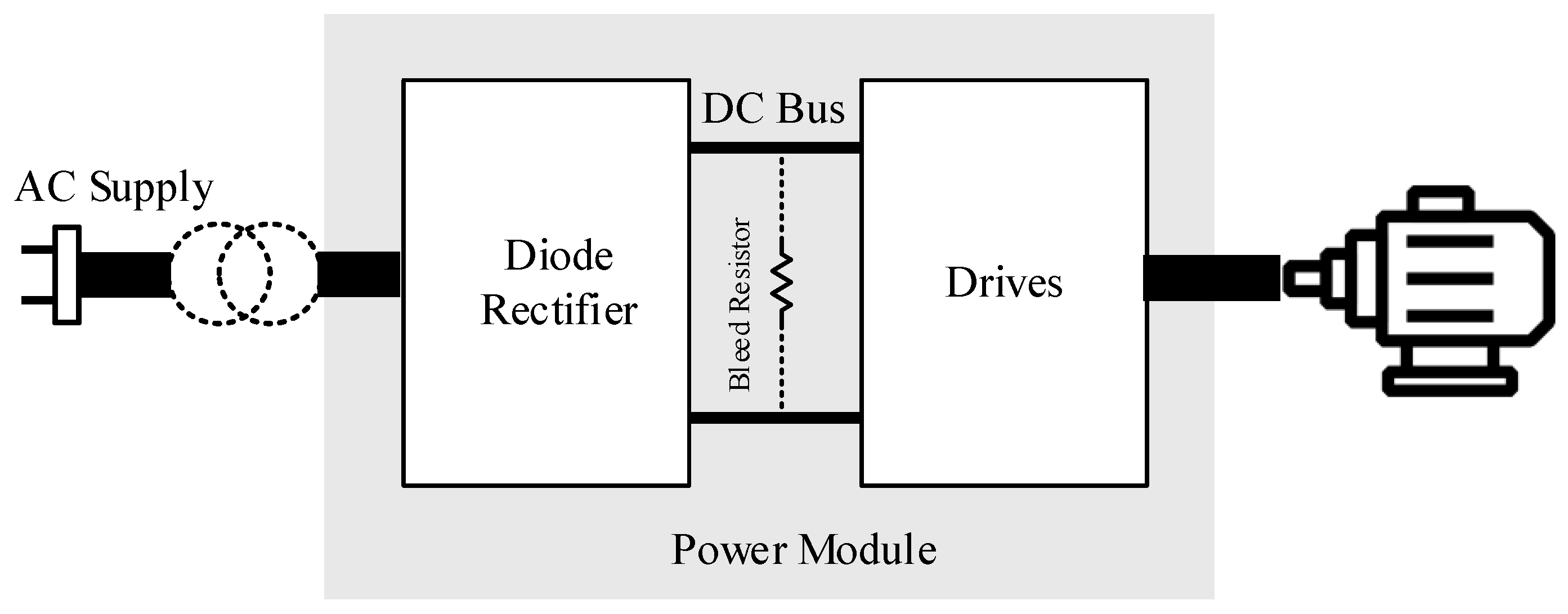
Figure 1. Traditional configuration for low-power servo motor drive application.
Energies 15 08329 g001
Figure 2. Configuration of PFC topology.
Energies 15 08329 g002
Figure 3. Steady-state waveforms of the PFC.
Energies 15 08329 g003
Figure 4. The current conducting path of every pattern. (a) Pattern I, (b) Pattern II, (c) Pattern III, and (d) Pattern IV.
Energies 15 08329 g004
Figure 5. Equivalent circuit of every pattern. (a) Pattern I and Pattern III, (b) Pattern II and Pattern IV.
Energies 15 08329 g005
Figure 6. Control diagram of the single-phase bidirectional transformerless PFC.
Energies 15 08329 g006
Figure 7. The zoomed-in waveform during the grid voltage zero-crossing. (a) Pattern II and (b) Pattern IV.
Energies 15 08329 g007
Figure 8. Possible configurations of the single-phase bidirectional transformerless PFC. (a) Cf connecting to Vdc plus and (b) Cf half Vdc minus.
Energies 15 08329 g008
Figure 9. Simulation results of the prior PFCs in [18,26] and the PFC in this paper. (a) Conventional full-bridge PFC with bipolar switching scheme in [18], (b) conventional full-bridge PFC with AVG in [26], and (c) PFC in this paper.
Energies 15 08329 g009
Figure 10. Simulation semiconductor losses of the prior PFCs in [18,26] and the PFC in this paper.
Energies 15 08329 g010
Figure 11. Steady-state waveforms of the PFC at PFC mode. (a) 0.5 kW, (b) 1 kW, (c) 2.5 kW, and (d) 5 kW.
Energies 15 08329 g011
Figure 12. Steady-state waveforms of PFC at Inverter mode. (a) 0.5 kW, (b) 1 kW, (c) 2.5 kW, and (d) 5 kW.
Energies 15 08329 g012
Figure 13. Common leakage current performance of the PFC. (a) 0.5 kW, (b) 1 kW, (c) 2.5 kW, and (d) 5 kW.
Energies 15 08329 g013
Figure 14. Efficiency of the PFC at different power levels.
Energies 15 08329 g014
Figure 15. Total harmonics distortion (THD) at different power levels.
Energies 15 08329 g015
Table 1. Key parameters of hardware setup.
ParametersValues
DC voltage370 V
Grid voltage230 V
Grid frequency50 Hz
Power5 kW
Switching frequency60 kHz
Blank Time of Pattern II or IV120 μs
Stray Capacitor47 nF
Publisher’s Note: MDPI stays neutral with regard to jurisdictional claims in published maps and institutional affiliations.