Article

Design and Control of a Quasi-Z Source Multilevel Inverter Using a New Reaching Law-Based Sliding Mode Control

1
Department of Electrical Power Engineering, USPCAS-E, National University of Sciences and Technology (NUST), Islamabad 44000, Pakistan
2
Electrical Engineering Department, National University of Technology, Islamabad 44000, Pakistan
3
Department of Mechanical & Manufacturing Engineering, Pak-Austria Fachhochschule: Institute of Applied Sciences and Technology, Haripur 22620, Pakistan
4
School of Electrical Engineering & Computer Science (SEECS), National University of Sciences and Technology (NUST), Islamabad 44000, Pakistan
*
Authors to whom correspondence should be addressed.
All the future correspondence regarding this article should be directed to Dr. Abasin Ulasyar.
Energies 2022, 15(21), 8002; https://doi.org/10.3390/en15218002
Submission received: 19 September 2022 / Revised: 4 October 2022 / Accepted: 20 October 2022 / Published: 27 October 2022

Abstract

:
The rapid growth in renewable energies has given rise to their integration into the grid system. These renewable and clean energy sources are dependent on external conditions such as wind speed, solar irradiation, and temperature. For a stable connection between these sources and power grid systems, a controller is necessary to regulate the system’s closed-loop dynamic behavior. A sliding mode control (SMC) using a new reaching law is proposed for the integration of a Modified Capacitor-Assisted Extended Boost (MCAEB) quasi-Z Source 7 level 18 switch inverter with the grid. An SMC-based controller was implemented to regulate the current flow between the inverter and the grid. SMC has the advantages of ease of implementation, robustness, and invariance to disturbance. The simulation results of SMC and the proportional integral (PI) controller are compared in terms of settling time, steady-state error, and total harmonic distortion (THD) during transient response, steady-state response and step response under different operating conditions. A hardware-in-loop (HIL)-based experimental setup of MCAEB quasi-Z source multilevel inverter was implemented using OPAL-RT. The performance of the proposed controller was further validated by implementing it on DSPACE-1202.

1. Introduction

The increased demand in electrical energy has resulted in greater consumption of fossil fuels. To fulfil the demands of future generations without adversely affecting the climate, renewable energies such as wind, solar, tidal, nuclear and hydroelectric power need to be integrated into power grid systems. Unfortunately, most renewable energies are highly intermittent in nature, and are dependent upon external conditions such as wind speed, temperature, weather, humidity, etc. [1]. Researchers have suggested ways of mitigating these problems, in order to design a sustained and resilient energy system that is able to operate under various environmental conditions [2,3,4]. To counter this issue, the electricity generated from renewable sources is converted to DC and then to AC in order to provide non-varying frequency and voltage.
Inverters are essential components for the integration of variable clean energy sources into power grid systems at grid frequency and voltage. Multilevel inverters (MLI) are preferred because of their clean sinusoidal voltage waveform, increased power quality, and their minimization of total harmonic distortions (THD), which reduce the requirements of filter design [5]. Cascaded H Bridge (CHB), Neutral Point Clamped (NPC), Flying Capacitor (FC) and Diode Clamped (DC) inverters are some of the more prominent candidates. Mandol et al. [6] proposed a multilevel inverter for a single phase. Fewer switches, diodes, dc sources and capacitors were used in comparison to CHB- and FC-based inverters. Zhu et al. [7] proposed a novel hybrid CHB inverter that provides a greater number of levels than conventional CHB. A switched capacitor-based multilevel single-phase inverter able to achieve higher levels was proposed by Xu et al. [8]. These topologies have several drawbacks, including an increased number of switches with increasing number of output voltage levels and phases, complex control of balanced capacitor voltages, and computational heavy modulation implementation. A compromise is necessary between the number of levels and switches. Therefore, a topology containing 18 switches is used to generate seven levels of output voltage at three phases. Z Source Inverters (ZSI) were first introduced by F.Z. Peng in 2003 to counter the drawbacks of both Voltage Source Inverters (VSI) and Current Source inverters (CSI) [9]. However, traditional ZSI requires larger capacitors, as higher voltages move across them compared to the input DC source, leading to increased system costs. Its boosting ability is also limited. The current is discontinuous, since during the shoot-through state, the diode completely disconnects the inverter from the DC source [10].
A complex quasi-Z source neutral point clamp (NPC) inverter was presented by Ho and Chun [11]. This doubles the boosting ability of the traditional ZSI; however, it requires more passive elements to achieve boosting. Adle et al. [12] introduced a topology that has lower capacitor voltages, but the boosting ability is the same as traditional ZSI. Ahmad et al. [13] proposed a very different strategy. They introduced a switched capacitor in previously existing topologies. Using this method, the boosting ability is increased significantly without an increase in any passive elements. On the other hand, there is an increase in the complexity of the operation of the qZSI. Modified diode-assisted extended boost (MDAEB) qZSI was designed and implemented for photovoltaic-based inverters by Hemalatha and Seyezhai [14]. MDAEB provides high voltage gain, reduced passive elements, reduced switching stress, and simplified control strategy. However, it has the drawback of drawing low input current and high capacitor voltage. Modified capacitor-assisted extended boost (MCAEB) qZSI was designed and implemented with photovoltaic-based grid tied inverter by Hemalatha and Ramalingam [15]. MCAEB qZSI has relatively low cost, lower capacitor voltages, high continuous currents, and high efficiency, making it an attractive choice. Ahmad et al. [16] proposed a solution for achieving higher boosting ability by adding switching devices across the capacitor in both MCAEB and MDAEB qZSI, as well as cascading MDAEB to achieve higher boosting ability in both continuous and discontinuous current configurations [17].
Modulation is a process of switching devices in sequence such that the output of the inverter follows the sinusoidal reference signal. Rathore and Bhardwaj [18] discussed various disposition techniques used in sinusoidal pulse width modulation (SPWM) with CHB and NPC inverters. The paper showed different THDs based upon different techniques. Similarly, Nair and Sindhu [19] showed the use of different voltages and THDs when applying different techniques, such as carrier overlap PWM, in-phase disposition level shift PWM, anti-phase disposition level shift PWM and variable frequency PWM. SVPWM has been used widely because of its advantages over other PWMs, which include lower switching losses, higher DC link voltage use ratio, and elimination of harmonics in the output waveform [20]. Jayakumar and Munda [21] provided a comprehensive review of SVPWM techniques in both two-dimensional and three-dimensional SVPWM for different levels of multilevel inverters. A new frame of reference, gh, was introduced by Celanovic and Boroyevich to ease this complexity [22]. SVPWM in the gh frame of reference was found to have advantages such as algorithmic simiplicity, lower computational power, and better neutral point balancing compared to implementation of the conventional frame of reference [23].
A suitable controller is needed for the stable connection of distributed energy resources (DER) with the grid. Active and reactive power control, grid synchronization, and DC link voltage control, are important parameters that need to be controlled by the grid-side controller. Liu et al. [24] classified controllers based on number of feedback loops as single loop, double loop and triple loop. Cascaded control was used to achieve high performance. Athari et al. [25] provided a comprehensive review of controller classification based upon the nature of the controller. Sliding mode control (SMC) is preferred for its convenient implementation, and invariance when encountering external disturbances and uncertainties. For these reasons, SMC has been applied in various fields of study; for example, Piao et al. [26] demonstrated the implementation of sliding mode control in positioning systems for unmanned vessels, and Xu and Ran [27] implemented a sliding mode control in a simple qZSI three-phase inverter. Classical SMC has the disadvantages of chattering and a slow convergence rate, which were addressed by Xiu and Guo, who designed a novel reaching law [28]. SMC-based control using this novel reaching law is proposed for an MCAEB qZSI-based grid-tied multilevel inverter in this paper. The novel reaching law consists of two parts, which affect the convergence rate depending upon whether the system is near or far from the sliding surface. The major contributions of this paper are as follows:
  • Analytical model of MCAEB qZSI is derived and simulated in MATLAB/Simulink. An SMC-based current controller is derived for the regulation of grid injected current. A control law is derived using a linear sliding mode-based surface and a novel reaching law to achieve faster convergence rate. The controller achieves robust behavior, fast response, and lower output current ripples under a variety of operating conditions.
  • This paper proposes a fast-acting SVPWM in the gh frame of reference for the modulation of MCAEB qZSI multilevel inverters. The transformation of the reference signal from the dq to the gh frame of reference simplifies the calculation of the switching ratio between different inverter switching states. Its simple implementation and fast computational ability have an inherent advantage over traditional SVPWM techniques.
  • The performance evaluation of the sliding mode control with a new reaching law under different operating conditions is investigated in terms of different parameters such as settling time, steady-state error, and THD. The results are then compared with classical controllers such as the proportional integrator (PI) controller in order to determine the effectiveness of the proposed controller for the proposed inverter.

2. Mathematical Model of Z Source Multilevel Inverter

2.1. Model of MCAEB Quasi-Z Source Network

The circuit configuration of MCAEB qZSI is shown in Figure 1. The qZSI consists of three inductors L 1 , L 2 and L 3 , four capacitors, C 1 ,     C 2 ,     C 3 and C 4   and two diodes, D 1 and D 2 . Three such qZSI are connected in series to create DC link voltage. The output DC link voltage is then connected to a 7-level 18-switch multilevel inverter as shown in Figure 1. The inverter is connected to the grid via LCL filter. V 1 ,     V 2 and V 3 are the input DC voltage source. I L 1 ,     I L 2 and I L 3 are the currents through L 1 , L 2 and L 3 respectively. Similarly,   V c 1 ,   V c 2 ,     V c 3   and V c 4 are the voltages across C 1 ,     C 2 ,     C 3 and C 4   respectively. i 1 , a b c ,     i 2 , a b c are the currents through the two filter legs as shown in Figure 1, while v c , a b c   is the voltage across the capacitor in the filter. A symmetric system qZSI is assumed, such that V 1 = V 2 = V 3 = V i n ,     L 1 = L 2 = L 3 = L and C 1 = C 2 = C 3 = C 4 = C .
The operation of qZSI is divided into two states, the Shoot-Through (ST) and Non-Shoot-Through (NST) states, respectively as shown in Figure 2. The equivalent circuits of these two states of the qZSI are shown in Figure 2. During NST, the inverter operates under normal modulation. Meanwhile, the ST state is achieved by shorting any two complementary switches simultaneously in the inverter, such as S a n and S a n   ,   where n = 1   to   9 .

2.2. NST State

Figure 2a presents the equivalent circuit of MCAEB qZSI. Current source represents the inverter. A representation of the state space during Active State is as follows.
x ˙ N S T = A 2 x + B 2 V i n
A 2 = [ r / L 0 1 / L 0 0 0 r / L 0 1 / L 0 1 / C 0 0 0 1 / C 0 1 / 2 C 0 0 1 / 2 C 0 0 1 / L o 2 / L o Z o / L o ] ,   B 2 = [ 1 / L 0 0 0 0 ] , x = [ i L 1 i L 2 v C 1 v C 2 i L 0 ]
where i L 0 is the current input to the inverter and Z o represents the equivalent load across the inverter. This current is directly proportional to the switching state and output load current injected to the grid.

2.3. ST State

By switching on any two complementary switches, e.g., S a n and S a n   where n = 1   to   9 , this state is achieved. In this state, the diodes in the qZSI become reverse biased and turn off because of capacitor voltages. Figure 2b shows the equivalent circuit of qZSI in the NST state. The state space of the NST state of MCAEB qZSI can be represented as follows.
x ˙ S T = A 1 x + B 1 V i n
A 1 = [ r / L 0 0 2 / L 0 0 r / L 1 / L 1 / L 0 1 / C 1 / C 0 0 0 1 / C 0 0 0 0 0 0 0 0 Z o / L o ] ,   B 1 = [ 1 / L 0 0 0 0 ] ,   x = [ i L 1 i L 2 v C 1 v C 2 i L 0 ]
Then, the dynamic mathematical model of the qZSI is given by
x ˙ = D x ˙ S T + ( 1 D ) x ˙ N S T   where   D = { 1 S T   s t a t e 0 N S T   s t a t e
This D signal can be obtained by comparing the duty ratio with the carrier wave, which can be then be applied to inverter modulation to achieve switching pulses such that the terminals across qZSI network are shorted.

2.4. Modulation

The switching of the inverter is achieved through Space Vector Modulation (SV-PWM). A new frame of reference, i.e., gh, is introduced in which the g and h axes are 60 ° apart. By using this transformation, the duty ratio and appropriate switching state of the inverter can be easily selected through comparison, which can be implemented with the use of simple if/else conditions. This improves the efficiency, readability, and fast application of SVPWM. Figure 3a shows the vector representation of the transformation. The transformation can be written as shown below [23]:
[ m g m h ] = T d q g h [ m d m q ]
where   T d q g h = k 2 V d c ( n 1 ) [ sin ( θ r + 2 π 3 ) cos ( θ r + 2 π 3 ) sin ( θ r ) cos ( θ r ) ]
For phase voltages, k = 1 is used. θ r is the coordinate reference angle, and n is the number of positive voltage levels. By using this transformation, we obtain mg and mh values based on the current location of reference vector. The ρ 1   a n d   ρ 2 can be easily projected from the reference vector V r , as shown in Figure 3b. Therefore, V r can be written as follows:
V r = ρ 1 + ρ 2 + V 3   where   ρ 1 = ρ 1 V 1 V 3 l 1   and   ρ 2 = ρ 2 V 2 V 3 l 2
where l 1 and l 2 are the distance between V 1 and V 3 , and V 2 and V 3 , respectively as shown in Figure 3. By rearranging Equation (8), we get:
V r = ρ 1 l 1 V 1 + ρ 2 l 2 V 2 + ( 1 ρ 1 l 1 ρ 2 l 2 ) V 3
From this, the duty cycle can be deduced as
d 1 = ρ 1 l 1 ,   d 2 = ρ 2 l 2   and   d 3 = ( 1 ρ 1 l 1 ρ 2 l 2 )  
where d 1 , d 2 and d 3 are the duty cycle ratio for vectors V 1 , V 2 and V 3 , respectively. To achieve V r at the output of the inverter, these vectors need to occur in these percentages of the total time period Ts. For a balanced power system, the distance l 1 and l 2 are assumed to be equal, i.e., l 1 =   l 2 = 1 . This simplifies the calculation for determining the duty ratio compared to conventional means, which require the calculation of the inverse of a matrix during runtime, and are thus very quick and efficient. Through appropriate selection of the switching state of the inverter corresponding to V 1 ,   V 2 and V 3 , and using Equation (9), the switches are turned on in such a way that a sinusoidal three-phase voltage is achieved at the inverter output, using the switching strategy shown in Figure 4. Here, when the carrier wave is less than lower D/2, the system is in the ST state. When the carrier wave is greater than D/2 and less than d 1 , a switching state is applied so that the vector V 1 is created at the output of the inverter. Similarly, when the carrier wave is greater than d 1 and less than d 2 , the vector V 2 voltage is at the output of the inverter. When the carrier wave exceeds upper D/2, the system will again enter the ST state. This is done in such a manner that the NST states occur in the middle of the switching period rather than at one end of the switching period as shown in Figure 4.
A filter is an important part of any inverter, and helps to reduce the THD according to the IEEE standard for grid integration and smooth power delivery. The equivalent circuit of the LCL filter used is shown in Figure 5.
A Clarke’s transformation is used to change the abc frame of reference of all state variables and parameters into an α β frame of reference. v i n v ,   v g ,     i 1 ,   i 2 and v c represent the voltage across the inverter output legs, grid voltage, current through inductors L f , current through L g , and voltage across the capacitors in the α β frame of reference.
[ i ˙ ˙ 1 , α β v ˙ c , α β i ˙ ˙ 2 , α β ] = [ r f / L f 1 / L f 0 1 / C f 0 1 / C f 0 1 / L g r g / L g ] [ i 1 , α β v c , α β i 2 , α β ] + [ 1 / L f 0 0 0 0 1 / L g ] [ v i n v , α β v g , α β ]

2.5. Sliding Mode Control

2.5.1. AC-Side Control

Sliding mode control forces the system’s state trajectories to move towards a sliding surface. Once the states arrive at the sliding surface, the states slide towards the equilibrium point. A sliding mode surface needs to be chosen. Then, a control law is designed such that states will be forced towards the sliding surface. The sliding mode surface in this article is defined as:
σ = c T [ x e 1 x e 2 x e 3 ] = c T [ i 1 , α β * i 1 , α β i 2 , α β * i 2 , α β v c , α β * v c , α β ] where   c = [ c 1 c 2 c 3 ]
σ is the sliding surface of our control system. i 1 * ,     i 2 * and v c * are the references which should be followed. c 1 ,     c 2 and c 3 are the sliding mode surface coefficients. Since, the state parameters in both the α and β axes are the same, therefore, c 1 ,     c 2 and c 3 will be the same for both axes. By differentiating Equation (12) and inserting values from Equation (11), we get
σ ˙ = c T [ x ˙ e 1 x ˙ e 2 x ˙ e 3 ] = c T [ r f L f x e 1 1 L f x e 3 1 L f u + h 1 L g x e 3 r g L g x e 2 1 C f x e 1 1 C f x e 2   ] where     h = i 1 , α β * ˙ + v c , α β * L f + r f L f i 1 , α β *
By making σ α β ˙ = 0 in Equation (13), we can achieve the equivalent control law u e q for our controller.
u e q = a 1 x e 1 + a 2 x e 2 + a 3 x e 3 + L f h
where
a 1 = r f + L f c 3 c 1 1 C f
a 2 = L f c 3 c 1 1 C f L f c 2 c 1 r g L g
a 3 = 1 + L f c 2 c 1 1 L g
A control input consists of an equivalent control law and a reaching law. A novel and improved reaching law, as proposed by Xiu and Guo [28], is used. The control law in this research work uses the new reaching law, which can be written as:
u = u e q + L f c 1 ( k 1 ( b | σ | 1 ) + k 2 | σ | α ) s g n ( σ )
where 0 < α < 1 , k 1 > 0 , k 2 > 0 and b = 1 + k 2 / k 1 . During reaching phase in this approach, when the system is far from the sliding surface, i.e., | σ | > 1 , the first part of the equation speeds up the reaching rate of the system towards sliding mode surface. When the system approaches the sliding surface, i.e., | σ | < 1 , the second term plays a vital role. For a Lyapunov function of L ( t ) = σ 2 / 2   , the system is stable when the following condition is met:
L ˙ ( t ) = σ σ ˙ < 0
By using Equation (12) to (18) in (19), we get
L ˙ ( t ) = σ ( k 1 ( b | σ | 1 ) s g n ( σ ) k 2 | σ | α s g n ( σ ) )
L ˙ ( t ) = k 1 ( b | σ | 1 ) | σ | k 2 | σ | α + 1  
If and only if σ   = 0 does the equality hold up. Therefore, the stability can be proved. Equation (19) holds up when the following conditions are met:
b > 1 b | σ | 1 0 | σ | α 0
To determine the stability of the system when disturbance d(t) is present in the system, Equation (11) is modified into Equation (23). Using this system, k 1 and k 2 need to be greater than | d ( t ) | for the system to be stable, as shown in Equation (24).
[ x ˙ e 1 x ˙ e 2 x ˙ e 3 ] = [ r f L f x e 1 1 L f x e 3 1 L f u + h 1 L g x e 3 r g L g x e 2 1 C f x e 1 1 C f x e 2   ] + d ( t )  
L ˙ ( t ) = σ d ( t ) k 1 ( b | σ | 1 ) | σ | k 2 | σ | α + 1 < 0

2.5.2. DC-Side Control

The assumption is made that all qZSI present in the system behave identically, since the parameters are the same and a balanced load is connected. Based on Equation (18), the reference DC link voltage can be obtained. This DC voltage can then be used to calculate the reference voltage across the capacitor C 1 and C 2 of qZSI, obtained by using volt-sec balance across inductors and capacitors, as follows:
V c 1 * = 1 2 D 1 3 D V i n   where   D = 1 3 ( 1 V i n V d c * )
V c 2 * = D 1 3 D V i n
I L o * is obtained from I L o * = V d c * / Z o , where Z o is the equivalent impedance observed by the qZSI, which is used to determine the currents flowing through inductors L 1 and L 2 , respectively.
I L 1 * = I L 2 * = I L o * ( 1 1 3 D )
The sliding surface selected for the dc voltage control is given by Equation (28).
s = z T [ e 1 e 2 e 3 e 4 e 5 ] = z T [ I L 1 * I L 1 I L 2 * I L 2 V c 1 * V c 1 V c 2 * V c 2 I L o * I L o ] where   z T = [ z 1 z 2 z 3 z 4 z 5 ]
Selection of the sliding mode coefficients is important so that the system states move towards equilibrium. To achieve this convergence, the following control law is used, where tST is the shoot-through time period while Ts is the total switching time period.
U   = { 1 s > 0 a n d 0 < t S T < 0.3 T S 0 s < 0 o r t S T > 0.3 T S

3. Results

Figure 6 shows the control schematic for the proposed topology. A simulation analysis for the proposed controller for a grid-tied inverter was carried out under a variety of operating conditions using the design parameters shown in Table 1. The operating conditions are described below.

3.1. Simulation Results and Discussion

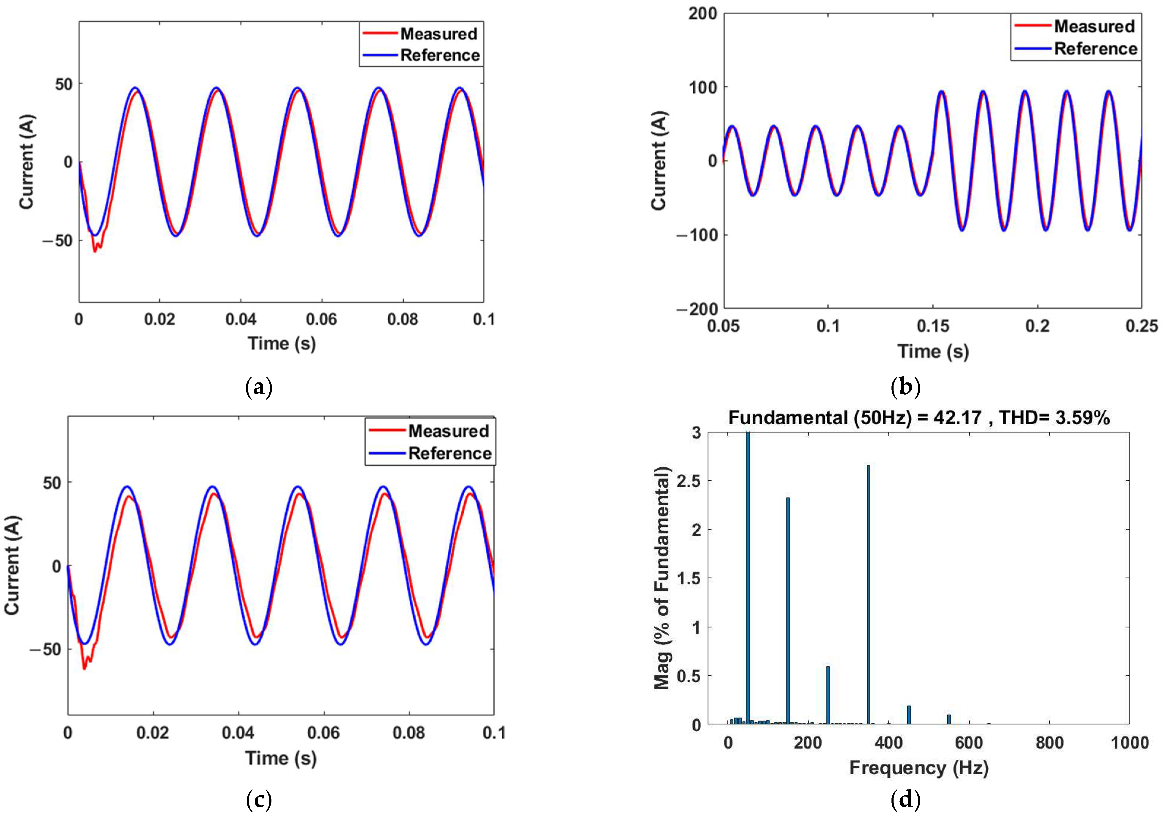
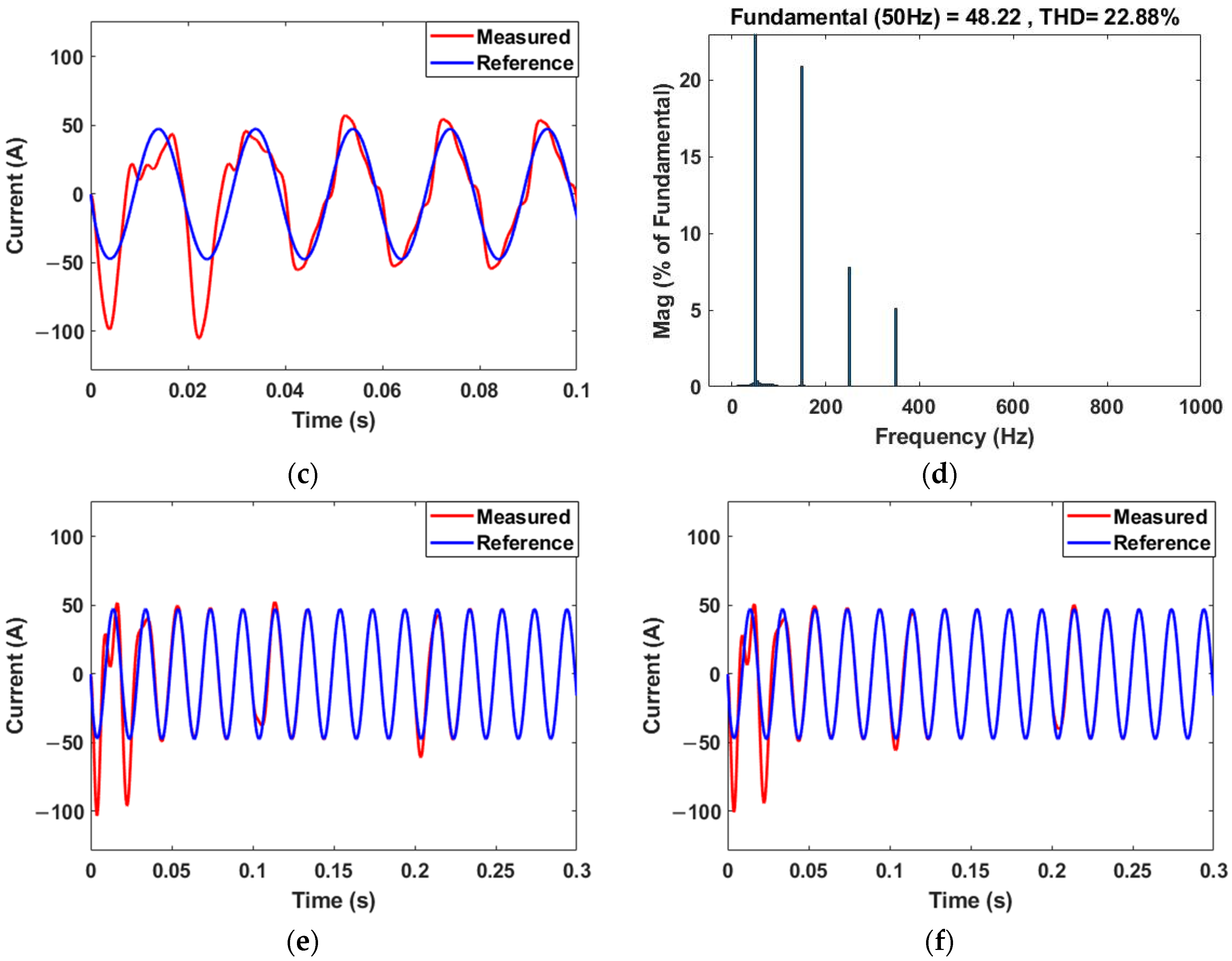
  • Under normal grid operation (NGO), the grid voltage contains no harmonics. A pure sine wave of 230 Vrms with a frequency of 50 Hz is applied at the grid terminals. Moreover, the performance is also compared when a step input from 50 A to 100 A is introduced in the reference current at 0.15 s.
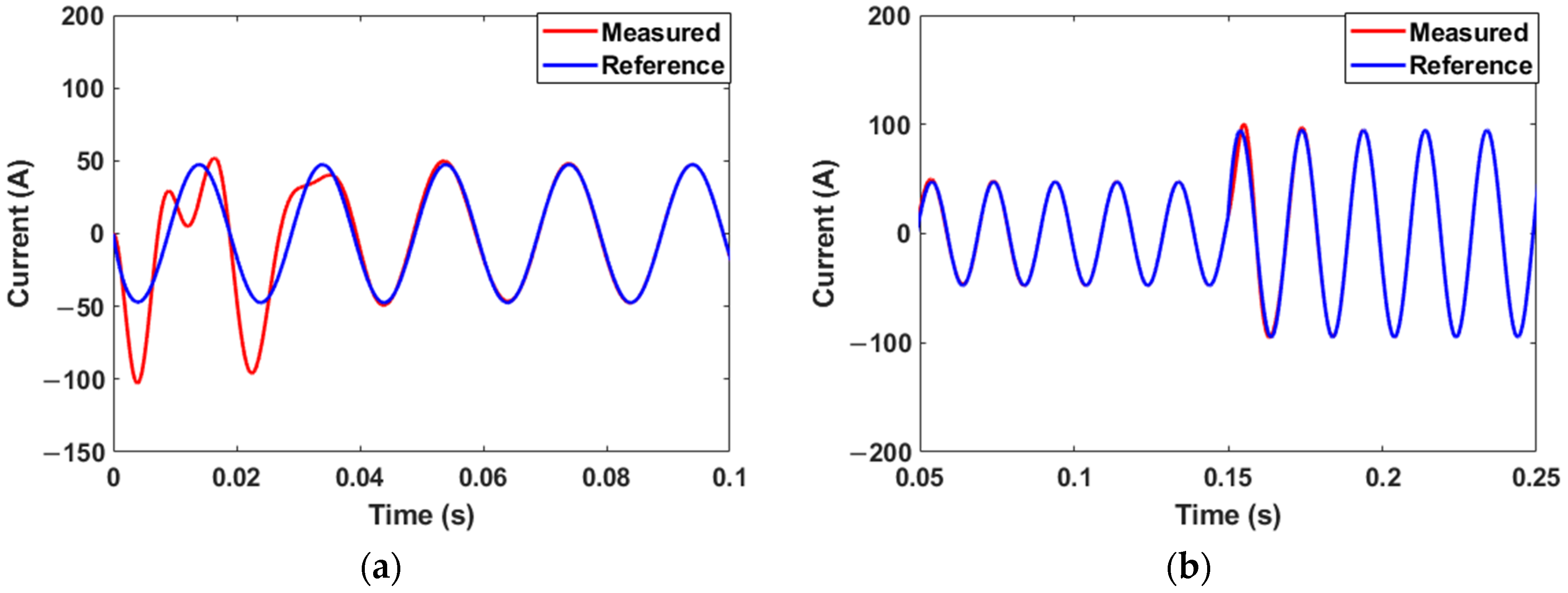
  • Inverters are assumed to be controlled as an ideal source. Perturbations present in the grid current are the result of the nonlinear loads present in the grid. Under abnormal grid operation (AGO), low-order harmonic distortions, i.e., 5% of the third, fifth and seventh harmonics, are present at grid voltages of 250 Vpeak with a nominal frequency of 50 Hz.
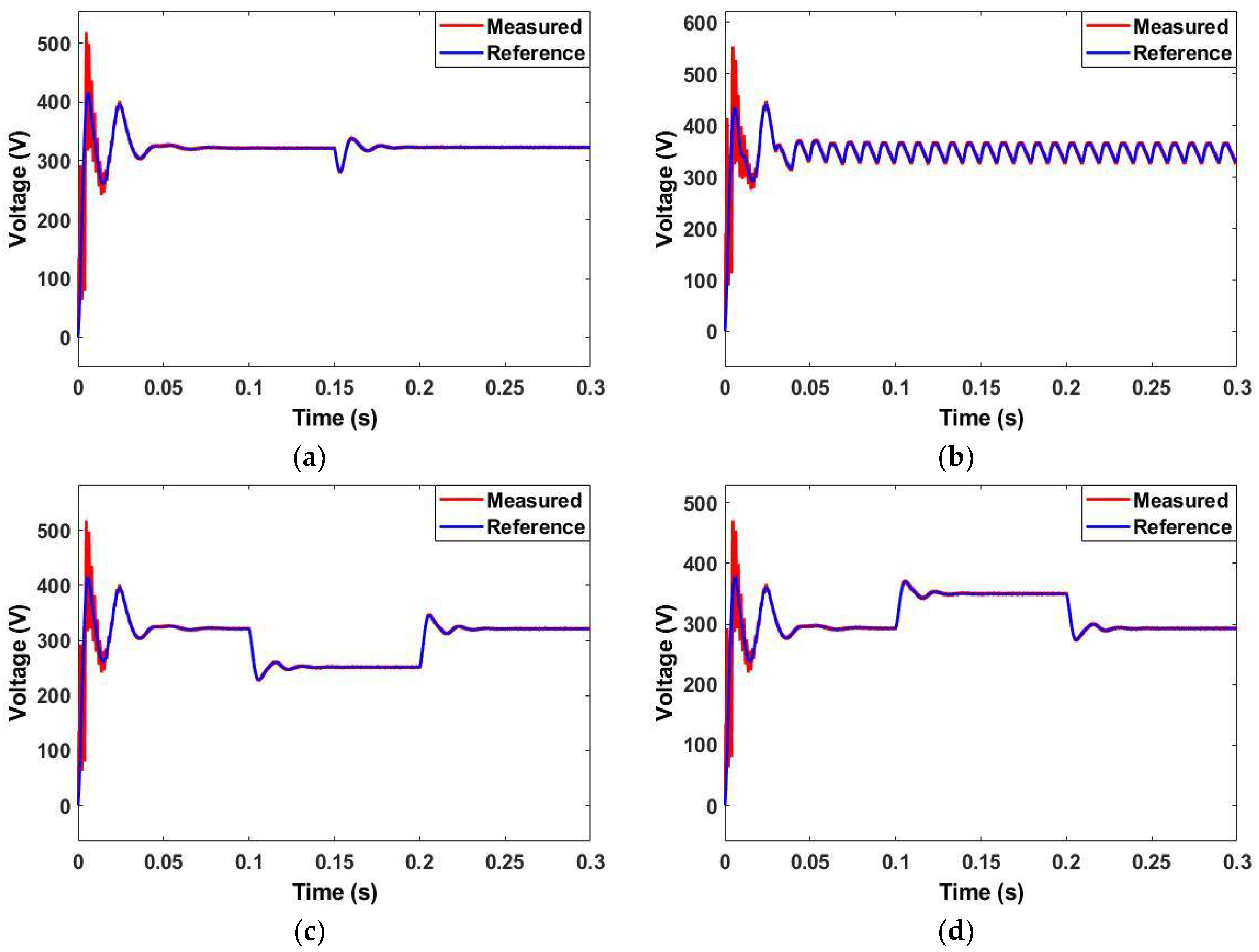
  • Under voltage sag conditions, the grid voltage drops from 230 Vrms magnitude to 180 Vrms between 0.1 s to 0.2 s. Similarly, the grid voltage rises from 210 Vrms to 250 Vrms under grid voltage swell conditions.
Figure 7 shows the response of MCAEB qZSI using the SMC-based controller under different operating conditions. Figure 7a,b show the output current I 2 under normal voltage conditions (NGO), with the step of the reference input current set at 0.15 s. By analyzing the output current response using the SMC controller, it can be observed that the rise time, percentage overshoot, settling time and THD are equal to 2.361 ms, 8.152%, 11.405 ms and 1.08%, respectively, under NGO.
Figure 7c shows the output current I 2 during AGO, and the THD is shown in Figure 7d. An increase in THD from 1.08% to 3.59% can be observed, which is below the 5% regulation under IEEE-63547. The current response during grid voltage sag and swell are shown in Figure 7e,f, respectively. Under these conditions, there is almost no change in output current when voltage sag or swell occurs at 0.1 s. This shows the robustness of the proposed controller to external disturbances.
Similarly, Figure 8 shows the DC link voltage under different operating conditions. Figure 8a–d show the DC link voltage during NGO, AGO, and voltage sag and swell in grid voltage, respectively. A rise time of 432.45 µs, 38.067% overshoot, settling time of 13.12 ms and a steady-state error of almost 1 V can be observed.
The output current of the inverter using the PI-based controller is shown in Figure 9. By analyzing these responses, it can be observed that the controller has a rise time of 4.314 ms, 29.5% overshoot, a settling time of 35–40 ms, and a THD of 1.87% and 22.88% during NGO and AGO, respectively. A slight change in output current can be observed during voltage sag and swell in grid voltages. It can be seen that the SMC controller performs better than the PI controller when disturbance in grid voltage is applied.
Similarly, the DC link voltage is shown in Figure 10 under different operating conditions, with a rise time, percentage overshoot, settling time and steady-state error of 1.632 ms, 128%, 50 ms and 1 V, respectively. Additionally, the link voltages are shown for voltage sag and swell in grid voltage in Figure 10c,d, respectively. This shows that the SMC controller for DC side performs better than the PI controller, as it has a lower rise time, overshoot percentage and settling time.

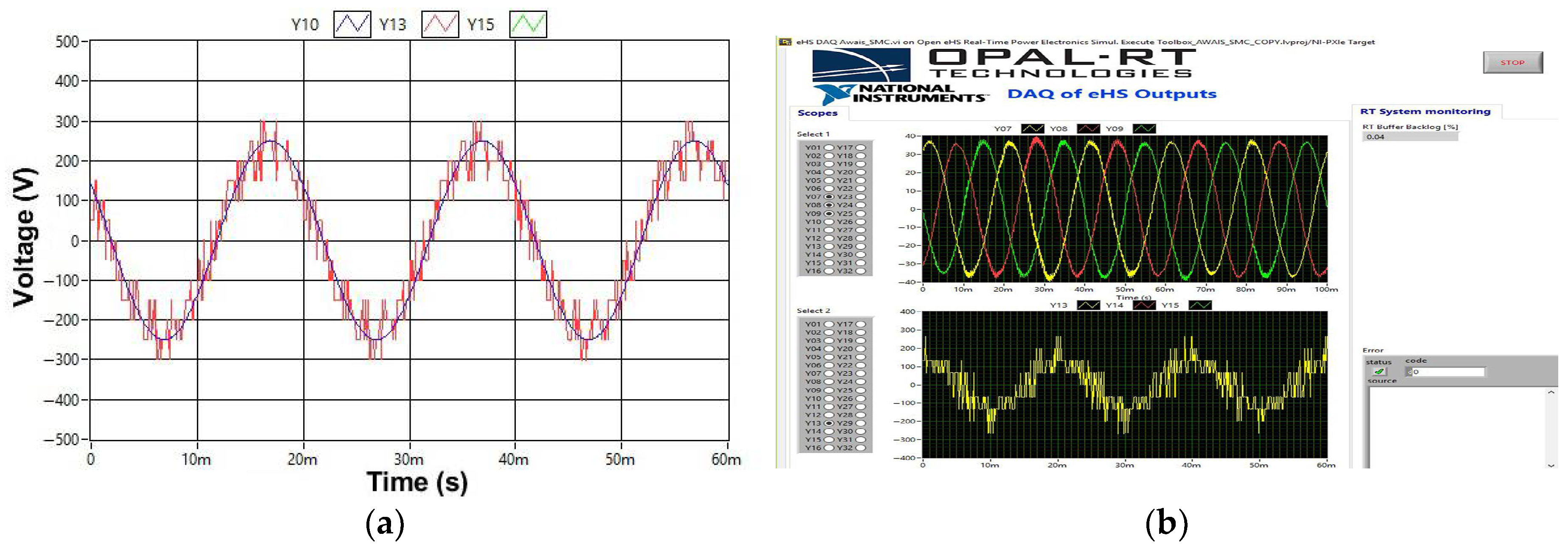
3.2. Experimental Results and Discussion

An HIL setup is established for the experimental verification of the proposed controller for the grid-tied inverter. The experimental setup consists of an OPAL-RT-based PXIe-1085 real-time power grid simulator, an NI PXIe-6738 DAQ card, an SCB-68a I/O connector, an RTA-4004 Oscilloscope and a DSPACE-1202-based Microlab-box, as shown in Figure 11. The proposed topology is simulated in real time using OPAL-RT. The SMC controller is deployed on the DSPACE-1202 using the DSPACE control Desk application. A DAQ card along with an I/O connector is used to create a feedback loop with the DSPACE.
The PXIe-1085 real-time power grid simulator is used to emulate the proposed topology at a time step of 395 ns. The open loop inverter voltage is obtained by applying the proposed SVPWM technique based on DSPACE-1202, and is shown along with the grid voltage obtained from the OPAL-RT front panel in Figure 12a. Similarly, the three-phase output current during operation of the open loop system is shown in Figure 12b. Figure 13, Figure 14 and Figure 15 show the current response of the inverter when the SMC-based closed loop controller is applied on DSPACE-1202 with a time step of 100µs.
Figure 13 and Figure 14 show the output current I 2 when reference currents of 20 A and 40 A are applied, respectively. These results show that the controller follows the reference current. Figure 15a shows the step response of single-phase current from 20 A to 40 A, while Figure 15b shows the three-phase output current obtained from the RTA-4004 oscilloscope.

4. Conclusions

This paper proposes a single-stage sliding mode control using an advanced reaching law to provide both DC link voltage and inverter control for a high-switching-frequency modified capacitor-assisted extended boost quasi-Z source multilevel inverter. An optimized topology for a multilevel three-phase inverter was selected to achieve a trade-off between switching loss and the higher number of levels. To achieve fast control, dq–gh transformation-based SVPWM was used because of its fast action, which is required at higher switching frequencies. A comparison was performed between the proposed control strategy and a PI controller on the basis of a simulation. The results of the simulation showed that the proposed controller demonstrated an extraordinary performance compared to PI-based controllers under normal and harmonic-infested grid connections. It showed strong robustness, invariance to disturbance, fast response, higher-quality current, and lower THD. Hardware-in-loop implementation was performed in Smart Grid Laboratory, and the experimental results were in agreement with the simulations, thus validating the feasibility and effectiveness of the control.

Author Contributions

Conceptualization, M.A.R. and A.U.; methodology, M.A.R. and A.U.; software, M.A.R. and A.U.; validation, M.A.R. and A.U.; formal analysis, A.K.; investigation, H.S.Z.; resources, K.Z.; data curation, A.U.; writing—original draft preparation, M.A.R.; writing—review and editing, M.A.R. and A.U.; visualization, W.U.; supervision, A.U.; project administration, A.U.; funding acquisition, W.U., A.U. and K.Z. All authors have read and agreed to the published version of the manuscript.

Funding

This research received no external funding.

Data Availability Statement

Not applicable.

Conflicts of Interest

There is no conflict of interest.

References

  1. Rahbar, K.; Chai, C.C.; Zhang, R. Energy Cooperation Optimization in Microgrids with Renewable Energy Integration. IEEE Trans. Smart Grid 2018, 9, 1482–1493. [Google Scholar] [CrossRef]
  2. Sakib, N.; Hossain, E.; Ahamed, S.I. A Qualitative Study on the United States Internet of Energy: A Step Towards Computational Sustainability. IEEE Access 2020, 8, 69003–69037. [Google Scholar] [CrossRef]
  3. Hor, C.-L.; Watson, S.J.; Majithia, S. Analyzing the impact of weather variables on monthly electricity demand. IEEE Trans. Power Syst. 2005, 20, 2078–2085. [Google Scholar] [CrossRef]
  4. An, L.; Duan, J.; Chow, M.-Y.; Duel-Hallen, A. A Distributed and Resilient Bargaining Game for Weather-Predictive Microgrid Energy Cooperation. IEEE Trans. Ind. Inform. 2019, 15, 4721–4730. [Google Scholar] [CrossRef]
  5. Dursun, M.K. LCL Filter Design for Grid Connected Three-Phase Inverter. In Proceedings of the 2nd International Symposium on Multidisciplinary Studies and Innovative Technologies (ISMSIT), Ankara, Turkey, 19–21 October 2018; pp. 1–4. [Google Scholar] [CrossRef]
  6. Mandol, M.H.; Shuvra, P.B.; Hosain, M.K.; Samad, F.; Rahman, M.W. Novel Single Phase Multilevel Inverter Topology with Reduced Number of Switching Elements and Optimum THD Performance. In Proceedings of the 2019 International Conference on Electrical, Computer and Communication Engineering (ECCE), Cox’s Bazar, Bangladesh, 7–9 February 2019; pp. 1–5. [Google Scholar] [CrossRef]
  7. Zhu, Y.; Guo, S.; Chen, L.; Yan, Q.; Ma, H.; Xie, X.; Zhang, W.; Yuan, X. A Novel Hybrid Cascaded Multilevel Inverter. In Proceedings of the 2018 IEEE International Power Electronics and Application Conference and Exposition (PEAC), Shenzhen, China, 4–7 November 2018; pp. 1–5. [Google Scholar] [CrossRef]
  8. Xu, Z.; Zheng, X.; Lin, T.; Yao, J.; Ioinovici, A. Switched-capacitor multi-level inverter with equal distribution of the capacitors discharging phases. Chin. J. Electr. Eng. 2020, 6, 42–52. [Google Scholar] [CrossRef]
  9. Peng, F.Z.; Yuan, X.; Fang, X.; Qian, Z. Z-source inverter for adjustable speed drives. IEEE Power Electron. Lett. 2003, 1, 33–35. [Google Scholar] [CrossRef]
  10. Li, T.; Cheng, Q. A comparative study of Z-source inverter and enhanced topologies. CES Trans. Electr. Mach. Syst. 2018, 2, 284–288. [Google Scholar] [CrossRef]
  11. Ho, A.-V.; Chun, T.-W. Single-Phase Modified Quasi-Z-Source Cascaded Hybrid Five-Level Inverter. IEEE Trans. Ind. Electron. 2018, 65, 5125–5134. [Google Scholar] [CrossRef]
  12. Adle, R.; Renge, M.; Muley, S.; Shobhane, P. Photovoltaic Based Series Z-source Inverter fed Induction Motor Drive with Improved Shoot through Technique. Energy Procedia 2017, 117, 329–335. [Google Scholar] [CrossRef]
  13. Ahmad, A.; Bussa, V.K.; Singh, R.K.; Mahanty, R. Switched-Boost-Modified Z-Source Inverter Topologies with Improved Voltage Gain Capability. IEEE J. Emerg. Sel. Top. Power Electron. 2018, 6, 2227–2244. [Google Scholar] [CrossRef]
  14. Hemalatha, N.; Seyezhai, R. Modified Diode Assisted Extended Boost Quasi Z-Source Inverter for PV Applications. Circuits Syst. 2016, 7, 3271–3284. [Google Scholar] [CrossRef] [Green Version]
  15. Hemalatha, N.; Ramalingam, S. Modified Capacitor Assisted Extended Boost Quasi Z-Source Inverter for The Grid-Connected PV System. IIUM Eng. J. 2019, 20, 140–157. [Google Scholar] [CrossRef]
  16. Ahmad, A.; Singh, R.K.; Beig, A.R. Switched-Capacitor Based Modified Extended High Gain Switched Boost Z-Source Inverters. IEEE Access 2019, 7, 179918–179928. [Google Scholar] [CrossRef]
  17. Jagan, V.; Kotturu, J.; Das, S. Enhanced-Boost Quasi-Z-Source Inverters with Two-Switched Impedance Networks. IEEE Trans. Ind. Electron. 2017, 64, 6885–6897. [Google Scholar] [CrossRef]
  18. Rathore, S.; Kirar, M.; Bhardwaj, S.K. Simulation of Cascaded H-Bridge Multilevel Inverter Using PD, POD, APOD Techniques. Electr. Comput. Eng. Int. J. 2015, 4, 27–41. [Google Scholar] [CrossRef]
  19. Nair, R.; Mahalakshmi, R.; Thampatty, K.C.S. Performance of three phase 11-level inverter with reduced number of switches using different PWM techniques. In Proceedings of the International Conference on Technological Advancements in Power and Energy (TAP Energy), Kollam, India, 24–26 June 2015; pp. 375–380. [Google Scholar] [CrossRef]
  20. Yan, S.; Zhang, Q.; Du, H. A simplified SVPWM control strategy for PV inverter. In Proceedings of the 24th Chinese Control and Decision Conference (CCDC), Taiyuan, China, 23–25 May 2012; pp. 225–229. [Google Scholar] [CrossRef]
  21. Jayakumar, V.; Chokkalingam, B.; Munda, J.L. A Comprehensive Review on Space Vector Modulation Techniques for Neutral Point Clamped Multi-Level Inverters. IEEE Access 2021, 9, 112104–112144. [Google Scholar] [CrossRef]
  22. Celanovic, N.; Boroyevich, D. A fast space-vector modulation algorithm for multilevel three-phase converters. IEEE Trans. Ind. Appl. 2001, 37, 637–641. [Google Scholar] [CrossRef]
  23. Khan, A.; Hu, X.M.; Khan, M.A. Real-Time Implementation and Comparative Analysis of αβ and gh Reference Framed SVPWM Techniques for a Three-Level NPC Induction Motor Drive. In Proceedings of the 2018 IEEE PES/IAS PowerAfrica, Cape Town, South Africa, 28–29 June 2018; pp. 1–6. [Google Scholar] [CrossRef]
  24. Liu, Q.; Caldognetto, T.; Buso, S. Review and Comparison of Grid-Tied Inverter Controllers in Microgrids. IEEE Trans. Power Electron. 2020, 35, 7624–7639. [Google Scholar] [CrossRef]
  25. Athari, H.; Niroomand, M.; Ataei, M. Review and Classification of Control Systems in Grid-tied Inverters. Renew. Sustain. Energy Rev. 2017, 72, 1167–1176. [Google Scholar] [CrossRef]
  26. Piao, Z.; Guo, C.; Sun, S. Adaptive Backstepping Sliding Mode Dynamic Positioning System for Pod Driven Unmanned Surface Vessel Based on Cerebellar Model Articulation Controller. IEEE Access 2020, 8, 48314–48324. [Google Scholar] [CrossRef]
  27. Xu, B.; Ran, X. Sliding Mode Control for Three-Phase Quasi-Z-Source Inverter. IEEE Access 2018, 6, 60318–60328. [Google Scholar] [CrossRef]
  28. Xiu, C.; Guo, P. Global Terminal Sliding Mode Control with the Quick Reaching Law and Its Application. IEEE Access 2018, 6, 49793–49800. [Google Scholar] [CrossRef]
Figure 1. Circuit configuration of MCAEB qZSI topology.
Energies 15 08002 g001
Figure 2. (a) Non-Shoot Through State; (b) Shoot Through State.
Energies 15 08002 g002
Figure 3. (a) dq–gh transformation; (b) projection of reference vector.
Energies 15 08002 g003
Figure 4. SVPWM strategy for qZSI Filter.
Energies 15 08002 g004
Figure 5. LCL filter single line diagram.
Energies 15 08002 g005
Figure 6. Control schematic diagram.
Energies 15 08002 g006
Figure 7. Output current I 2 using the SMC controller: (a) under NGO; (b) during step response at 0.15 s; (c) under AGO; (d) THD of AGO response; (e) during voltage sag and (f) voltage swell in grid voltage.
Energies 15 08002 g007aEnergies 15 08002 g007b
Figure 8. DC link voltage V d c using SMC controller: (a) under NGO with a step response of 0.15 s; (b) under AGO; (c) during voltage sag and (d) voltage swell in grid voltage.
Energies 15 08002 g008
Figure 9. Output current I 2 using the PI controller: (a) under NGO; (b) during step response at 0.15 s; (c) under AGO; (d) THD of AGO response; (e) during voltage sag and (f) voltage swell in grid voltage.
Energies 15 08002 g009aEnergies 15 08002 g009b
Figure 10. DC link voltage V d c using the PI controller: (a) under NGO with a step response at 0.15 s; (b) under AGO; (c) during voltage sag and (d) voltage swell in grid voltage.
Energies 15 08002 g010
Figure 11. HIL setup containing DSPACE-1202 and PXIe-1085 power grid simulator.
Energies 15 08002 g011
Figure 12. OPAL-RT front panel results: (a) single phase inverter output voltage; (b) three-phase output current with single-phase inverter output.
Energies 15 08002 g012
Figure 13. DSPACE-1202 front panel, Phase-A reference current at 20A.
Energies 15 08002 g013
Figure 14. DSPACE-1202 front panel, Phase-A reference current at 40 A.
Energies 15 08002 g014
Figure 15. Current step response from 20 A to 40 A: (a) DSPACE-1202 front panel; (b) RTA-4004 oscilloscope output.
Energies 15 08002 g015
Table 1. Design parameters for SMC and qZSI.
ParametersValues
Parameters of MCAEB qZSI, L, C 0.254 mH, 131 µF
Switching frequency of inverter, fs100 kHz
Filter parameters, L f , C f ,   L g 1.2 mH, 6 µF 1.2 mH
Sliding surface co-efficient, c 1 , c 2 , c 3 −0.0012, −0.0012, 1.117 × 10⁻⁶
Reaching law co-efficient, k 1 , k 2 ,   α 0.05, 0.002, 0.5
Sliding surface co-efficient, z 1 , z 2 , z 3 −85.8073, −0.0422, −16.707
Sliding surface co-efficient, z 4 ,   z 5 −2.0174, −84.0342
AC-side PI Gain, k p 1 , k i 1 −0.29837, −706.5122
DC-side PI Gain, k p 2 ,   k i 2 −0.346536, −289.5905
Publisher’s Note: MDPI stays neutral with regard to jurisdictional claims in published maps and institutional affiliations.

