Article

Development and Control of a Switched Capacitor Multilevel Inverter

1
Department of Electrical Engineering, ZHCET, Aligarh Muslim University, Aligarh 202002, India
2
Department of Electrical and Computer Engineering, Florida International University, Miami, FL 33174, USA
3
Industrial Engineering Department, College of Engineering, King Saud University, Riyadh 11421, Saudi Arabia
*
Author to whom correspondence should be addressed.
Energies 2023, 16(11), 4269; https://doi.org/10.3390/en16114269
Submission received: 15 March 2023 / Revised: 21 April 2023 / Accepted: 6 May 2023 / Published: 23 May 2023

Abstract

:
This article offers a novel boost inverter construction with a Nine-level quadruple voltage boosting waveform. The primary drawback of conventional MLI is the need for a high voltage DC-DC converter to increase the voltage when using renewable energy sources. Consequently, the developed method, complete with a quadruple voltage boost ability, can alleviate that shortcoming by automatically increased the incoming voltage. A single DC source, two switching capacitors, and eleven switches are all that are used in the newly presented architecture. The voltage of the capacitor automatically balances. The switched capacitor MLI is distinguished by the fewer parts that are required and the substitution of a capacitor for a DC source. The switching capacitor has to be charged and discharged properly in order to produce the nine-level output voltage waveform. The SPSC unit makes these levels attainable. To achieve voltage boosting, switched capacitors are coupled in parallel and series in the conduction channel. The quality of this proposed topology has been analyzed through different parameters based on the components count, THD, and cost; the resulting efficiency reaches 97.85%. The switching order of the proposed method has been controlled by the Nearest Level Modulation Method (NLC). MATLAB and PLECS software were used to evaluate the constructed Nine-level converter.

1. Introduction

Multilevel inverters have revolutionized the power electronics industry by providing an effective solution to voltage issues encountered in high-power applications. The need for high voltage has always been a challenge, and multilevel inverters have brought a significant change to the traditional approach of generating high-voltage waveforms [1]. The primary objective of multilevel inverters is to generate output voltages that are higher than the input voltage levels by using multiple levels of DC sources. These inverters are gaining increasing popularity in the industrial and commercial sectors, and their application is expanding rapidly [2].
The concept of multilevel inverters was first proposed in the 1970s. Since then, it has been a topic of extensive research and development. Today, multilevel inverters are widespread in in various high-power utilization, including solar power s, electric vehicles, and industrial drives [3]. Multilevel inverter technology has proven to be a reliable and cost-effective solution for generating excellent outcomes. waveforms with low harmonic distortion. The development of multilevel inverter technology has been driven by the increasing demand for high-voltage applications that require low distortion levels [4]. The conventional two-level inverter was the standard solution for low-power applications, but it has its limitations when it comes to high-voltage applications. The two-level inverter generates square wave outputs that are rich in harmonic distortion, resulting in high losses and reduced efficiency. The multilevel inverter, on the other hand, offers a solution to this problem by producing output waveforms with low harmonic distortion; this results in high efficiency and reduced lossesMultilevel inverters work by combining many levels of DC sources to get the correct output voltage waveform [5]. The diode-clamped inverter, the flying capacitor inverter, and the cascaded H-bridge inverter (CHB) are the three topologies for multilevel inverters that are most often used. These topologies vary in terms of the amount of DC sources used as well as the control method [6]. While the flying capacitor inverter employs capacitors to store energy and balance the voltage levels, the diode-clamped inverter uses multiple diodes to clamp the output voltage. The CHB inverter uses multiple H-bridge modules, each with its DC source, to generate the desired output waveform [7,8,9,10,11].
Multilevel inverters offer several benefits over traditional 2-level inverters. These advantages include minimized harmonic distortion, improved efficiency, increased reliability, and reduced stress on the power electronics components [12]. Multilevel inverters also offer improved voltage and current waveforms, which result in reduced electromagnetic interference and reduced acoustic noise. Multilevel inverter technology has gained significant attention in the renewable energy sector, where the need for high-voltage, low-distortion waveforms is crucial [2,13]. the use of multilevel inverters in wind and solar power resources and other renewable energy systems has been shown to increase the power conversion process’s dependability and efficiency. The use of multilevel inverters in electric vehicles has also been shown to enhance the efficiency of the mechanism for converting energy, resulting in increased range and reduced charging times [14]. A switched capacitor multilevel inverter (SCMLI) is an emerging power electronics device that converts DC voltage into multiple levels of AC voltage. It is composed of a series of switched capacitor cells that are used to create multiple output voltage levels. Compared to conventional 2-level inverters, this technology provides a number of benefits, notably lower switching losses, less harmonic distortion, and better output waveform quality [15,16]. The capacity of an SCMLI to produce high-quality output waveforms is one of its main advantages. The inverter may do this by employing a variety of voltage levels, which allows it to simulate a sinusoidal waveform. This results in reduced harmonic distortion, which is a major concern in many applications, such as motor control and renewable energy systems. Additionally, the output voltage can be finely controlled by adjusting the duty cycle of the switching signals, allowing for precise control over the load.
Another advantage of an SCMLI is its ability to operate at higher switching frequencies. Because the output voltage is generated using multiple levels, the switching frequency can be increased without the need for higher voltage switching devices. This reduces switching losses and improves overall efficiency [17]. Additionally, because the output voltage is generated using capacitors, there is no need for large inductors, which can be bulky and expensive.
One of the main challenges with SCMLI technology is the need for careful capacitor balancing. Because each cell in the inverter requires a different capacitor value, it is important must make sure that each capacitor’s voltage is balanced [18,19,20]. This can be achieved using a variety of balancing techniques, such as charge redistribution or voltage clamping. Additionally, because the capacitors must be charged and discharged in sequence, the inverter must be carefully designed to ensure that the switching signals are synchronized. Another challenge with SCMLI technology is the complexity of the control circuitry. Because the inverter requires precise control over the switching signals and capacitor voltages, a complex control circuit is required. This can be challenging to design and implement, particularly in high-power applications. Despite these challenges, SCMLI technology has several promising applications. One potential application is in renewable energy systems, where high-quality AC waveforms are required to interface with the grid. Additionally, SCMLI technology can be used in motor control applications, where precise control over the output voltage is critical. The technology is also well-suited for high-power applications, where the benefits of reduced switching losses and improved efficiency are particularly valuable. In summary, switched capacitor multilevel inverters are a promising technology for power electronics applications. They offer several advantages over traditional two-level inverters, including improved waveform quality, reduced harmonic distortion, and higher switching frequencies [19,20]. However, careful capacitor balancing and complex control circuitry are required, making the technology challenging to design and implement. Despite these challenges, SCMLI technology has several promising applications, particularly in alternative energy sources, motor control, and effective applications. As a result, researchers now shift towards the switched capacitor multilevel [20].
The format of this paper is as follows: details on the recommended topology and modulation strategy are provided in Section 2. In Section 3, a thorough comparison of several SC-based MLI configuration is given. In Section 4 and Section 5, respectively, the study of power loss and various simulation output results for various loads are presented. Section 6 explains the experimental behavior of the presented topology. Section 7 goes into further detail about this paper’s conclusion.

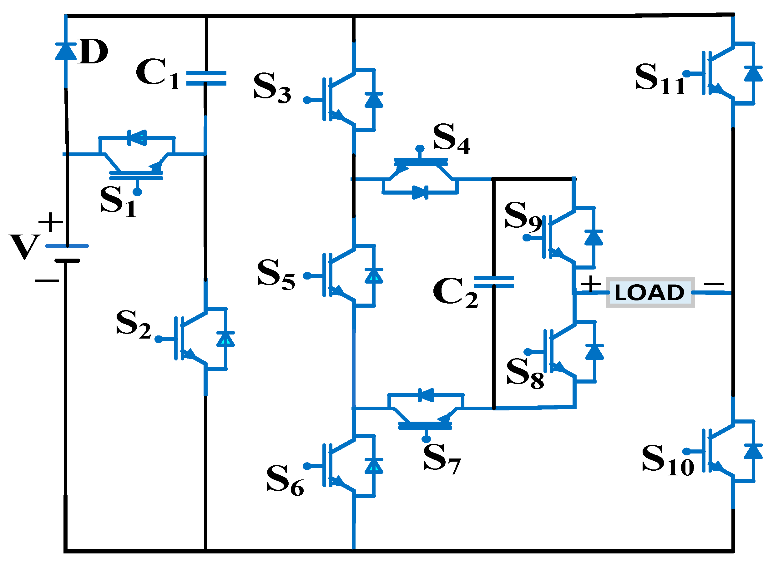
2. Specifics of Proposed Topology

2.1. Configuration of Proposed Topology

Figure 1 shows the module for the newly developed quadruple Nine-level voltage boost inverter. One DC source, two switched capacitors (C1 and C2), eleven power electronic switches ( S 1 to S 11 ), and a power diode (D) make up the newly presented circuit. Only one DC source is used to create The nine levels of the generated voltage waveform. The source charges the switched capacitor in parallel at first, then the switched capacitor in series at a later stage. The nine-level output is produced by adding the output voltage. The suggested topology’s switching states for producing the nine-level output voltage are shown in Table 1. ON state of switch is indicated by 1 and OFF state is indicated by 0.
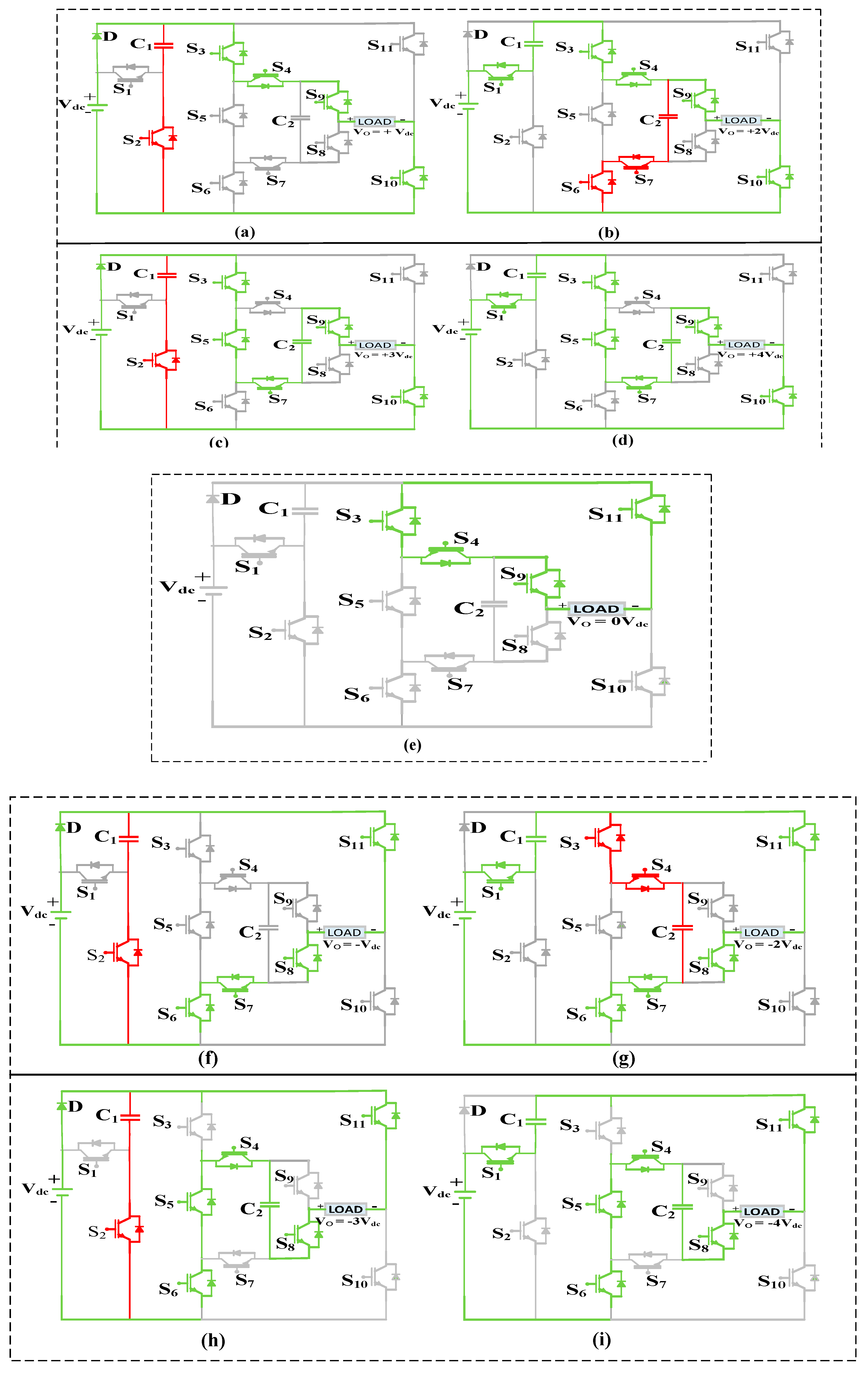
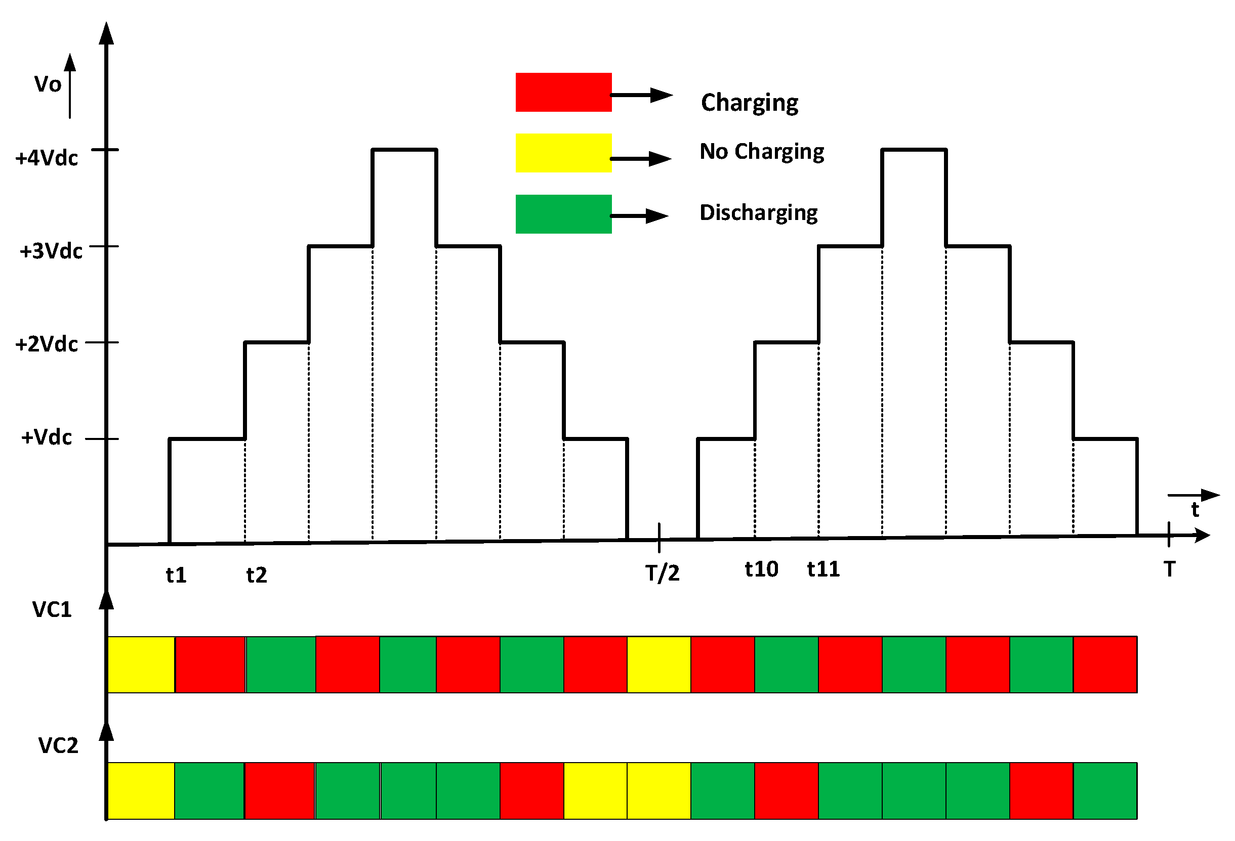
  • Level 1: +Vdc output level is produced in this mode. S 3 ,  S 4 , S 9 , and S 10 switches are in the ON state in Figure 2a, while every other switch are in the OFF state. Powered by stored energy in C1, switch S 2 is ON.
  • Level 2: In this mode, an output level of +2 Vdc is produced. The S 1 , S 3 , S 4 , S 9 , and S 10 switches are ON, while all other switches are OFF, as illustrated in Figure 2b. As the voltage source and capacitors C1 and C2 become parallel, switches S 6 and S 7 are turned ON to access the energy storage in C2. There is a 2 Vdc charge on the capacitor C2. The voltage source provides the load with the necessary energy via the capacitor C1 in series.
  • Level 3: The output level of this mode is +3 Vdc. As seen in Figure 2c, the S 3 , S 5 , S 7 , S 9 , and S 10 switches are ON while the other switches are OFF. By switching S 2 , the C1’s accumulated energy is turned on. The DC input source is linked in parallel with C1’s capacitor. The load receives the required amount of energy from the voltage source linked in series with C2.
  • Level 4: An output level of +4 Vdc is the result. With the exception of the S 1   S 3 , S 5 , S 7 , S 9 , and S 10 switches, all other switches are in the OFF state. The load is now connected in series with the capacitors C2, C1, and the SC source, as indicated in Figure 2d, providing the load with the energy it needs.
  • Level 5: The output level of this mode is 0 Vdc. As shown in Figure 2e, all switches in this configuration, with the exception of S 3 , S 4 , S 9 , and S 11 , are in the off position. The voltage across the load is 0 volts because there isn’t a DC supply.
  • Level 6: The output level of this mode is −Vdc. As seen in Figure 2f, the switches S 6 , S 7 , S 8 , and S 11 are ON while the other switches are OFF. Switch S 2 is ON and powered by energy stored in C1.
  • Level 7: The mode’s level of output is −2 Vdc. As seen in Figure 2g, only the S 1 , S 6 , S 7 , S 8 , and S 11 switches are active while every other switch is off. Switches S 3 and S 4 are switched ON to access the capacitor C2’s stored energy when it enters parallel with the voltage source and capacitor C1. The capacitor C2 is charged to a voltage of 2 Vdc. The energy for the load is given by the voltage source coupled in series with a capacitor.
  • Level 8: This mode produces an output level of −3 Vdc. The S 4 , S 5 , S 6 , S 9 , and S 11 switches are ON, while all other switches are OFF, as illustrated in Figure 2h. The stored energy in C1 is activated via switch S 2 . The DC input source is linked in parallel with the C1 capacitor. The load is powered by the voltage source connected in series with C2.
  • Level 9: The output level of this mode is −4 Vdc. With the exception of the S 1 , S 4 , S 5 , S 6 , S 8 , and S 11 switches, all other switches are in the OFF state. To provide the load with the energy it requires, the capacitors C2, C1, and the DC source are linked in series with the load. Figure 2i depicts the current trend.

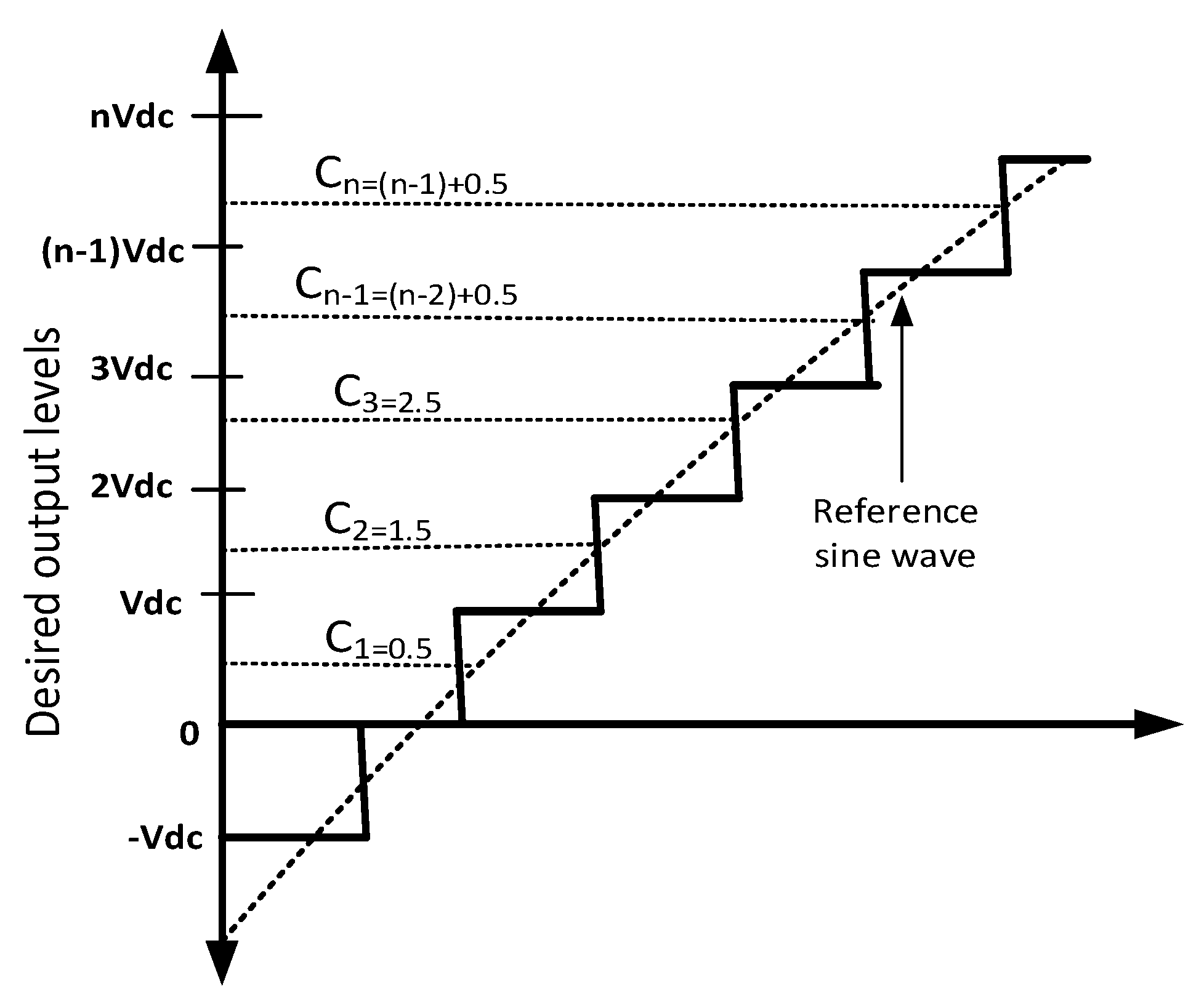
2.2. Nearest Level Control

Modulation technique plays an important role in multilevel inverters. It affects the harmonics, switching losses, and filter size [15]. The output voltage is controlled using the modulation approach, which also enhances the harmonic profile. Based on the level of frequency, the modulation technique can be broadly classified into two categories. For a high-frequency scheme—Phase shift Pulse width modulation (PSPWM) and level shift pulse width modulation are used. The triangular carrier waves in the PSPWM scheme have the same frequency but are not in phase (adjacent carrier).
To generate N-voltage levels, (N − 1) triangular carriers are required. The shifted carrier waves are spaced apart by (360/N − 1). To create the gate control signals, the modulating signal and carrier wave are compared. [20]. For lower level frequency—selective harmonic elimination (SHE) and nearest level control (NLC) are used [1]. In this paper, the nearest modulation method has been preferred. NLC is preferred for high-power applications. As NLC works on a fundamental frequency, switching losses get decreased; in addition, the implementation of NLC is simple [3]. In selective harmonic elimination, there are many transcendental equations that are not easy to solve because of their complex nature. As such, this problem associated with the SHE scheme has been resolved by the NLC modulation method [8].
Signal switching for the proposed SCMLI has been generated by the NLC modulation method. When the reference signal crosses the constant signal, the switching state shifts to the next higher level. The reference sinusoidal signal in NLC is compared with the multiple constant signals, which differ in amplitude by unity. The functioning of the NLC is shown in Figure 3. The modulation index can be defined by,
M o d u l a t i o n   i n d e x = o u t p u t   r m s   v o l t a g e I n p u t   D C   v o l t a g e < 1

3. Comparative Analysis

The broad range of capabilities of the designed boost inverter topology have been demonstrated by a comparative analysis with a few selected topologies. The comparison is based on the topologies’ switch counts, diode counts, capacitor counts, and voltage boosts. All topologies with a unity source and Nine-level output voltage are included in the comparison. Based on boosting settings and component counts, Table 2 provides a comparison. The topology in [12] consists of more capacitors and diodes when compared to other topologies mentioned in the table below. As the components increase, its TSV increases and ultimately cost increases also. The topology depicted in [14] has a TSV approximation. It is near the proposed topology but has more switches and one extra capacitor. An important performance factor (cost factor) is defined by
C.F = Nsw + Nd + Nc + α(TSV)
= 11 + 1 + 1 + 2 + 0.5(5) = 17.5
Nsw = number of switches, Nd = number of the diode, Nc = number of the capacitor, α = cost function (constant) can be taken as 0.5, TSV = Total standing voltage, C.F = Cost factor
This can be used to display the inverter’s entire cost. The efficiency and cost factor depending on how many components are used. Therefore, our proposed topology has higher efficiency and a lower cost factor.
This section shows a comparison based on the quantity of switches required to provide nine levels in various topologies. The introduced topology has reduced switch count-based MLI. Figure 4a shows that the introduced SCMLI configuration uses a lower number of power semiconductor switches when contrast to further configuration used as a basis for comparison. The greater the number of switches, the greater the switching and conduction losses. This will automatically influence the efficiency of the configuration. Figure 4b depicts the efficiency (97% approx.) compared to alternative topologies.

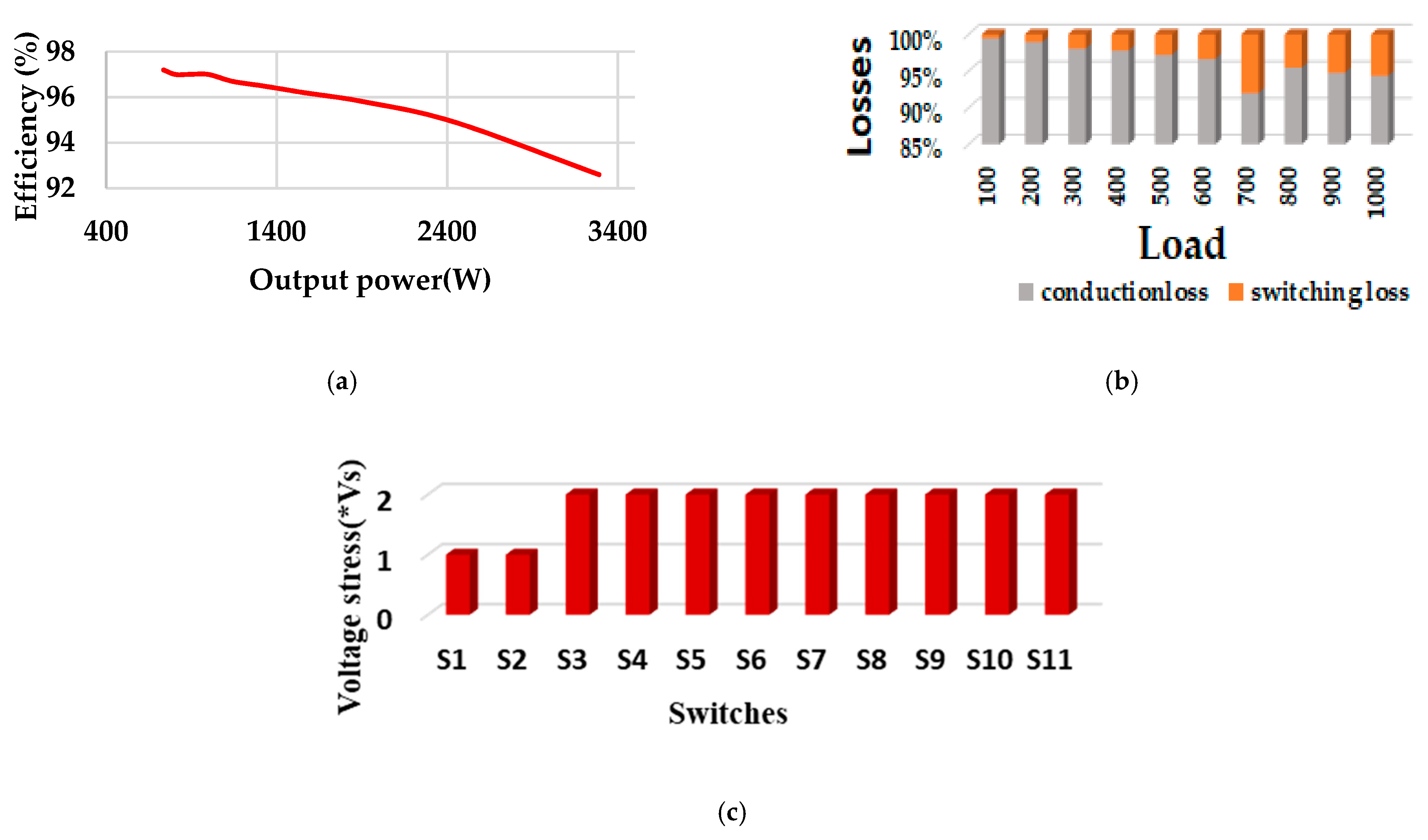
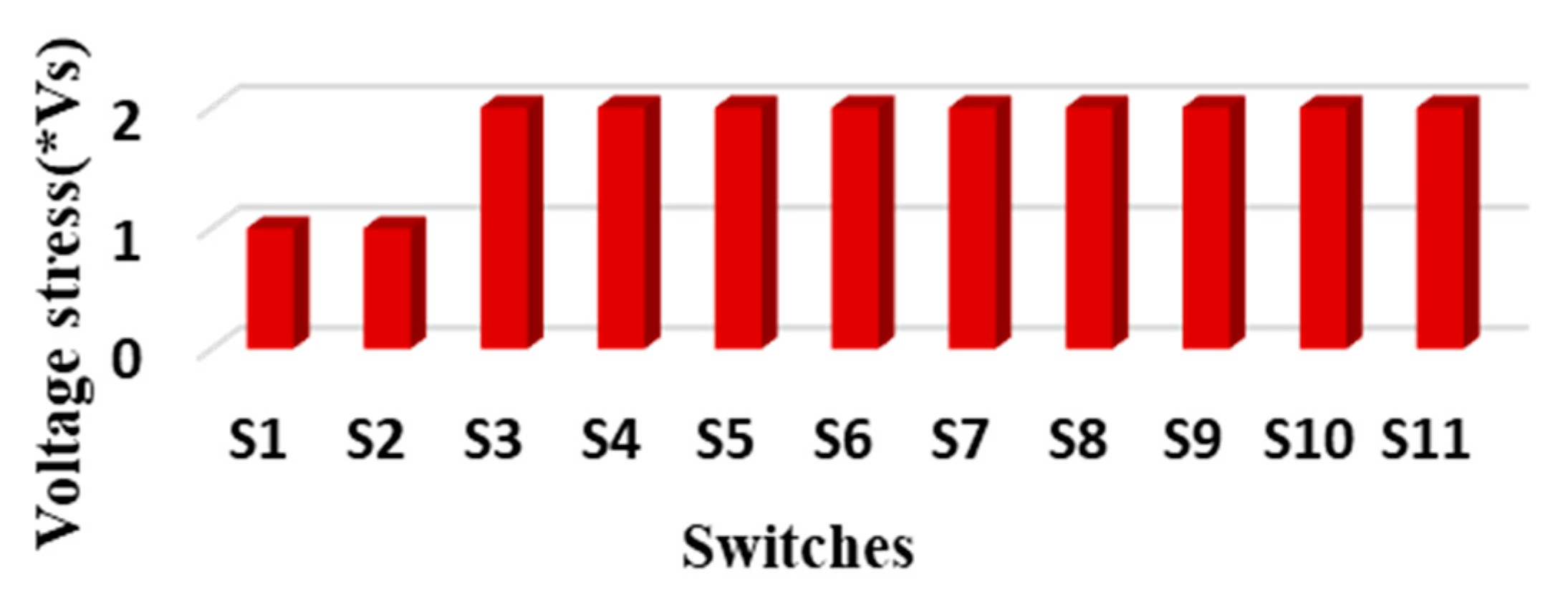
4. Power Loss Analysis

The conduction losses and switching losses are added to determine the prototype’s overall power loss. This section uses the fundamental switching frequency to determine the conduction losses and switching losses of the recommended SCMLI module. The losses of each element of the suggested topology were calculated using the PLECS software. Several loads have been used to estimate the power loss.

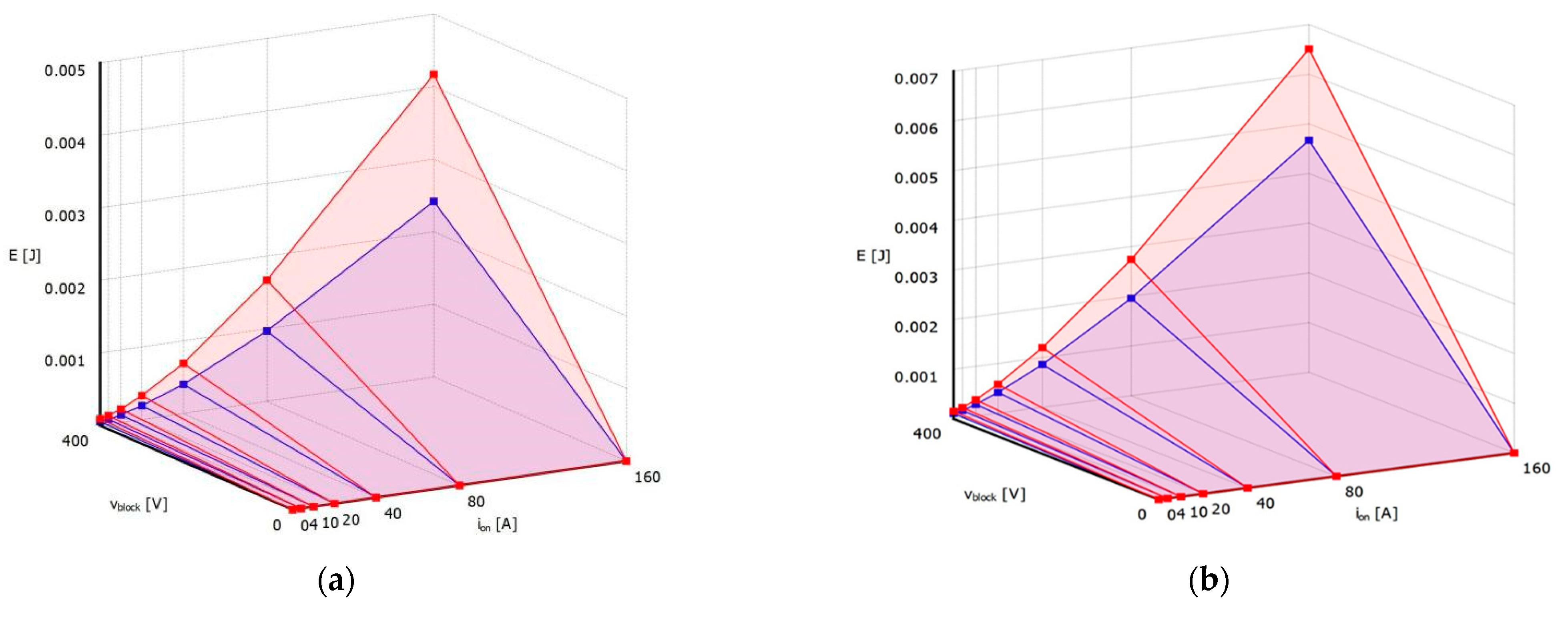
4.1. A-Switching Losses

Switching loss took place during the ON (1) and OFF (0) stages of switching states. For the purpose of simplicity, switch voltage and current are considered to be linear throughout the switching time. The following equations may be presented for the power switch in question using this assumption as a foundation.
P o n = f s w 0 t o n V s ,   i s ( t )   i ( t )       = 1 / 6   f s w   V s ,   I i   t o n P o f f = f s w 0 t o f f V s , i s ( t )   i = 1 / 6   f s w   V s ,   I i   t off
where the switching frequency is fsw, The power switch’s currents in the ON and OFF states are Iiand Ii′, respectively, and Vs and Vsw are the voltages in the nth power switch’s OFF state. To calculate the total switching loss, multiply the sum of the ON Son and OFF Soff switching states per cycle provided in the calculation below.
P s l = N = 1 11 ( n = 1 S o n P o n , i n     n = 1 S o f f P o f f , i n

4.2. B-Conduction Loss

The conduction loss can be calculated directly by:
P conduction ( sw ) = i = 1 11 ( V on   ( sw ) × i avg ( sw ) + R on   ( sw ) × i 2 rms ) P conduction ( D ) = N = 1 11 ( V on   ( D ) × i avg ( D ) + R on   ( D ) × i 2 rms )
where the on-state voltages of the Nth switch and diode, respectively, are Von (sw) and Von (D). Ron (sw) and Ron (D), respectively, reflect the Nth switch’s internal on-state resistance.
In PLECS software, the thermal modelling of the designed topology has been examined. Figure 5a–c, which illustrate the conduction loss for the Infineon IGBT switch 1KW25N120H3 up to 20A, and thermal modelling of the turn ON and OFF switch, respectively. For various loads, the power loss has been examined in PLECS.

4.3. Capacitor Selection

Half of the output voltage waveform is divided into eight time steps. Furthermore, switching happens at a fundamental frequency. What follows is a formula for calculating the time steps t1, t2, and t3.
t 1 = sin 1 V d c 4 V d c w ,   t 2 = sin 1 2 V d c 4 V d c w ,   t 3 = sin 1 3 V d c 4 V d c w
As observed in Figure 6, the longest discharge interval for C1 is from the interval t2 to t3. The charge discharged during this interval is given by:
Q 1 = t 2 t 3 i L d t C 1 2 V I N R V C t 3 t 2
On similar basis C2 is calculated and is given by Equation (1).
C 2 2 V I N R V C t 3 t 2
where VIN = input dc voltage, VC = voltage across capacitor, and R = Resistive load.
Figure 7a describes the efficiency and the output power in watts for resistive load (100 Ω). For resistive load =1 KΩ, the achieved maximum efficiency is 97.85%. Figure 7b shows the conduction and switching loss vs load across each switch of the proposed topology. As the load increases, the conduction losses decrease.

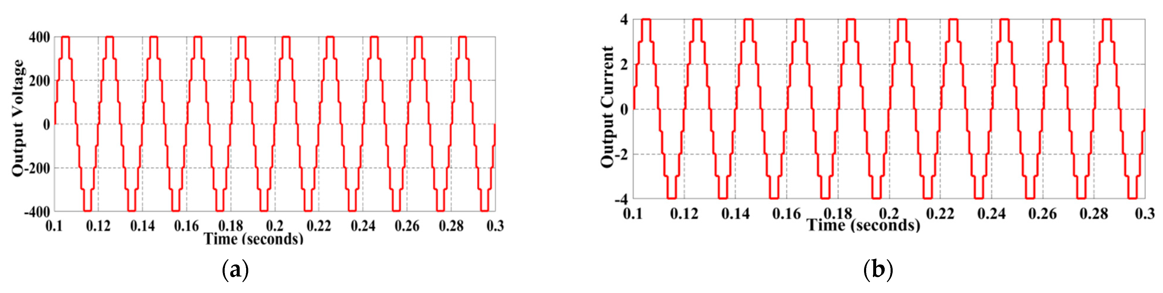
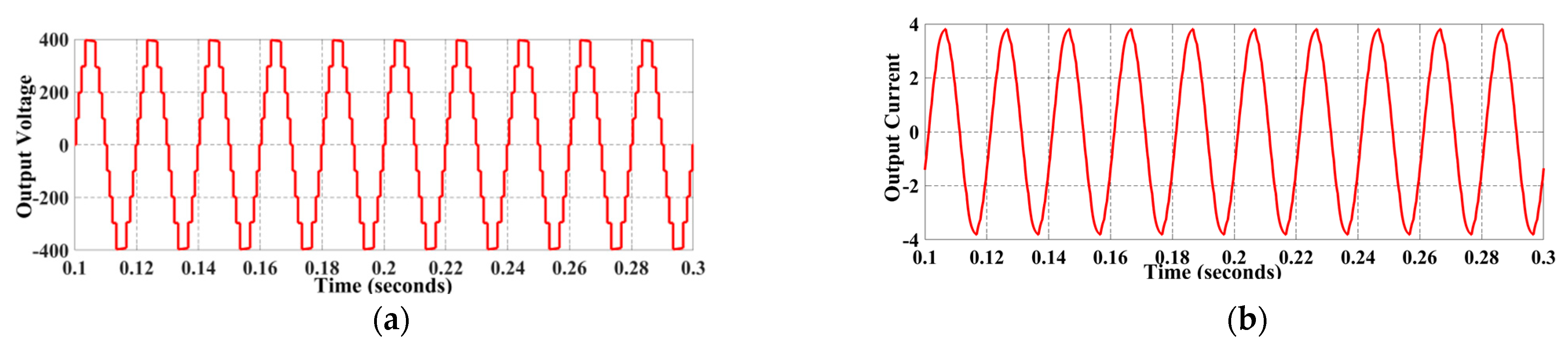
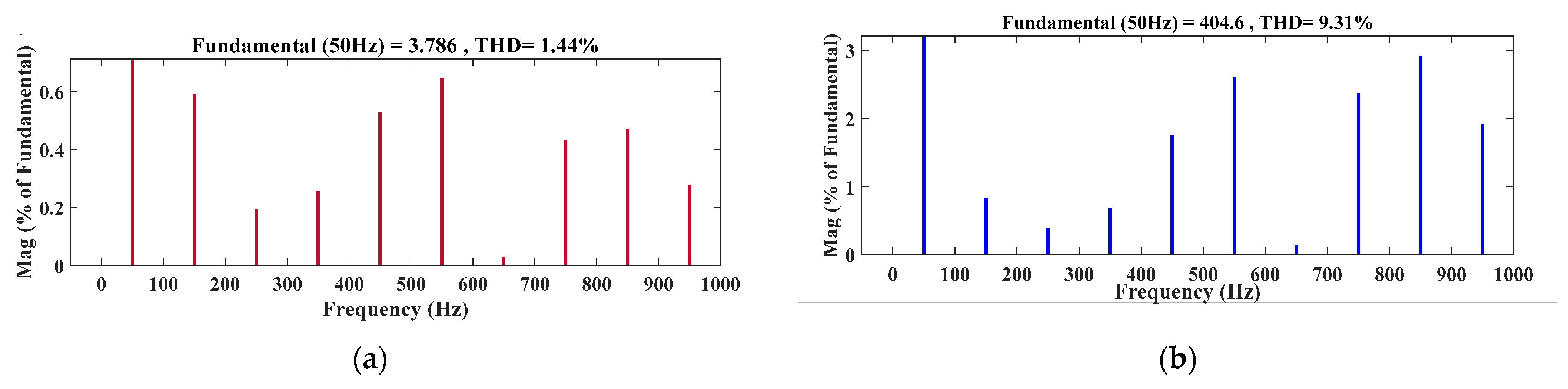
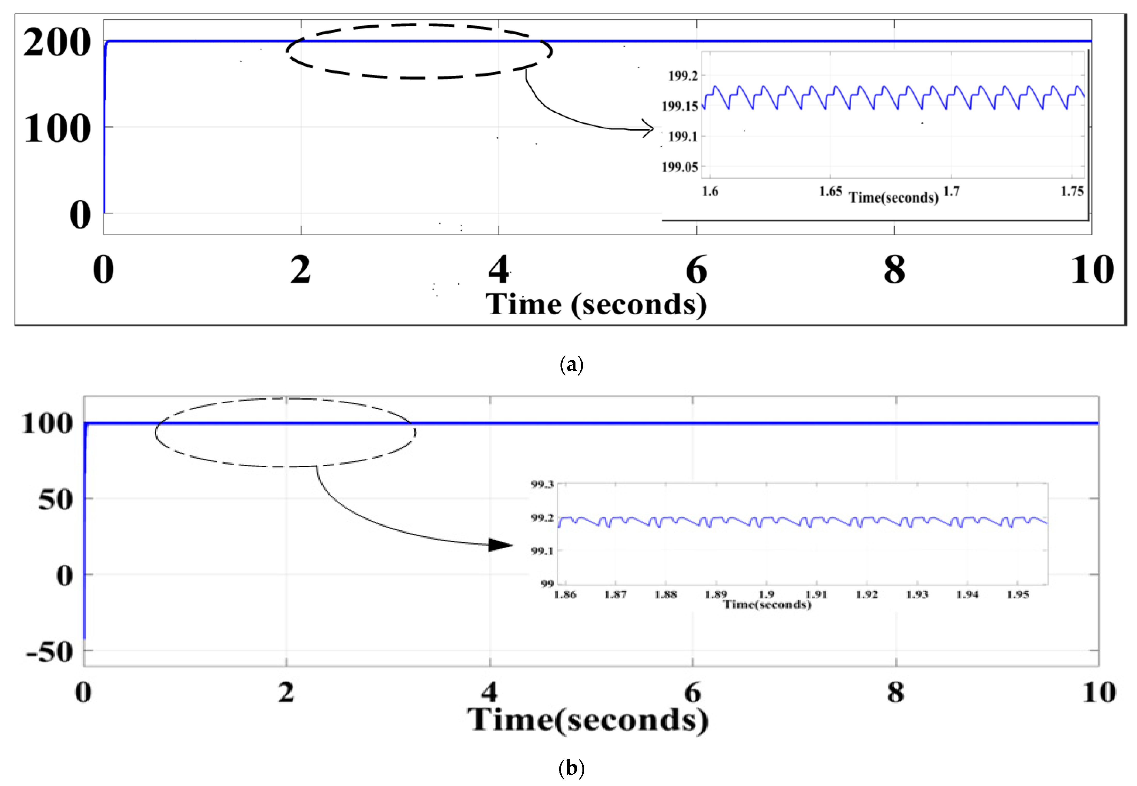
5. Result and Discussion

Simulation Result

MATLAB software was used to run the simulation in order to verify the MLI structure’s functionality. The parameters used for the simulation are displayed in Table 3 below. In order to generate gate pulses, the NLC method is used.
Figure 8 and Figure 9, shows the recommended architecture’s output voltage, output current. According to the output voltage waveform, the input voltage Vs is increased to levels 2 Vs, 3 Vs, and 4 Vs, creating the nine levels in the output voltage. Figure 8a,b display the output voltage and current at R = 100 ohm. The voltage and current for the RL load (R = 100 + 120 mH) are shown in Figure 9a,b. Figure 10b demonstrates that the output voltage THD under RL load (R = 100 + 120 mH) is 9.31% and the output current THD is 1.44%. Stress across each switch is depicted in Figure 11. Capacitor voltages Vc1 and Vc2, respectively is shown in Figure 12. This figure also shows that the voltage in between the capacitor may be preserved consistency at 100 V and 200 V (500 + 360 mH) without the need of any control devices. When the load switches from being just resistive to becoming RL load, there is an increase in the ripples but voltage across the capacitor remains balanced. Although there would be fluctuation in Vc1 and Vc2 during charging and discharging, the change is insignificant. Moreover, balancing has been ensured by parallel charging of the capacitor through the DC source and discharge through load. This demonstrates how capacitor voltage may be balanced on its own without the use of a control mechanism. Table 4 provides an explanation of the simulation results that validate the suggested topology’s ability to produce the 9-level output voltage.

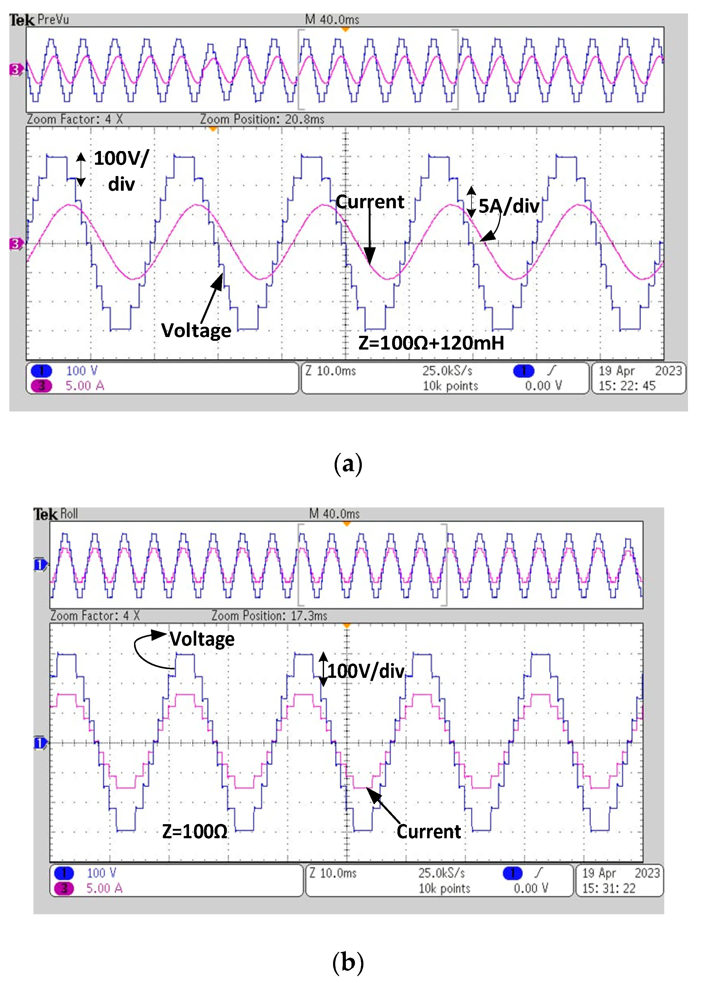
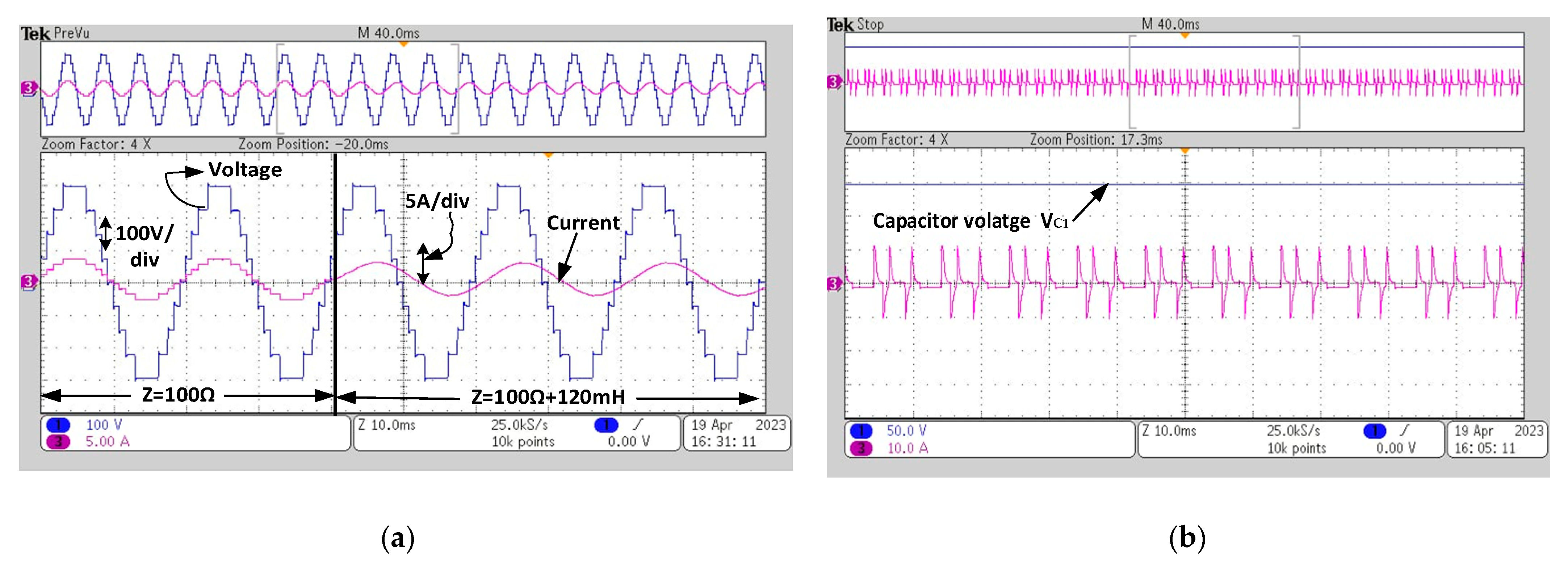
6. Experiment Result

As seen in Figure 13, the hardware prototype was developed to execute the experimental findings in order to validate the simulation findings. A nine-level output voltage has been produced using the NLC modulation approach and the fundamental switching frequency. A 75-volt DC input powers the prototype’s nine levels of output. The gate pulse is produced by the microcontroller TMS320F28379D for various switches. The gate driver circuit for these IGBTs is created using a TLP 250 integrated circuit. The output voltage and current waveform with a resistive load (100) are shown in Figure 14b. Figure 14a displays the experimental results for a number of connected resistive and inductive loads with Z = 100 + 120 mH. Figure 15a shows the voltage and current waveforms for dynamic load changes from an inductive load to a totally resistive load, and Figure 15b shows the capacitor voltage across C1. All of these experimental findings demonstrate that the proposed topology operates satisfactorily across capacitors without the need for any extra control methods.

7. Conclusions

This project introduces a unique boost inverter with built-in subconscious equalization capabilities. FCs have the same charging and discharging times, hence less capacitance is needed. Fewer switches with built-in polarity generators showed the advantages of the configuration mode, which has lower power losses and is more efficient for medium voltage applications. A notable drawback of traditional multilevel inverters is the requirement for high voltage DC-DC power converters for voltage increase when employing renewable energy sources like photovoltaic and fuel cell technologies. As a result, the recommended architecture’s triple voltage boost feature solves that issue by automatically raising the input voltage. MATLAB and PLECS software is used to simulate-verify the developed 9-level converter.

Author Contributions

Conceptualization, S.M., A.S. and M.T.; Formal analysis, S.M.; Investigation, S.M., S.A. and H.A.M.; Methodology, S.M., A.S. and M.T.; Supervision, A.S. and M.T.; Validation, S.M., A.S. and M.T.; Writing—original draft, S.M., A.S. and M.T.; Writing—review & editing, S.A. and H.A.M. All authors have read and agreed to the published version of the manuscript.

Funding

This research has received funding from King Saud University through Researchers Supporting Project number (RSP2023R387), King Saud University, Riyadh, Saudi Arabia.

Data Availability Statement

Not applicable.

Acknowledgments

The authors extend their appreciation to King Saud University for funding this work through Researchers Supporting Project number (RSP2023R387), King Saud University, Riyadh, Saudi Arabia.

Conflicts of Interest

The authors declare no conflict of interest.

References

  1. Emadi, A.; Williamson, S.S.; Khaligh, A. Power electronics intensive solutions for advanced electric, hybrid electric, and fuel cell vehicular power systems. IEEE Trans. Power Electron. 2006, 21, 567–577. [Google Scholar] [CrossRef]
  2. Jahan, H.K.; Abapour, M.; Zare, K. Switched-capacitor-based single-source cascaded H-bridge multilevel inverter featuring boosting ability. IEEE Trans. Power Electron. 2019, 34, 1113–1124. [Google Scholar] [CrossRef]
  3. Kumari, M.; Siddique, M.D.; Sarwar, A.; Mekhilef, S.; Tariq, M. A twice boost nine-level switched-capacitor multilevel (2B-9L-SCMLI) inverter with self-voltage balancing capability. Int. J. Circuit Theory Appl. 2021, 49, 2578–2592. [Google Scholar] [CrossRef]
  4. Khoun-Jahan, H.; Shotorbani, A.M.; Abapour, M.; Zare, K.; Hosseini, S.H.; Blaabjerg, F.; Yang, Y. Switched capacitor based cascaded half-bridge multilevel inverter with voltage boosting feature. In CPSS Transactions on Power Electronics and Applications; CPSS: Shenzhen, China, 2021; Volume 6, pp. 63–73. [Google Scholar] [CrossRef]
  5. Panda, K.P.; Babu, N.; Bisoyi, S.K.; Panda, G. Reduced Switch Quadruple Boost Switched-Capacitor based Multilevel Inverter. In Proceedings of the 2020 3rd International Conference on Energy, Power and Environment: Towards Clean Energy Technologies, Shillong, India, 5–7 March 2021; pp. 1–6. [Google Scholar] [CrossRef]
  6. Chakraborty, C.; Iu, H.H.C.; Lu, D.D.C. Power converters, control, and energy management for distributed generation. IEEE Trans. Ind. Electron. 2015, 62, 4466–4470. [Google Scholar] [CrossRef]
  7. Hussan, M.R.; Sarwar, A.; Khan, I.; Tariq, M.; Tayyab, M.; Alhosaini, W. An eleven-level switched-capacitor inverter with boosting capability. Electronics 2021, 10, 2262. [Google Scholar] [CrossRef]
  8. Siddique, M.D.; Mekhilef, S.; Shah, N.M.; Sarwar, A.; Iqbal, A.; Tayyab, M.; Ansari, M.K. Low switching frequency based asymmetrical multilevel inverter topology with reduced switch count. IEEE Access 2019, 7, 86374–86383. [Google Scholar] [CrossRef]
  9. Barzegarkhoo, R.; Moradzadeh, M.; Blaabjerg, F. A new boost switched-capacitor multilevel converter with reduced circuit devices. IEEE Trans. Power Electron. 2018, 33, 6738–6754. [Google Scholar] [CrossRef]
  10. Hinago, Y.; Koizumi, H. A switched-capacitor inverter using series/parallel conversion with inductive load. IEEE Trans. Ind. Electron. 2012, 59, 878–887. [Google Scholar] [CrossRef]
  11. Taghvaie, A.; Adabi, J.; Rezanejad, M. A self-balanced step-up multilevel inverter based on switched capacitor structure. IEEE Trans. Power Electron. 2018, 33, 199–209. [Google Scholar] [CrossRef]
  12. Barzegarkhoo, R.; Lee, S.S.; Khan, S.A.; Siwakoti, Y.; Lu, D.D.-C. A novel generalized common-ground switched-capacitor multilevel inverter suitable for transformerless grid-connected applications. IEEE Trans. Power Electron. 2021, 36, 10293–10306. [Google Scholar] [CrossRef]
  13. Dhara, S.; Somasekhar, V.T. A nine-level transformerless boost inverter with leakage current reduction and fractional direct power transfer capability for PV applications. IEEE J. Emerg. Sel. Top. Power Electron. 2021, 10, 7938–7949. [Google Scholar] [CrossRef]
  14. Jakkula, S.; Jayaram, N.; Pulavarthi, S.V.K.; Shankar, Y.R.; Rajesh, J. A Generalized High Gain Multilevel Inverter for Small Scale Solar Photovoltaic Applications. IEEE Access 2022, 10, 25175–25189. [Google Scholar] [CrossRef]
  15. Wu, D.; Peng, L. Characteristics of nearest level modulation method with circulating current control for modular multilevel converter. IET Power Electron. 2016, 9, 155–164. [Google Scholar] [CrossRef]
  16. Zhang, Y.; Li, L. A step-up switched capacitor multilevel inverter with reduced switches tolerating lower stress. In Proceedings of the 2020 15th IEEE Conference on Industrial Electronics and Applications (ICIEA), Kristiansand, Norway, 9–13 November 2020; pp. 811–816. [Google Scholar] [CrossRef]
  17. Thota, P.R.; Jeevananthan, S. A New Switched Capacitor Nine-Level Inverter with Quadruple Voltage Boosting and Capacitor Voltage Balancing Capabilities. In Proceedings of the 2020 IEEE International Conference on Power Electronics, Drives and Energy Systems (PEDES), Jaipur, India, 16–19 December 2020; pp. 1–5. [Google Scholar] [CrossRef]
  18. Siddique, M.D.; Iqbal, A.; Riyaz, A. Single-Phase 9L Switched-Capacitor Boost Multilevel Inverter (9L-SC-BMLI) Topology. In Proceedings of the 2020 IEEE International Conference on Power Electronics, Drives and Energy Systems (PEDES), Jaipur, India, 23 September 2022; pp. 1–5. [Google Scholar] [CrossRef]
  19. Siddique, M.D.; Mekhilef, S.; Shah, N.M.; Ali, J.S.M.; Meraj, M.; Iqbal, A.; Al-Hitmi, M.A. A New Single Phase Single Switched-Capacitor Based Nine-Level Boost Inverter Topology with Reduced Switch Count and Voltage Stress. IEEE Access 2019, 7, 174178–174188. [Google Scholar] [CrossRef]
  20. Sarwar, M.I.; Sarwar, A.; Farooqui, S.A.; Tariq, M.; Fahad, M.; Beig, A.R.; Alamr, B. A Hybrid Nearest Level Combined with PWM Control Strategy: Analysis and Implementation on Cascaded H-Bridge Multilevel Inverter and its Fault Tolerant Topology. IEEE Access 2021, 9, 44266–44282. [Google Scholar] [CrossRef]
Figure 1. Circuit diagram of the introduced topology.
Energies 16 04269 g001
Figure 2. Switching states (a) VO = +Vdc (b) VO = + 2 Vdc (c) VO = +3 Vdc (d) VO = +4 Vdc (e) VO = 0 Vdc. (f) VO = −Vdc (g) VO = −2 Vdc (h) VO = −3 Vdc (i) VO = −4 Vdc.
Energies 16 04269 g002
Figure 3. Implementation of nearest level control.
Energies 16 04269 g003
Figure 4. Comparison of proposed topology on the basis of (a) number of switches (b) topology efficiency [10,11,12,13,14,15].
Energies 16 04269 g004
Figure 5. Losses for (a) turn ON losses, (b) turn OFF losses, and (c) conduction losses for IGBT IKW25N120H3 up to 20A [Von = on state voltage drop (V), Ion = ON state current (A), Vblock = OFF state blocking voltage (V), E = Energy loss (J)].
Energies 16 04269 g005aEnergies 16 04269 g005b
Figure 6. Charging and discharging states of Capacitor C1 and C2.
Energies 16 04269 g006
Figure 7. (a) switching loss vs conduction loss vs load, (b) Efficiency (%) vs output power (watt) curve, (c) voltage stress across each switch.
Energies 16 04269 g007
Figure 8. Waveform of (a) output voltage and (b) output current with Resistive load (R = 100 Ω).
Energies 16 04269 g008
Figure 9. Waveform of (a) Load output voltage and (b) Load output current with inductive load of (Z = 100 Ω + 120 mH).
Energies 16 04269 g009
Figure 10. (a,b) THD of output voltage and current on RL Load (R = 100, L = 120 mH).
Energies 16 04269 g010
Figure 11. Voltage stress across each switch.
Energies 16 04269 g011
Figure 12. (a) Voltage across C1 = 100 V (b) C2 = 200 V at Z = 500 Ω + 360 mH.
Energies 16 04269 g012
Figure 13. Experimental setup.
Energies 16 04269 g013
Figure 14. Experimental results with NLC-PWM (a) Output voltage and current waveform with Z = 100 Ω + 120 mH and (b) output voltage and current with Z = 100 Ω.
Energies 16 04269 g014
Figure 15. (a) Output voltage and current waveform with change of load from Z = 100 Ω to Z = 100 Ω + 120 mH (b) voltage waveform across capacitor C1.
Energies 16 04269 g015
Table 1. Inverter Topology Switching States.
LevelsS1S2S3S4S5S6S7S8S9S10S11C1C2
+Vdc01110000110C-
+2 Vdc10110110110DC
+3 Vdc01101010110CD
+4 Vdc10101010110DD
0 Vdc00110000101--
−Vdc01000111001C-
−2 Vdc10110111001DC
−3 Vdc01011101001CD
−4 Vdc10011101001DD
Where C = Charging state, D = Discharging state.
Table 2. Detailed comparison of the proposed topology with different nine-level topologies.
Ref.NNswNdNcTSVGainC.F
[10]9101226224
[11]913036.25430.56
[12]919334.75445.18
[13]914046422
[14]912247.5322.75
[15]915046422
[P]911125417.5
N = number of levels, Nsw = number of switches, Nd = number of the diode, Nc = number of the capacitor. TSV-Total standing voltage, C.F—cost factor
Table 3. Parameters used for MATLAB simulation.
ParameterValues
Input voltage source100 V
Resistive Load100 ohm, 500 ohm
Capacitors (C1 = C2)4600 µF
Inductive Load120 mH, 360 mH
Input & output frequency50 Hz, 50 Hz
Table 4. MATLAB simulation output result.
Peak output voltage400 V
Peak output current3.786 A
TSV(p.u)5
Cost Factor(C.F)17.5
Disclaimer/Publisher’s Note: The statements, opinions and data contained in all publications are solely those of the individual author(s) and contributor(s) and not of MDPI and/or the editor(s). MDPI and/or the editor(s) disclaim responsibility for any injury to people or property resulting from any ideas, methods, instructions or products referred to in the content.

