Abstract
Molybdenum disulfide (MoS2) has attracted great attention from researchers because of its large band gap, good mechanical toughness and stable physical properties; it has become the ideal material for the next-generation optoelectronic devices. However, the large Schottky barrier height (ΦB) and contact resistance are obstacles hampering the fabrication of high-power MoS2 transistors. The electronic transport characteristics of MoS2 transistors with two different contact structures are investigated in detail, including a copper (Cu) metal–MoS2 channel and copper (Cu) metal–TiO2-MoS2 channel. Contact optimization is conducted by adjusting the thickness of the TiO2 interlayer between the metal and MoS2. The metal-interlayer-semiconductor (MIS) structure with a 1.5 nm thick TiO2 layer has a smaller Schottky barrier of 22 meV. The results provide insights into the engineering of MIS contacts and interfaces to improve transistor characteristics.
1. Introduction
Two-dimensional (2D) layered materials have special properties, such as atomic-level thickness and a lack of dangling bonds on the surface. Therefore, nanodevices based on two-dimensional materials possess excellent electrical properties, such as high electron mobility and high on-off ratios. Hence, two-dimensional materials show unique application prospects in electronic devices [1,2,3,4,5,6,7]. Among the various 2D materials, graphene exhibits extraordinary linear dispersion for charge carriers and possesses other unique physical properties due to the ultra-thin atomic layer thickness [8,9]. The conduction and valence bands of graphene are symmetrical about the Dirac point and its energy bandgap is almost zero; this makes it difficult for graphene-based field effect transistors (FETs) to show the on-off state in devices.
Molybdenum disulfide is a typical multi-layer transition metal chalcogenide, which is composed of sulfur–molybdenum atoms bound by covalent bonds and stacked vertically in layers. The layers interact with each other through weak van der Waals forces. Compared with graphene, molybdenum disulfide is a widely used 2D material with a bandgap of 1.8 eV for the monolayer structure and 1.2 eV for the bulk materials [10,11]. The bandgap of molybdenum sulfide increases with a decreasing number of layers, and the FET based on molybdenum disulfide may be more suitable for logic circuits. Theoretically, FETs based on MoS2 have superior room-temperature carrier mobility (410 cm2 V−1 s−1) [12] and a high on/off ratio (>108) [13]. However, MoS2 FETs with these excellent characteristics have yet to be realized by experiments. One key factor affecting the low carrier mobility is the metal–MoS2 contact and interface. Fermi level pinning leads to a large barrier height at the metal–MoS2 contact, consequently increasing the contact resistance (Rc) at the interface [14]. Metal electrodes with different work functions have been used to improve the contact; however, when molybdenum disulfide is in contact with the metal electrode, the pinning effect of the Fermi surface changes the effects and the contact metal is very weak. Various ways to reduce the contact resistance of MoS2 FETs have been reported. For example, H. Du et al. constructed MoS2–graphene heterojunction FETs using single/bi-layer graphene as contact electrodes to improve the contact interface [15]. Compared to the bilayer graphene electrode, the device has better electron transport properties and higher mobility due to the better gate control capability of the single layer graphene. However, it requires the use of complex transfer techniques and is not conducive to large-scale production. Y. Du et al. prepared polyethyleneimine-doped MoS2 FETs with reduced contact resistance and improved field-effect mobility [16]. Owing to the strong electronic doping of polyethyleneimine molecules, the mobility increases from 20.4 to 32.7 cm2 V−1 s−1. The low-work-function metal (scandium) has also been used as the contact metal to improve the contact in MoS2 FETs to obtain a higher carrier injection [17]. The device with a scandium contact has a small Schottky barrier height of 30 eV and high mobility of 184 cm2 V−1 s−1. However, the poor cyclic stability of chemical doping plagues the formation of stable contacts. Low-work-function metals are easily oxidized in air, thereby limiting commercial adoption. Recently, inserting a Fermi level unpinning layer between MoS2 and metal electrodes to construct a MIS structure was suggested to reduce ΦB. For example, an ultrathin interlayer, such as Ta2O5 or h-BN, was proposed to reduce ΦB and Rc [18,19]. Y. Kim et al. fabricated Ti-TiO2 interlayer–MoS2 channel FETs by the atomic layer deposition of 2.7 nm TiO2 to reduce the noise amplitude and contact resistance [20]. Although efforts have been made to eliminate Fermi level pinning, there have been few studies on the relationship between Fermi level unpinning and device performance.
In this work, we systematically study the above issues by modulating the thicknesses (0, 1, 1.5 and 2.2 nm) of the TiO2 interfacial layer. The barrier height and contact resistance of different TiO2 intercalation thicknesses are studied in detail. After inserting a 1.5 nm thick TiO2 layer into the meta–MoS2 interface, the MIS structure shows a reduced ΦB of 22 meV and an Rc of 4 kΩ·µm. The electron mobility is also derived for different TiO2 intercalation thicknesses. The mobility is closely related to the contact interface between the metal and MoS2, and the intrinsic mobility is easily masked by the Schottky barrier at the contact interface. As a result of the improved interface, the MoS2–TiO2 FET shows the highest field-effect mobility of 58 cm2 V−1 s−1. The barrier height and contact resistance can be controlled by the TiO2 thickness; thus, this provides insights into the design of MIS FETs.
2. Experimental Samples and Analysis Techniques
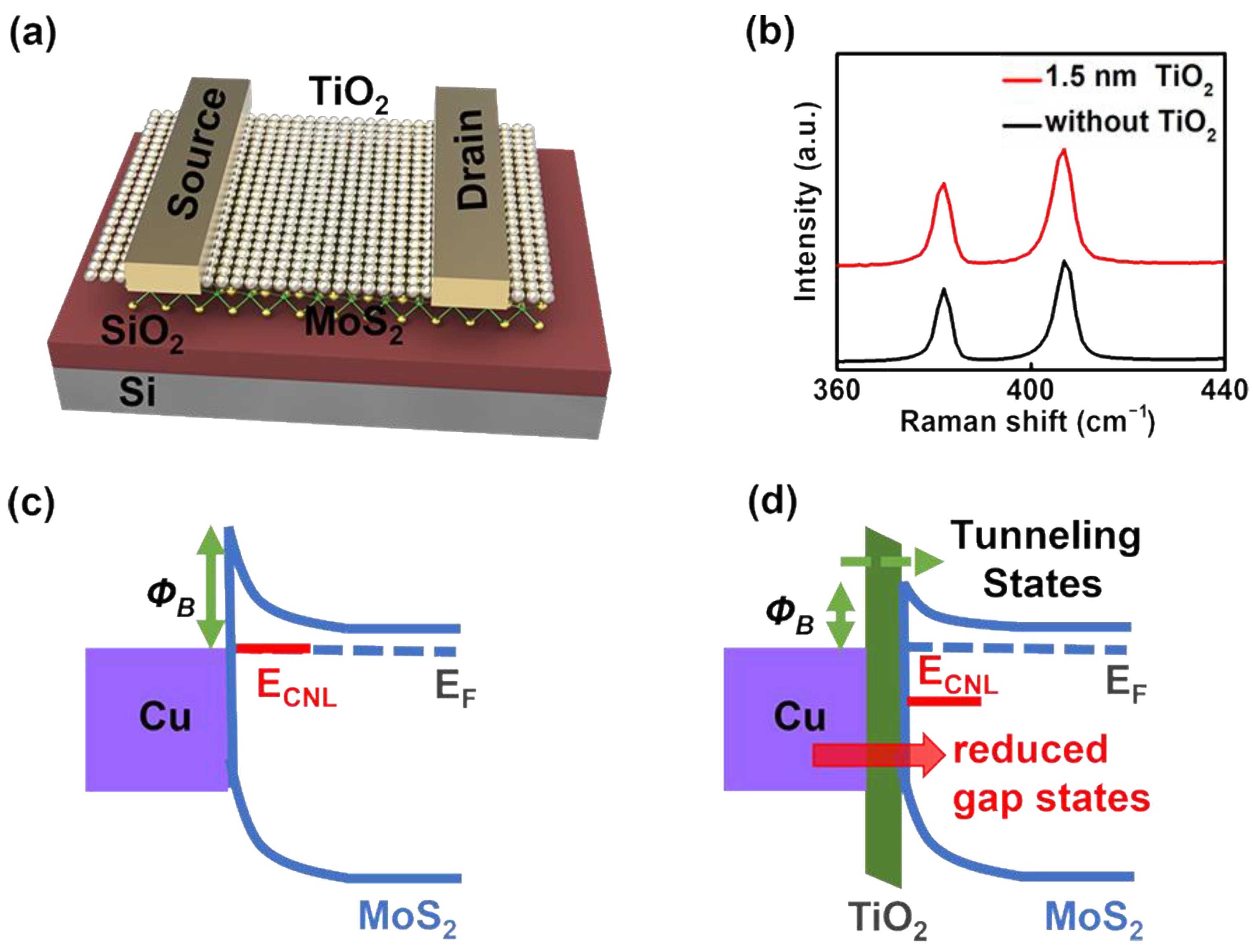
Device Fabrication and Measurements: The multilayer MoS2 flakes were exfoliated onto the SiO2/Si substrate (300 nm thick SiO2). Ti layers with various thicknesses of 0.2–1 nm were deposited on the MoS2 surface by electron beam evaporation; and vaporizing the low melting point metal for re-oxidation, thus avoiding damage of the surface of the materials. The devices were dried in an oven for two days. As shown in Figure 1, the TiO2 layers after oxidation were analyzed by atomic force microscopy (AFM); moreover, the TiO2 thicknesses were determined to be 1, 1.5, 1.8, 2.2 and 2.5 nm. Methyl methacrylate (MMA) and polymethyl methacrylate (PMMA) were spin-coated on the substrate; electron beam lithography (JEOL 6510 with NPGS) was used to define the source/drain patterns. The source and drain electrodes (15/50 nm thick Cu/Au film) were formed by thermal vaporizer deposition. Acetone was used in the lift-off process to form the electrodes. Electrical characterization was conducted on the Lake Shore TTPX Probe Station and Agilent 4155C Semiconductor Parameter Analyzer in vacuum.
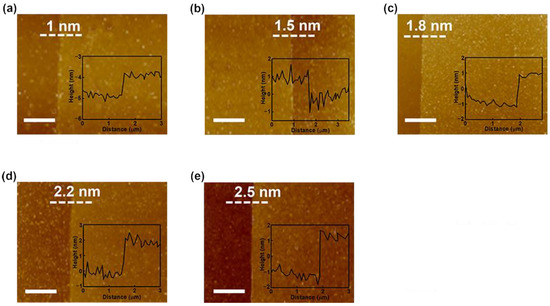
Figure 1.
(a–e) AFM images of the TiO2 interlayers with different thicknesses on the SiO2 substrate. The thicknesses of Ti are 0.2, 0.4, 0.6, 0.8 and 1 nm; these correspond to thicknesses of TiO2 of 1, 1.5, 1.8, 2.2 and 2.5 nm, respectively. The scale bar is 2 µm.
Characterization: The TiO2 thickness was determined by AFM (Bruker Multimode 8) and the XPS spectra were acquired on the Thermo Fisher ESCALAB 250Xi system (Thermo Fisher Scientific, Waltham, MA, USA) with an Al Kα X-ray source. The MoS2 flakes were analyzed by Raman scattering (RENISHAW Invia) with a 532 nm laser under ambient conditions.
3. Results and Discussion
Figure 2a displays the schematic of the MoS2 FETs with a TiO2 layer between the metal electrode and MoS2 contact. Figure 3a shows the Ti 2p XPS spectra of TiO2 with different thicknesses. The peaks at 458.5 eV and 464.2 eV are consistent with Ti 2p1/2 and Ti 2p3/2, respectively; with the latter being associated with Ti4+ [21]. When the thickness of Ti is 3 nm, the sample is not fully oxidized and the peak shows an obvious left shift; this means that part of Ti4+ is reduced to a low-valence Tix+ species [22]. Therefore, it is important to vaporize a suitable metal thickness to obtain a high-quality interfacial layer. The Raman spectra do not change significantly after coverage with a TiO2 layer (Figure 2b), indicating marginal lattice damage during deposition of the low melting point metal. Figure 2c,d show the band diagrams of the MS and MIS structures based on the multilayer MoS2 FETs. According to the metal-induced gap state theory [23,24], when the metal is in contact with the semiconductor, the metal electron wave function decays exponentially into the semiconductor bandgap; this results in a high interface state density at the metal–semiconductor interface, which drives the intrinsic Fermi level to move toward the electroneutral region (Figure 2c). Inserting an ultrathin interfacial layer at the metal–semiconductor interface can prevent penetration of the metal electron wavefunction into the semiconductor; thus, this results in fewer interstitial states and unpinning the surface (Figure 2d). Another mechanism is dipole formation at the interlayer–semiconductor interface to reduce ΦB [25,26].
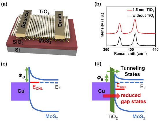
Figure 2.
(a) Fabrication schematic of the MoS2 FETs with a TiO2 interlayer; (b) Raman scattering spectra of the multilayer MoS2 without and with the TiO2 layer; (c,d) band diagrams of the MS structure and MIS structure.
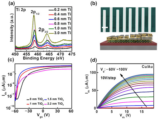
Figure 3.
(a) Ti 2p spectra of TiO2 with different thicknesses; (b) SEM image and schematic diagram of the back-gated Cu-TiO2-MoS2 FETs with various TiO2 thicknesses (0, 1, 1.5 and 2.2 nm) (scale bar = 5 µm); (c) transfer characteristics of the devices for various TiO2 thicknesses with L being 3 µm and Vds being 1 V; (d) output characteristics of the Cu-TiO2-MoS2 FETs.
The scanning electron microscopy (SEM) image and schematic diagram of the devices with different TiO2 interlayer thicknesses of 0, 1, 1.5 and 2.2 nm are exhibited in Figure 3b. Figure 3c shows the transfer characteristic curves of the device with various TiO2 thicknesses. The data are acquired at a source-drain voltage (Vds) of 1 V. Figure 3c shows that the source-drain current is largely dependent on the TiO2 interlayer thickness and the device with the 1.5 nm TiO2 interlayer shows the optimal characteristics. The increase in the drain current is mainly attributed to the reduced Schottky barrier and contact resistance. When the TiO2 interlayer thickness is 2.2 nm, a larger tunneling resistance is obtained; in addition, the source-drain current is reduced. The field-effect mobility µ can be estimated from the transfer curve by the following relationship:
where Cox is the gate capacitance, L = 3 µm is the length, W is the channel width and is the transconductance. As the gate voltage increases, the transconductance increases to a maximum value and then saturates. The extracted field-effect mobility values for the four TiO2 thicknesses (0, 1, 1.5 and 2.2 nm) are 27, 44, 58 and 11 cm2 V−1 s−1, respectively. The mobility of the device increases gradually after insertion of the TiO2 interface layer. When the thickness of the TiO2 interface layer is increased to 2.2 nm, the properties of the device begin to degrade. In particular, the mobility of the device with a 1.5 nm thick TiO2 interlayer increases by more than double compared to that before deposition of TiO2. Figure 3d shows the output characteristic curves of the device with 1.5 nm TiO2 thickness at different gate voltages (Vgs) ranging from −60 to 100 V. The device exhibits large current output and good cycling stability, further confirming that the insertion of the TiO2 interface layer improves the contact behavior. The results show that the TiO2 interlayer can improve the contact between the metal electrode and molybdenum disulfide. This may be because the intercalation of TiO2 avoids bonding between sulfur in molybdenum disulfide and the electrode metal; thus, this reduces the interface state and improves the contact compared to the evaporation of the metal electrode. To further elucidate the reasons for the improvement, Rc and ΦB are measured. The introduction of an interfacial layer at the contact reduces ΦB and increases the tunneling resistance. A thick interfacial layer results in a large tunneling resistance, but a small current flow through the device. Therefore, it is important to deposit an appropriate interfacial layer thickness to attain the best performance.
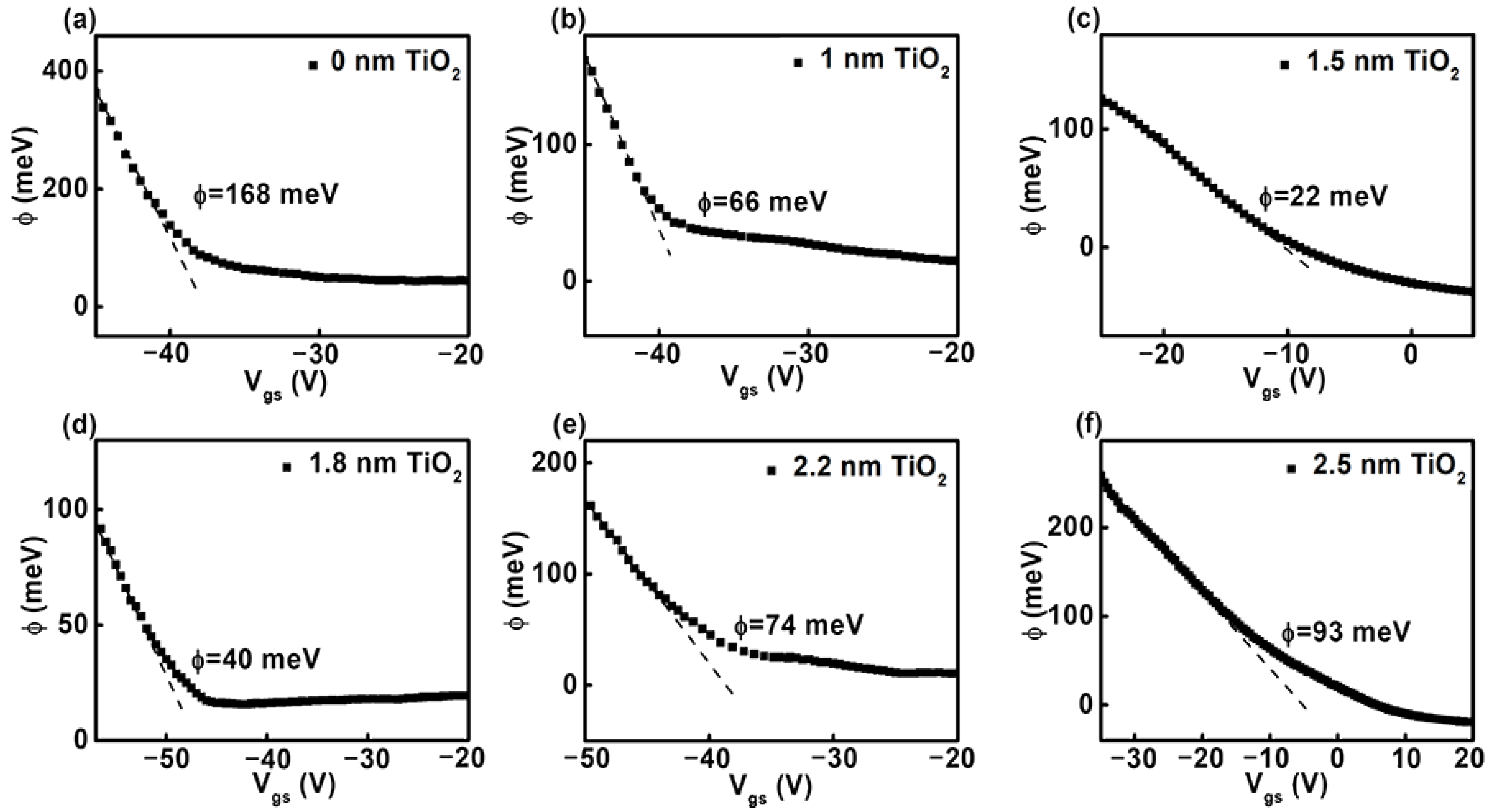
Contact resistance, an important performance indicator for transistors, is measured by the transmission line method (TLM). The contact resistances of the samples with various TiO2 thicknesses are shown in Figure 4. The gate voltage can adjust the carrier concentration of the molybdenum sulfide channel, thereby changing the contact resistance. Vg-t corresponds to the gate voltage minus threshold voltage. The device with the 1.5 nm TiO2 interlayer shows the minimum contact resistance of 4 kΩ·μm, which is smaller than the 8.2 kΩ·μm of that without the TiO2 interlayer. As the thickness of TiO2 is increased to 2.5 nm, Rc increases to 46 kΩ·μm and the large tunneling resistance results in poor performance. To further analyze the mechanism of Rc reduction, ΦB is measured to study the influence of different interlayer thicknesses. The Schottky barrier height is derived by the following formula [27,28]:
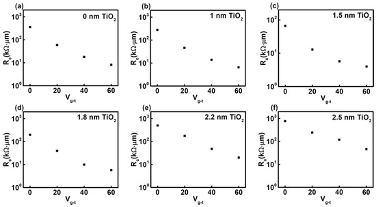
Figure 4.
(a–f) Contact resistances for various TiO2 thicknesses.
In this Equation (2), Ids is the current, A* is the Richardson’s constant, T is the temperature, q is the electronic charge, kB is the Boltzmann constant and Vds is the drain to source voltage. The effective barrier height here is different from that of the metal–semiconductor structures due to the insertion of the interfacial layer. Because insulators are not considered in expression (2) used to determine the barrier height, the effective barrier height given here represents the whole electronic behavior. When the gate bias is lower than the flat band voltage (Vfb), the device works in the thermionic emission state. The contribution of the tunneling current becomes significant when at a high gate bias (Vgs > Vfb) [29,30]. The slopes of these lines provide the effective Schottky barrier height, as shown in Figure 5a–f. ΦB at a flat band voltage for the device without the TiO2 layer is 168 meV (Figure 5a). Compared to ΦB without the TiO2 layer, ΦB of the device with the lowest Rc is 22 meV for a 1.5 nm TiO2 interfacial layer (Figure 5c). It is important that ΦB associated with Rc can be controlled by the thicknesses of the TiO2 layer. These results show that the metal–semiconductor contact interface is severely affected by Fermi level pinning; however, it is not greatly affected by the metal work function.
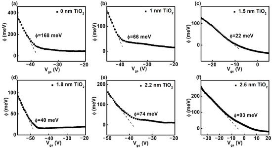
Figure 5.
(a–f) Effective Schottky barrier heights as a function of gate overdrive for various TiO2 thicknesses.
The MIS structures include two types of resistance: Schottky barrier resistance (RSB) and tunneling resistance (RT). Without an interlayer, a large ΦB causes a large RSB, which is the main part of the entire contact resistance. By inserting a TiO2 layer to reduce ΦB, RSB decreases accordingly. When the interfacial layer exceeds the optimal thickness, RT dominates the contact resistance; thus, this increases the overall contact resistance. By optimizing the thickness of the interfacial layer, a trade-off between RSB and RT can be obtained. The FETs with the 1.5 nm TiO2 layer have the minimum contact resistance, lowest Schottky barrier height and optimal properties consistent with Figure 3c. The TiO2 interface layer has two functions: first, it obtains a reduced Schottky barrier and contact resistance in the source-drain contact area; and second, it acts as a dielectric shield and increases charge density at the TiO2–MoS2 interface. At the same time, the moisture and oxygen in the air are isolated; moreover, the stability of the device is improved. Using TiO2 as an interfacial layer results in the lowest ΦB because of the small conduction band offset between MoS2 and TiO2, which is more conducive to carrier injection.
4. Conclusions
The N-type MoS2 field-effect device with good contact is fabricated by using TiO2 as the interlayer between MoS2 and the metal electrode. By evaporating a low melting point metal and then, performing re-oxidation, damage is avoided in the materials; in addition, the stability of the equipment is ensured. The effect of the interlayer thickness on the device characteristics is investigated systematically. The thickness of the interfacial layer plays a crucial role in the device properties. The device with a 1.5 nm thick TiO2 as the interfacial layer shows a small ΦB of 22 meV and a low Rc of 4 kΩ·µm. The results provide important clues to contact engineering and how to improve 2D semiconductor devices. The MIS structure is also effective in solving the contact problems and presents a potential solution for contacts in devices based on 2D materials.
Author Contributions
Conceptualization, J.C.; data curation, C.L.; formal analysis, J.H. and H.Y.; investigation, D.Z.; methodology, C.P.; project administration, J.C.; software, X.H.; writing—original draft, J.C.; writing—review and editing, P.K.C. All authors have read and agreed to the published version of the manuscript.
Funding
This work was financially supported by the Natural Science Foundation of Henan Province (222300420255 and 222300420506); Key Scientific and Technological Project of Technology Department of Henan Province of China (212102210448 and 222102230105); Science Fund of Educational Department of Henan Province of China (21A140020); City University of Hong Kong Donation Research Grant (DON-RMG No. 9229021); as well as Shenzhen-Hong Kong Innovative Collaborative Research and Development Program (SGLH20181109110802117 and CityU 9240014).
Institutional Review Board Statement
Not applicable.
Informed Consent Statement
Not applicable.
Data Availability Statement
Not applicable.
Conflicts of Interest
The authors declare no conflict of interest.
References
- Zhang, X.; Li, Y.; Mu, W.; Bai, W.; Sun, X.; Zhao, M.; Zhang, Z.; Shan, F.; Yang, Z. Advanced tape-exfoliated method for preparing large-area 2D monolayers: A review. 2D Mater. 2021, 8, 032002. [Google Scholar] [CrossRef]
- Hwangbo, S.; Hu, L.; Hoang, A.T.; Choi, J.Y.; Ahn, J.-H. Wafer-scale monolithic integration of full-colour micro-LED display using MoS2 transistor. Nat. Nanotechnol. 2022, 17, 500–506. [Google Scholar] [CrossRef] [PubMed]
- Zhou, Y.; Wang, Y.; Zhuge, F.; Guo, J.; Ma, S.; Wang, J.; Tang, Z.; Li, Y.; Miao, X.; He, Y.; et al. A Reconfigurable Two-WSe2-Transistor Synaptic Cell for Reinforcement Learning. Adv. Mater. 2022, 2107754. [Google Scholar] [CrossRef]
- Tang, Y.; Huang, C.-H.; Nomura, K. Vacuum-Free Liquid-Metal-Printed 2D Indium-Tin Oxide Thin-Film Transistor for Oxide Inverters. ACS Nano 2022, 16, 3280–3289. [Google Scholar] [CrossRef]
- Lee, D.; Choi, Y.; Kim, J.; Kim, J. Recessed-Channel WSe2 Field-Effect Transistor via Self-Terminated Doping and Layer-by-Layer Etching. ACS Nano 2022, 16, 8484–8492. [Google Scholar] [CrossRef] [PubMed]
- Wu, H.; Cui, Y.; Xu, J.; Yan, Z.; Xie, Z.; Hu, Y.; Zhu, S. Multifunctional Half-Floating-Gate Field-Effect Transistor Based on MoS2-BN-Graphene van der Waals Heterostructures. Nano Lett. 2022, 22, 2328–2333. [Google Scholar] [CrossRef]
- Cheng, J.; Wang, C.; Zou, X.; Liao, L. Recent Advances in Optoelectronic Devices Based on 2D Materials and Their Heterostructures. Adv. Opt. Mater. 2018, 7, 1800441. [Google Scholar] [CrossRef]
- Geim, A.K.; Novoselov, K.S. The rise of graphene. Nat. Mater. 2007, 6, 183–191. [Google Scholar] [CrossRef]
- Novoselov, K.S.; Geim, A.K.; Morozov, S.V.; Jiang, D.; Zhang, Y.; Dubonos, S.V.; Grigorieva, I.V.; Firsov, A.A. Electric Field Effect in Atomically Thin Carbon Films. Science 2004, 306, 666–669. [Google Scholar] [CrossRef]
- Mak, K.F.; Lee, C.; Hone, J.; Shan, J.; Heinz, T.F. Atomically Thin MoS2: A New Direct-Gap Semiconductor. Phys. Rev. Lett. 2010, 105, 136805. [Google Scholar] [CrossRef] [Green Version]
- Kuc, A.; Zibouche, N.; Heine, T. Influence of quantum confinement on the electronic structure of the transition metal sulfide TS2. Phys. Rev. B 2011, 83, 245213. [Google Scholar] [CrossRef]
- Yu, Z.; Pan, Y.; Shen, Y.; Wang, Z.; Ong, Z.-Y.; Xu, T.; Xin, R.; Pan, L.; Wang, B.; Sun, L.; et al. Towards intrinsic charge transport in monolayer molybdenum disulfide by defect and interface engineering. Nat. Commun. 2014, 5, 5290. [Google Scholar] [CrossRef] [PubMed]
- Yoon, Y.; Ganapathi, K.; Salahuddin, S. How Good Can Monolayer MoS2 Transistors Be? Nano Lett. 2011, 11, 3768–3773. [Google Scholar] [CrossRef]
- Popov, I.; Seifert, G.; Tomanek, D. Designing Electrical Contacts to MoS2 Monolayers: A Computational Study. Phys. Rev. Lett. 2012, 108, 156802. [Google Scholar] [CrossRef] [PubMed]
- Du, H.; Kim, T.; Shin, S.; Kim, D.; Kim, H.; Sung, J.H.; Lee, M.J.; Seo, D.H.; Lee, S.K.; Jo, M.-H.; et al. Schottky barrier contrasts in single and bi-layer graphene contacts for MoS2 field-effect transistors. Appl. Phys. Lett. 2015, 107, 233106. [Google Scholar] [CrossRef]
- Du, Y.; Liu, H.; Neal, A.T.; Si, M.; Ye, P.D. Molecular Doping of Multilayer MoS2 Field-Effect Transistors: Reduction in Sheet and Contact Resistances. IEEE Electron. Device Lett. 2013, 34, 1328–1330. [Google Scholar] [CrossRef]
- Das, S.; Chen, H.-Y.; Penumatcha, A.V.; Appenzeller, J. High Performance Multilayer MoS2 Transistors with Scandium Contacts. Nano Lett. 2013, 13, 100–105. [Google Scholar] [CrossRef]
- Lee, S.; Tang, A.; Aloni, S.; Wong, H.-S.P. Statistical Study on the Schottky Barrier Reduction of Tunneling Contacts to CVD Synthesized MoS2. Nano Lett. 2016, 16, 276–281. [Google Scholar] [CrossRef]
- Wang, J.; Yao, Q.; Huang, C.-W.; Zou, X.; Liao, L.; Chen, S.; Fan, Z.; Zhang, K.; Wu, W.; Xiao, X.; et al. High Mobility MoS2 Transistor with Low Schottky Barrier Contact by Using Atomic Thick h-BN as a Tunneling Layer. Adv. Mater. 2016, 28, 8302–8308. [Google Scholar] [CrossRef]
- Kim, Y.; Park, W.; Yang, J.H.; Cho, C.; Lee, S.K.; Lee, B.H. Reduction of low-frequency noise in multilayer MoS2 FETs using a Fermi-level depinning layer. Phys. Status Solidi RRL 2016, 10, 634–638. [Google Scholar] [CrossRef]
- Simsek, E.B. Solvothermal synthesized boron doped TiO2 catalysts: Photocatalytic degradation of endocrine disrupting compounds and pharmaceuticals under visible light irradiation. Appl. Catal. B Environ. 2017, 200, 309–322. [Google Scholar] [CrossRef]
- Shi, Z.; Yang, P.; Tao, F.; Zhou, R. New insight into the structure of CeO2-TiO2 mixed oxides and their excellent catalytic performances for 1,2-dichloroethane oxidation. Chem. Eng. J. 2016, 295, 99–108. [Google Scholar] [CrossRef]
- Heine, V. Theory of Surface States. Phys. Rev. 1965, 138, A1689–A1696. [Google Scholar] [CrossRef]
- Tersoff, J. Schottky Barrier Heights and the Continuum of Gap States. Phys. Rev. Lett. 1984, 52, 465. [Google Scholar] [CrossRef]
- Hu, J.; Saraswat, K.C.; Wong Philip, H.-S. Metal/III-V effective barrier height tuning using atomic layer deposition of high-κ/high-κ bilayer interfaces. Appl. Phys. Lett. 2011, 99, 092107. [Google Scholar] [CrossRef]
- Hu, J.; Saraswat, K.C.; Wong Philip, H.-S. Metal/III-V Schottky barrier height tuning for the design of nonalloyed III-V field-effect transistor source/drain contacts. J. Appl. Phys. 2010, 107, 063712. [Google Scholar] [CrossRef]
- Wang, W.; Liu, Y.; Tang, L.; Jin, Y.; Zhao, T.; Xiu, F. Controllable Schottky Barriers between MoS2 and Permalloy. Sci. Rep. 2014, 4, 6928. [Google Scholar] [CrossRef]
- Farmanbar, M.; Brocks, G. Controlling the Schottky barrier at MoS2/metal contacts by inserting a BN monolayer. Phys. Rev. B 2015, 91, 161304. [Google Scholar] [CrossRef]
- Anugrah, Y.; Robbins, M.C.; Crowell, P.A.; Koester, S.J. Determination of the Schottky barrier height of ferromagnetic contacts to few-layer phosphorene. Appl. Phys. Lett. 2015, 106, 103108. [Google Scholar] [CrossRef]
- Allain, A.; Kang, J.; Banerjee, K.; Kis, A. Electrical contacts to two-dimensional semiconductors. Nat. Mater. 2015, 14, 1195–1205. [Google Scholar] [CrossRef]


Publisher’s Note: MDPI stays neutral with regard to jurisdictional claims in published maps and institutional affiliations. |
© 2022 by the authors. Licensee MDPI, Basel, Switzerland. This article is an open access article distributed under the terms and conditions of the Creative Commons Attribution (CC BY) license (https://creativecommons.org/licenses/by/4.0/).