


Abstract
High-power bidirectional dc–dc converters are being widely employed in renewable energy interfacing, energy storage, electric vehicle charging, military, aerospace, and marine applications. Among various bidirectional topologies documented in the literature for dc–dc power conversion, the split-pi converter invites special attention with regard to applications involving multi-phase systems requiring high-power density. This paper endeavors to present the small-signal modeling of the split-pi converter in its various operating modes. Subsequently, the dynamic characteristics of the converter are studied, and appropriate control design is presented for stable operation of the converter. Frequency response plots are illustrated, and a hardware prototype model of the converter is designed and implemented.
1. Introduction
Multiple applications involving aerospace, military, marine, and transport electrification and renewable energy integration necessitate high-efficiency dc power converters with stable bidirectional operation and high-power density. Quite a lot of topologies have been proposed by researchers for bidirectional dc–dc conversion in the past few years to suit various applications [1,2,3,4,5,6,7,8,9,10,11,12]. These topologies are either isolated or nonisolated allowing a bidirectional power flow. Further, these topologies operating in boost, buck, or buck–boost mode depending on the placement of passive elements. Amid various topologies proposed in the literature, the split-pi converter (SPC) is the one that draws exclusive interest owing to its remarkable features viz., high conversion efficiency, capability to operate in various switching modes, and bidirectional power flow. Additionally, its nonisolated structure and high-frequency operation along with the lower ratings of passive elements make it an apt choice for applications demanding high-power density [13,14]. Unlike the classic buck–boost topology, this topology overcomes the voltage gain limitations of the converter and is prone to minimal voltage and current fluctuations. Parallel connection is also possible with this converter topology and hence can be used in multiphase systems. A reduction in switching noise is achieved as the LC filters at either port of the converter favor small reactive components. Moreover, the control circuit of SPC topology involves simple duty cycle control of the PWM signal and is hence less laborious [15,16,17].
The aforementioned advantages of the SPC makes it ideally suited for electric vehicles and energy storage applications, among others. With the direction of current flow changing from instant to instant in these applications, a dynamic analysis of the converter is essential. In addition, an appropriate control design is essential in enhancing the overall performance of the system. Hence, this paper intends to present in detail the small-signal modeling of the SPC along with the control design for all the switching modes. Though the SPC topology was introduced in 2014 [18], very little literature is available related to the modeling and control design of the converter. A state–space averaging model of the SPC followed by a type-II compensator design is described in [19]. However, the state–space model is derived only for boost mode of operation of the converter, and the prototype design and experimental results are not presented. In [20], the authors have proposed a multilevel and symmetrical structure for the SPC and compared it with the interleaved topology. Few details pertaining to the control design with controlled current or voltage feedback and dc link voltage have been presented. Elaborate state–space models of the SPC with respect to energy storage interface of stiff and nonstiff dc microgrids have been discussed in [21]. A unique control strategy for controlling the flywheel system using the SPC in rural applications has been described in [22]. Thus, a generalized modeling and control design for different operation modes of the conventional SPC topology is not available in the literature according to the authors.
This paper attempts to explain in detail the small-signal modeling of the SPC topology followed by the control design for various operating modes. In addition, a stability analysis was carried out through frequency response plots, and a stable control design is presented for both the buck and boost modes of operation of the converter. An experimental prototype of the SPC was developed with the designed closed loop control, and the results are demonstrated to validate the design.
2. Small-Signal Modeling: Split-Pi Converter
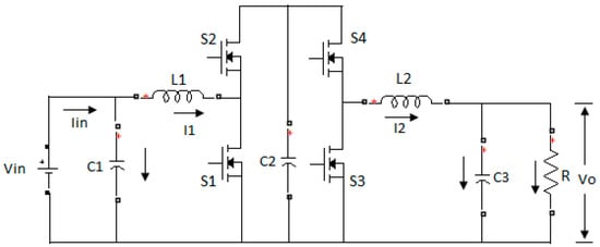
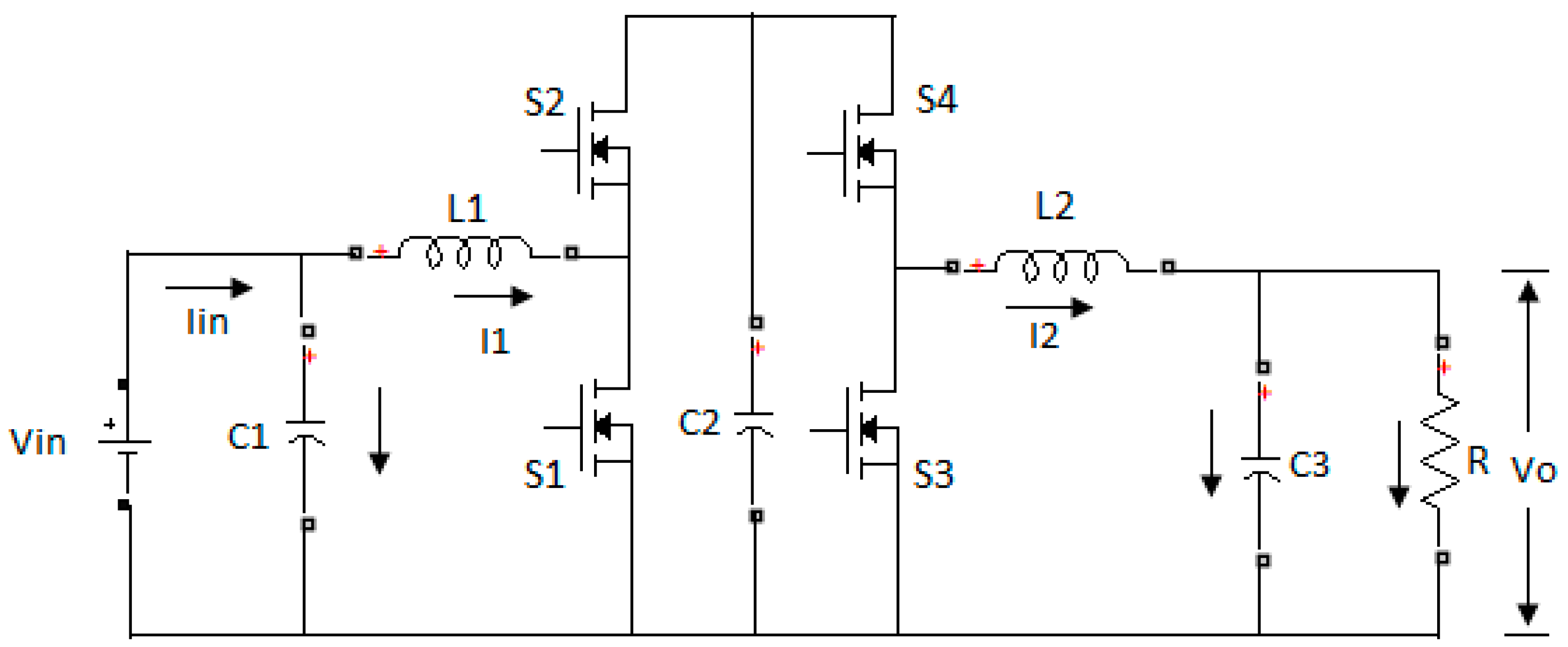
The schematic of SPC topology is illustrated in Figure 1. The circuit comprises a boost topology followed by a buck topology. Thus, this converter is capable of operating in three different modes, namely, the boost, buck, and pass-through modes. Of the four switches available, only two conducts at any point of time in all the three switching modes provide the required output. While the buck and boost modes of operation are already familiar, the pass-through mode simply passes the input to the output. The mathematical analysis of the different modes of operation is presented below followed by the small-signal modeling.
Figure 1.
Circuit topology of SPC.
2.1. Boost Mode
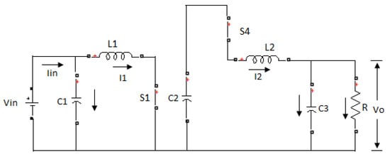
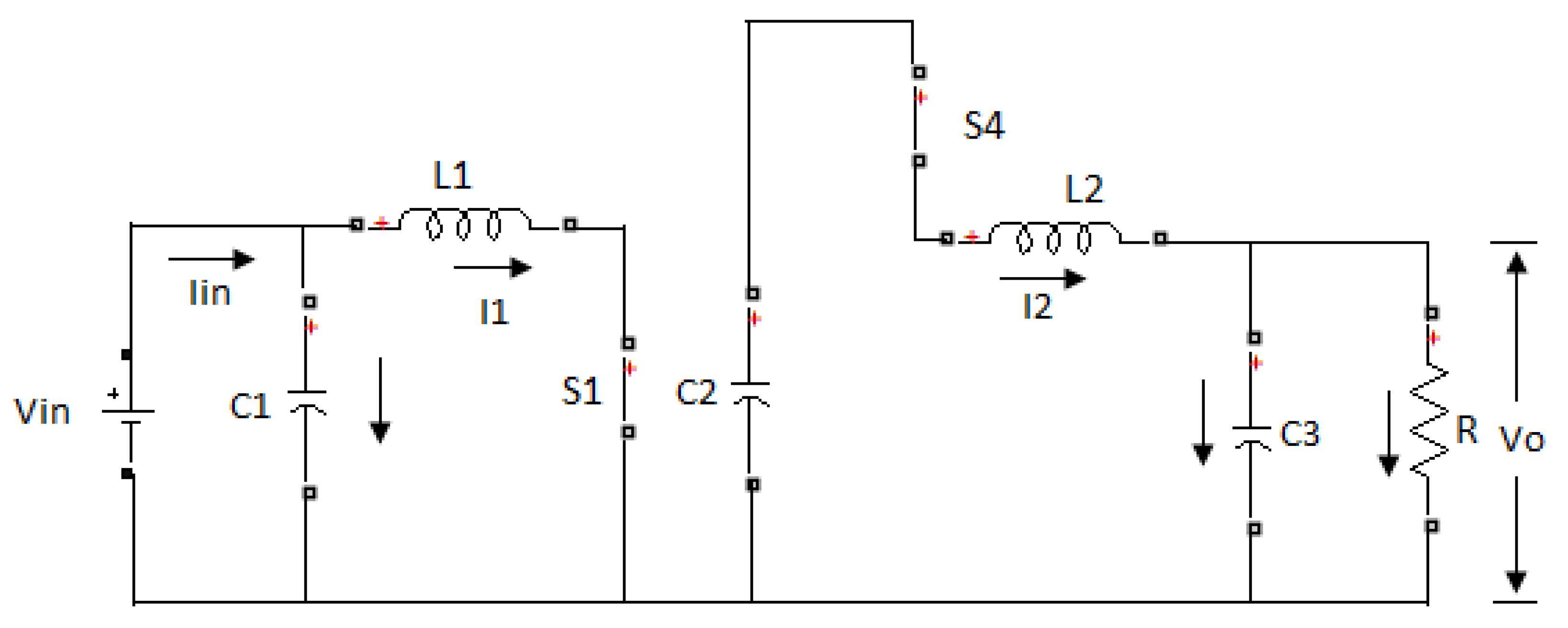
In the boost mode of operation, switch S4 is always ON, and S3 is always OFF. S1 and S2 are switched alternatively so that boost voltage is available at the output. The two modes of operation are described below
Mode 1:
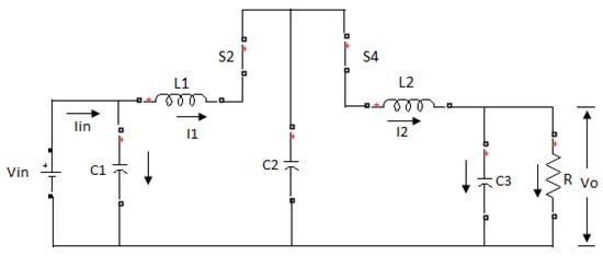
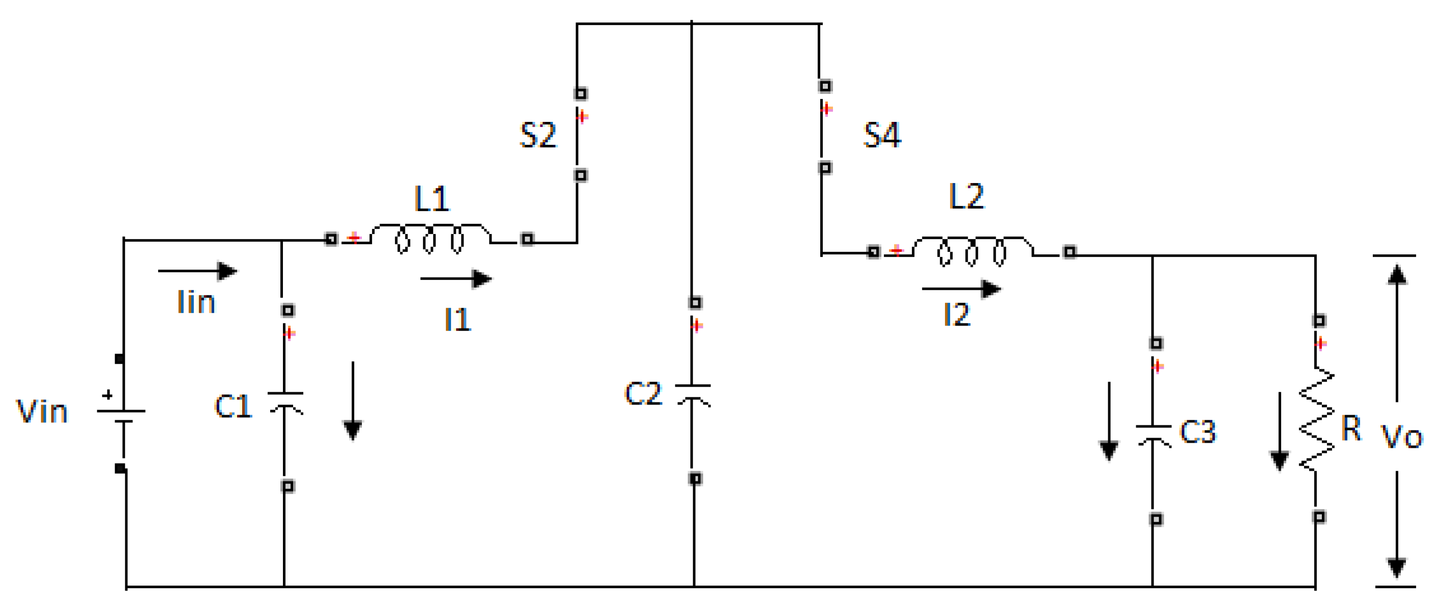
The circuit schematic during mode 1 is depicted in Figure 2. Switches S1 and S3 are OFF, and S2 and S4 are turned ON. The differential equations governing the circuit operation are listed as follows:
Figure 2.
Circuit schematic of SPC during mode 1 under boost operation.
Applying KVL and KCL to the circuit in Figure 2, we have the following set of equations for the voltage across the inductors and current through the capacitors:
The state Equations (1)–(5) can be expressed as
The output equation for this mode is
Equation (8) can be expressed as
Mode 2:
The circuit schematic during mode 2 is depicted in Figure 3. Switches S2 and S3 are OFF, and S1 and S4 are turned ON. The differential equations governing the circuit operation are listed as follows:
Figure 3.
Circuit schematic of SPC during mode 2 under boost operation.
Applying KVL and KCL to the circuit above, we have the following set of equations for voltage across the inductors and current through the capacitors:
Combining Equations (10)–(14) in matrix form,
The output equation is the same as Equation (8).
Applying state–space averaging, the state coefficient matrix A can be expressed as
where d is the duty cycle of switch S1.
The averaged source coefficient matrix is given by
Similarly,
Thus, the state–space averaged equations in matrix form are given by
The above matrix can be expanded to give the averaged state–space equations:
The small-signal model is used for deriving the compensators that can realize the control objective of keeping the output voltage constant while drawing constant power from the sources. In order to derive small-signal models, the averaged equations must contain small signal variables. This is done by replacing each variable with both a DC and an AC value. Assuming a stiff voltage across the capacitor C2 and applying small-signal perturbations to other electrical quantities, the Equations (20)–(22) and (24) are represented as
The dc or steady-state solutions of the above set of equations are:
The dynamic or ac solutions are:
Representing Equations (33)–(36) in matrix form,
The above matrix equation is of the form
Laplace transform of the above equation yields
where is the identity matrix. In Equation (38), is a function of x and u and termed as the control law. The control law is usually nonlinear, and its linearized model can be written as
where and are the coefficient matrices for voltage mode PWM control, and H(s) denotes the transfer function of the error amplifier and its compensation network, and is the peak amplitude of the sawtooth signal [23].
Substituting Equation (39) into Equation (38), we have
The source-to-state transfer functions for the SPC can be obtained by substituting for and into Equation (40). Thus, the state variable matrix is
From Equation (41), the small-signal transfer functions can be obtained,
The small-signal control transfer function can be obtained by substituting in Equation (38).
Therefore,
The open-loop transfer function of inductor current L1 is thus given by
and the open-loop transfer function of input capacitor voltage C1 is given by
2.2. Buck Mode
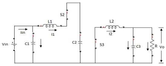
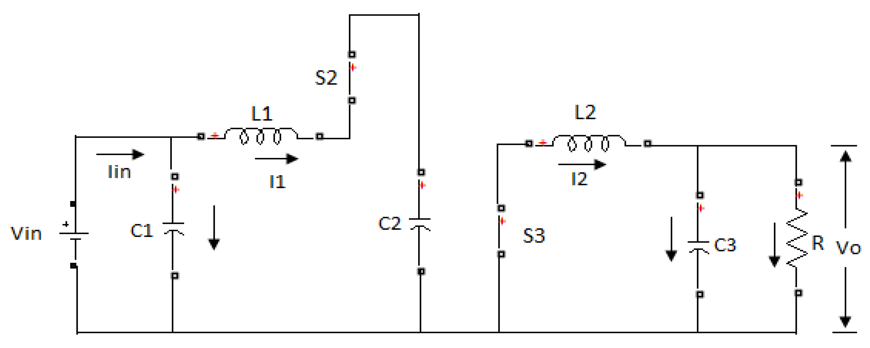
In the buck mode of operation, switch S2 is always ON, and S1 is always OFF. S3 and S4 are switched alternatively so that the buck voltage is available at the output. The two operation modes are described below [24].
Mode 1:
The circuit schematic during mode 1 is depicted in Figure 4. Switches S1 and S4 are OFF, and S2 and S3 are turned ON. The differential equations governing the circuit operation are listed as follows:
Figure 4.
Circuit schematic of SPC during mode 1 under buck operation.
The state Equations (45)–(49) can be expressed as
The output equation for this mode is
Equation (51) can be written in matrix form as
Mode 2:
Figure 5 represents the circuit schematic during mode 2. Switches S1 and S3 are OFF, and S2 and S4 are turned ON. The differential equations describing the circuit operation are given below [25]:
Figure 5.
Circuit schematic of SPC during mode 2 under buck operation.
Applying KVL and KCL to the circuit above, we have the following set of equations for the voltage across the inductors and current through the capacitors:
The state Equations (52)–(56) can be written in matrix form as
The output equation for this mode is
Equation (58) can be expressed as
Applying state–space averaging, the state coefficient matrix A can be written as
where d is the duty cycle of the converter.
The averaged source coefficient matrix is given by
Similarly,
Thus, the state–space averaged equations in matrix form are given by
The above matrix can be expanded to give the averaged state–space equations:
Assuming a stiff voltage across the capacitor C2 and applying small-signal perturbations to other electrical quantities, the Equations (63)–(65) and (67) are represented as
The dc or steady-state solutions of the above set of equations are
The dynamic or ac solutions are:
Representing Equations (76)–(79) in matrix form,
The above matrix equation is of the form
Referring to Equation (40), the state variable matrix is
From Equation (79), the small-signal transfer functions can be obtained,
The small-signal control transfer function can be obtained by substituting in Equation (38).
Therefore,
The inductor current L2 and the capacitor voltage C3 are thus given by
2.3. Pass-Through Mode
In pass-through mode, switches S1 and S3 are permanently switched OFF, and switches S2 and S4 are permanently switched ON. The input voltage is directly passed on to the output. Hence no controller is required for this mode.
3. Control Design of Split-Pi Converter
Following the mathematical analysis and small-signal modeling of the SPC, the open loop transfer functions of the input current and output voltage are derived in the previous section. Now, with the available transfer functions, a sample case study of the control design is carried out using MATLAB SISOTOOL for both the boost and buck modes of operation [26].
The converter ratings for the sample case study are furnished in Table 1.
Table 1.
Ratings of the SPC.
3.1. Boost Mode of Operation
With the converter ratings given in Table 1, the controller for boost mode operation can be designed. Substituting the converter ratings in Equation (44), we have
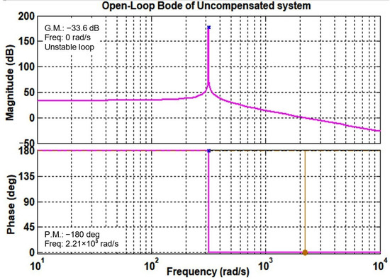
The system represented by the transfer function in (85) is marginally stable with open-loop poles on the imaginary axis. The root locus and Bode plots for are presented in Figure 6 and Figure 7, respectively.
Figure 6.
Root locus plot of Gvd represented in Equation (86).
Figure 7.
Open-loop Bode plot of Gvd represented in Equation (86).
It is understood from the above plots that the open-loop system represented by the transfer function in Equation (86) is unstable. Therefore, a suitable compensator has to be inserted to make it stable.
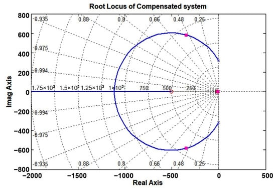
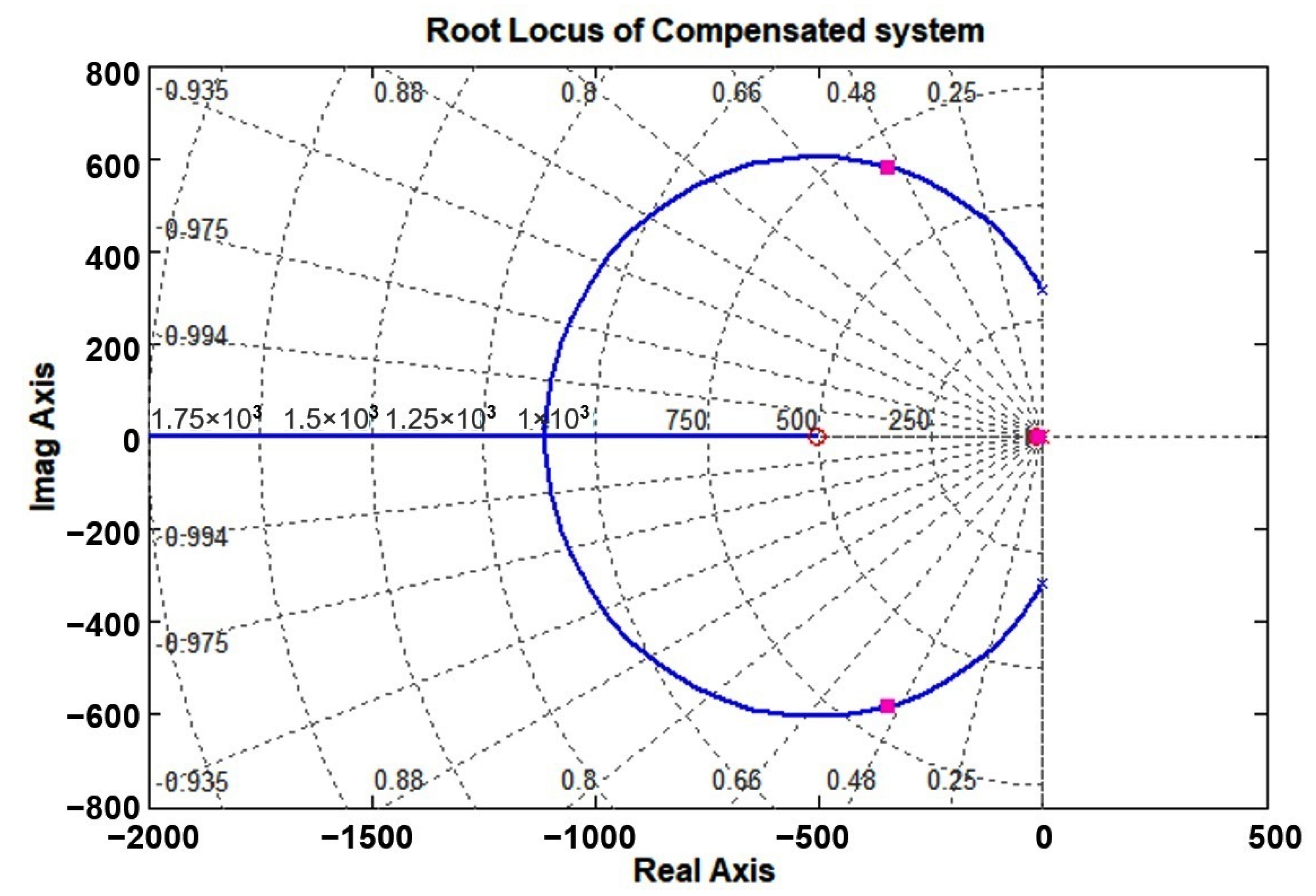
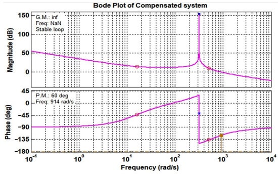
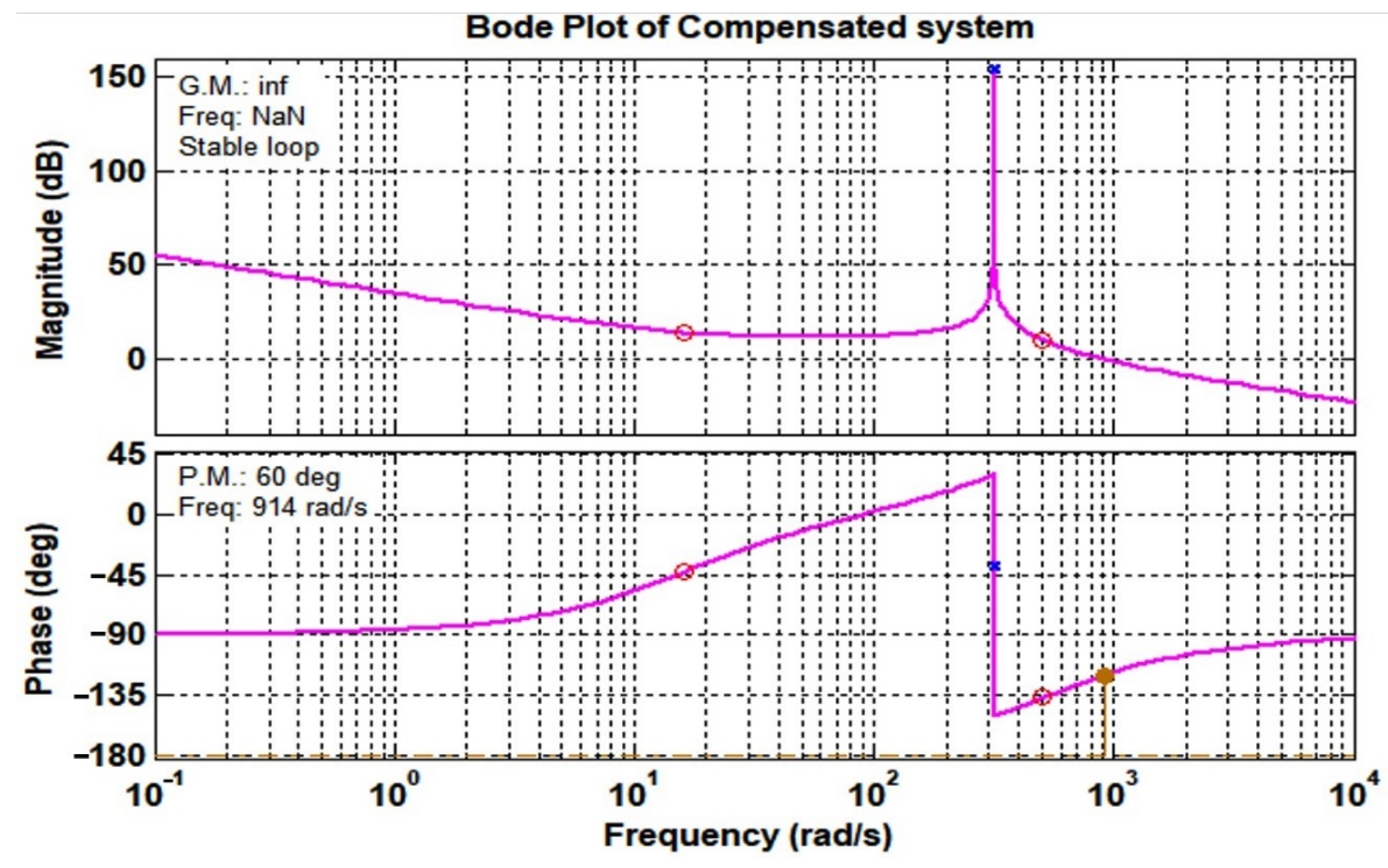
The compensator design is performed through MATLAB SISOTOOL. The PID tuning method was adopted for the design. The compensator transfer function after suitable tuning is given by
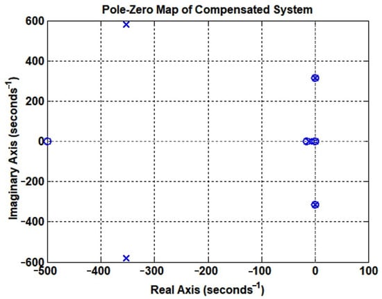
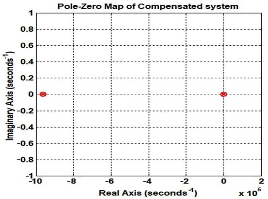
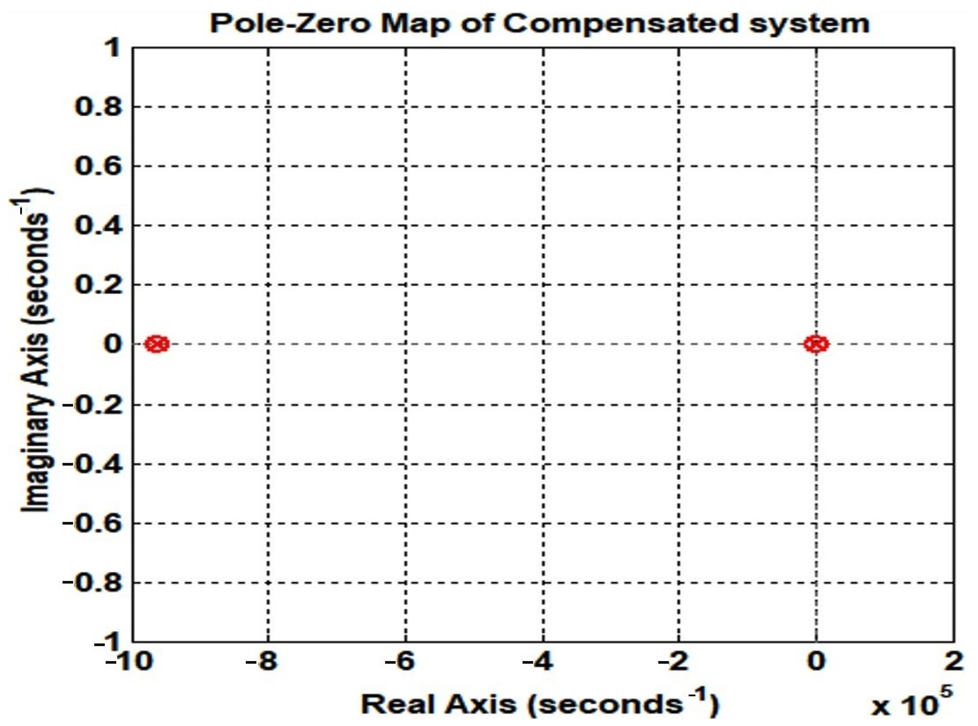
with a pole at origin (p = 0) and two zeros on the negative real axis (z = −499.848, −15.8774) The closed-loop transfer function of the system with the compensator is given by
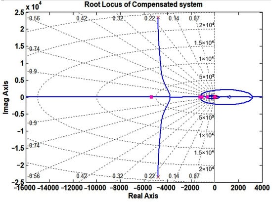
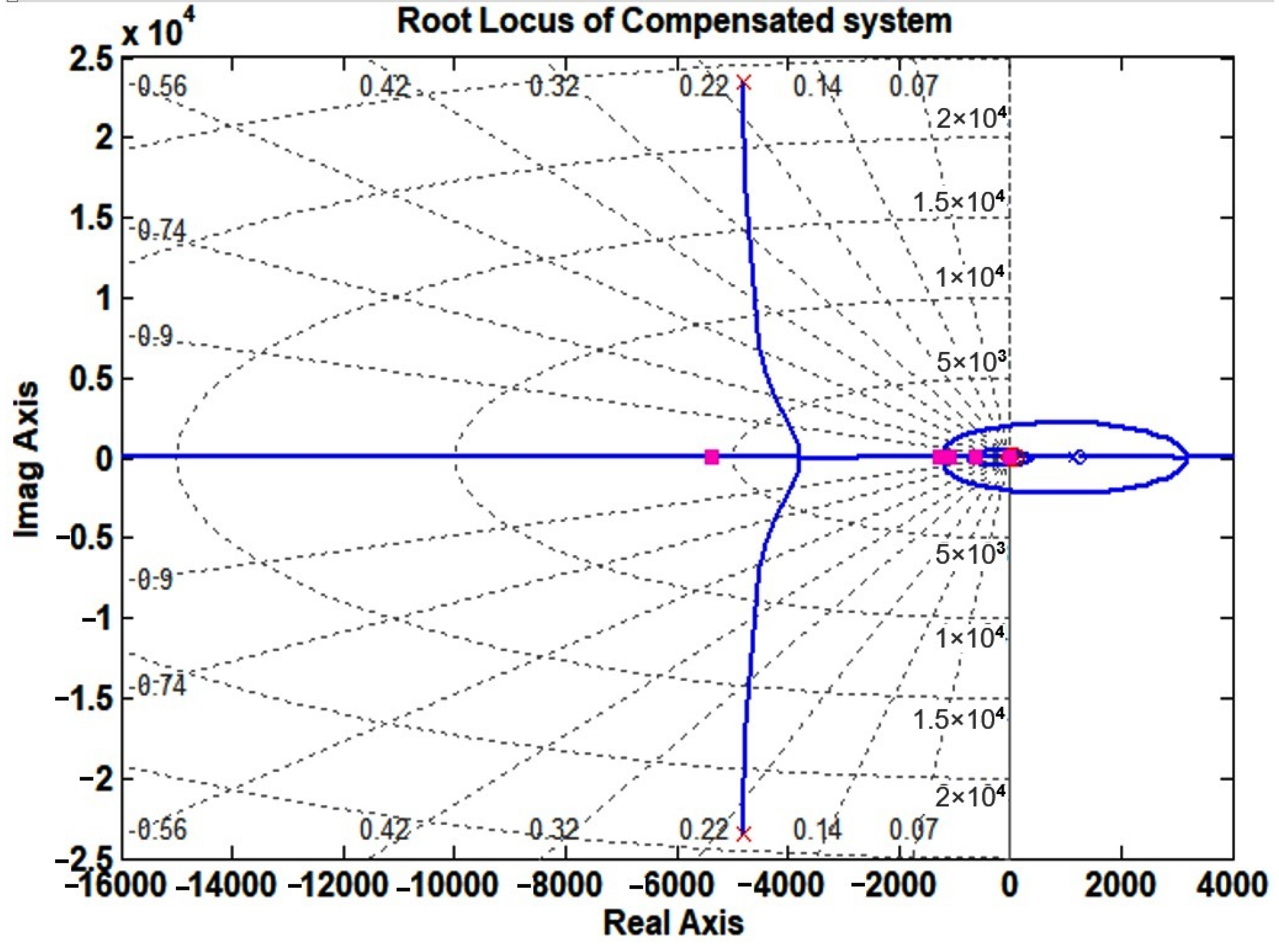
The pole-zero map, root locus, and Bode plots of the compensated system are depicted in Figure 8, Figure 9 and Figure 10, respectively.
Figure 8.
Pole-zero map of Gvd with the designed compensator.
Figure 9.
Root locus plot of Gvd with the designed compensator.
Figure 10.
Bode plot of Gvd with the designed compensator.
The compensated system is observed to have an infinite gain margin at a phase crossover frequency of 916 rad/s and a phase margin of 120°. The system is thus stable.
3.2. Buck Mode of Operation
The controller for the buck mode of operation can be designed in this section. Substituting the converter ratings given in Table 1 into Equation (84), we have
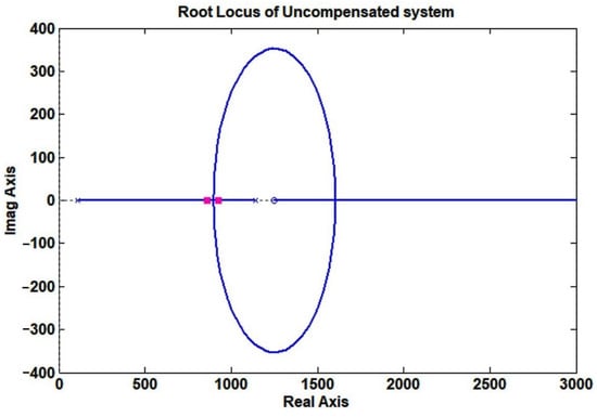
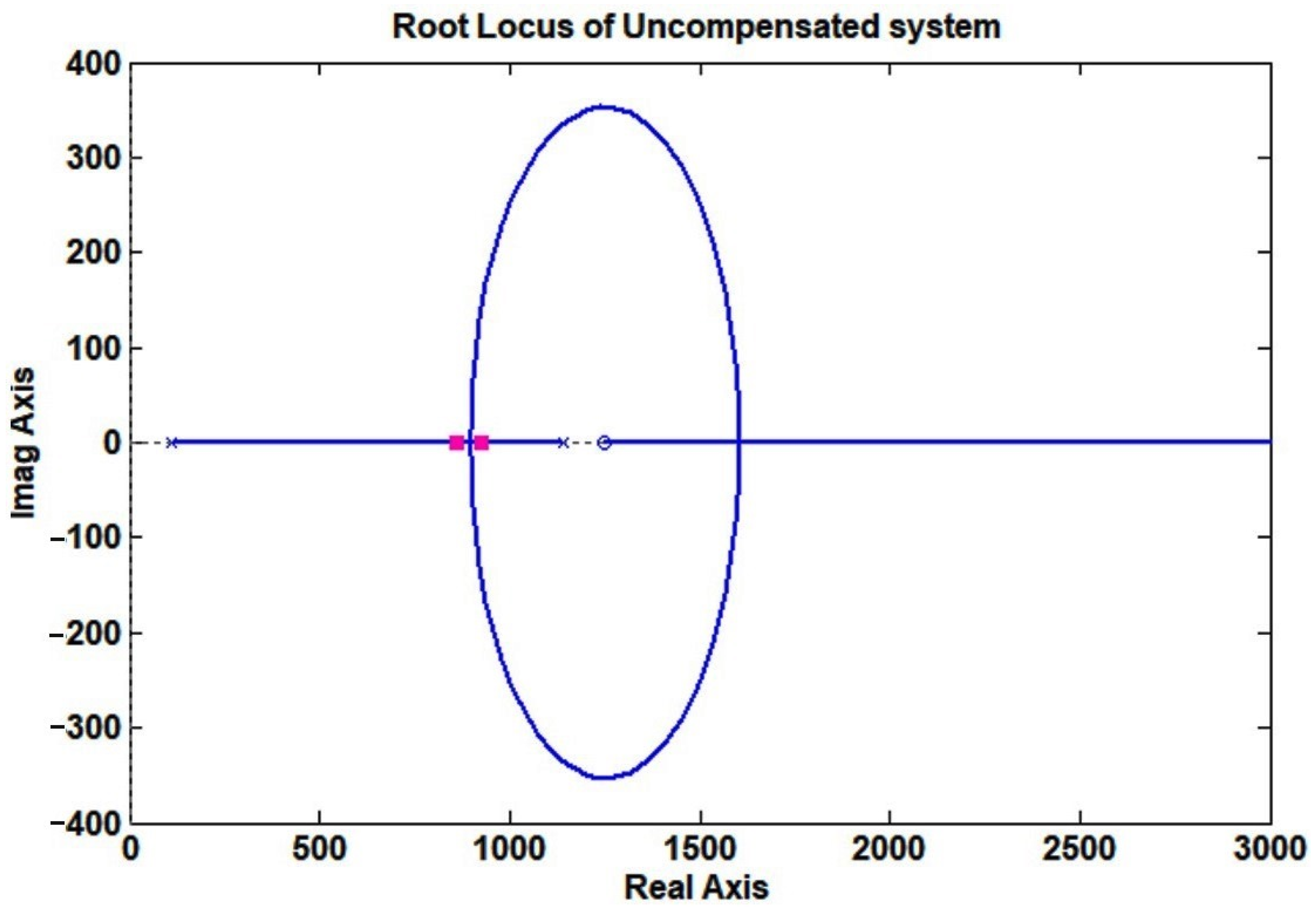
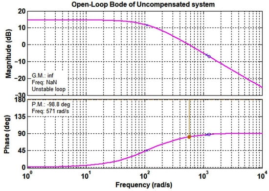
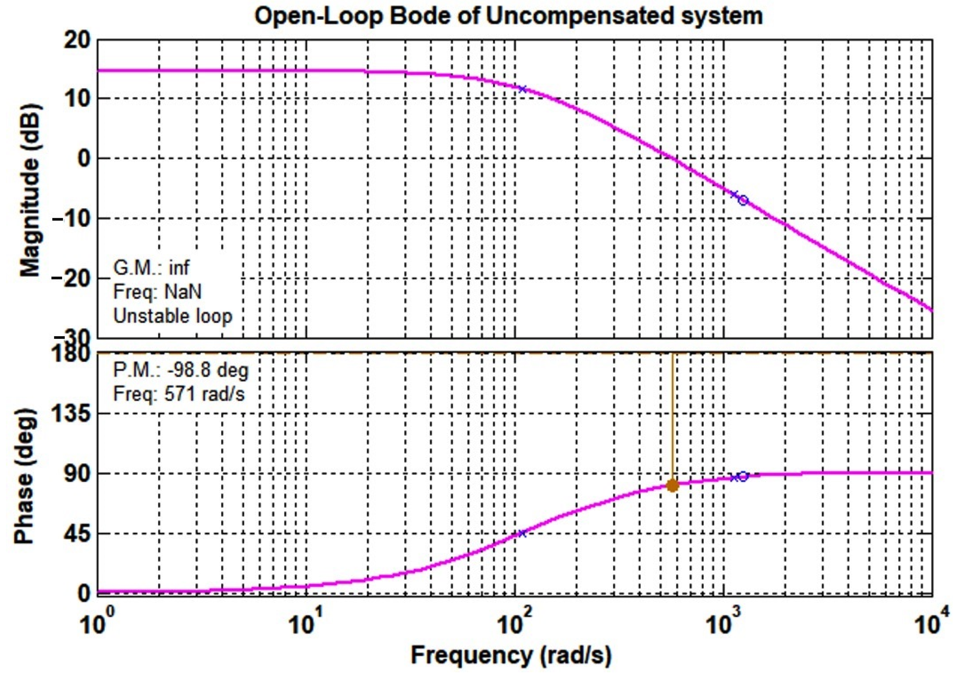
The system represented by the transfer function in Equation (90) is unstable with two poles (p = 1140, 109.6) and a zero (z = 1250) on the positive real axis. The root locus and Bode plots for the system are shown in Figure 11 and Figure 12, respectively.
Figure 11.
Root locus plot of Gid represented in Equation (92).
Figure 12.
Bode plot of Gid represented in Equation (92).
It is understood from the above plots that the closed-loop system represented by the transfer function in Equation (92) is unstable. Therefore, a suitable compensator has to be inserted to make it stable.
The compensator design is performed through MATLAB SISOTOOL. The LQG synthesis method was adopted for the design. The compensator transfer function after suitable tuning is given by
with three poles (p = 0,) and two zeros (z = 99.933, 0.0667).
The closed-loop transfer function of the system with the compensator is given by
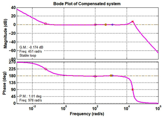
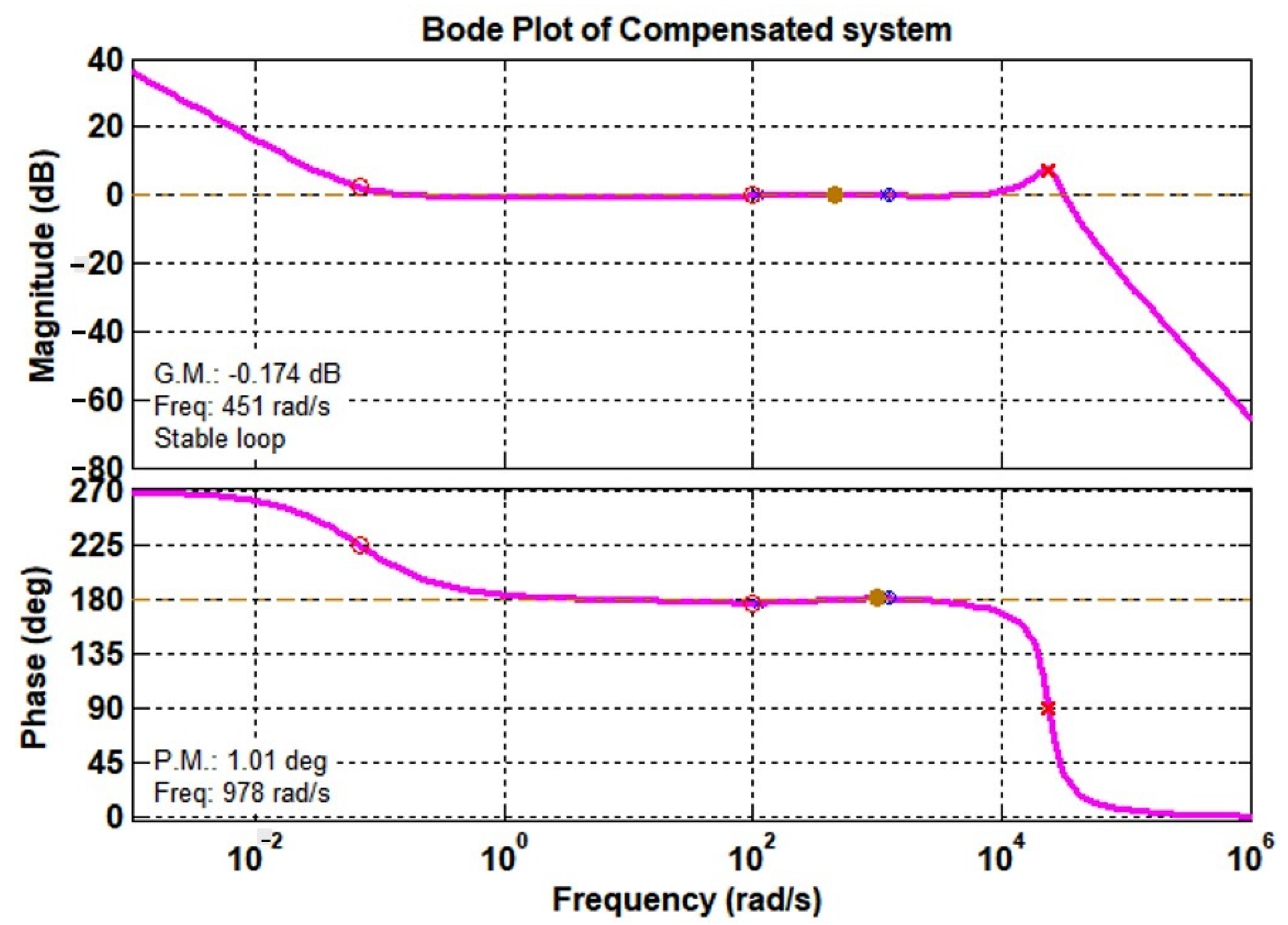
The pole-zero map, root locus, and Bode plots of the compensated system are depicted in Figure 13, Figure 14 and Figure 15.
Figure 13.
Pole-zero map of Gid with the designed compensator.
Figure 14.
Root locus plot of Gid with the designed compensator.
Figure 15.
Bode plot of Gid with the designed compensator.
4. Experimental Prototype of Split-Pi Converter
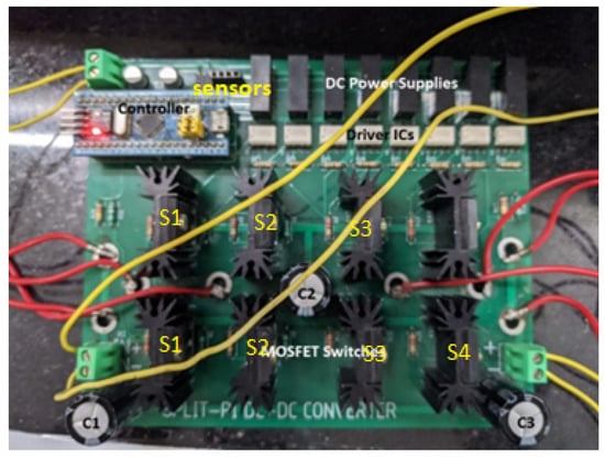
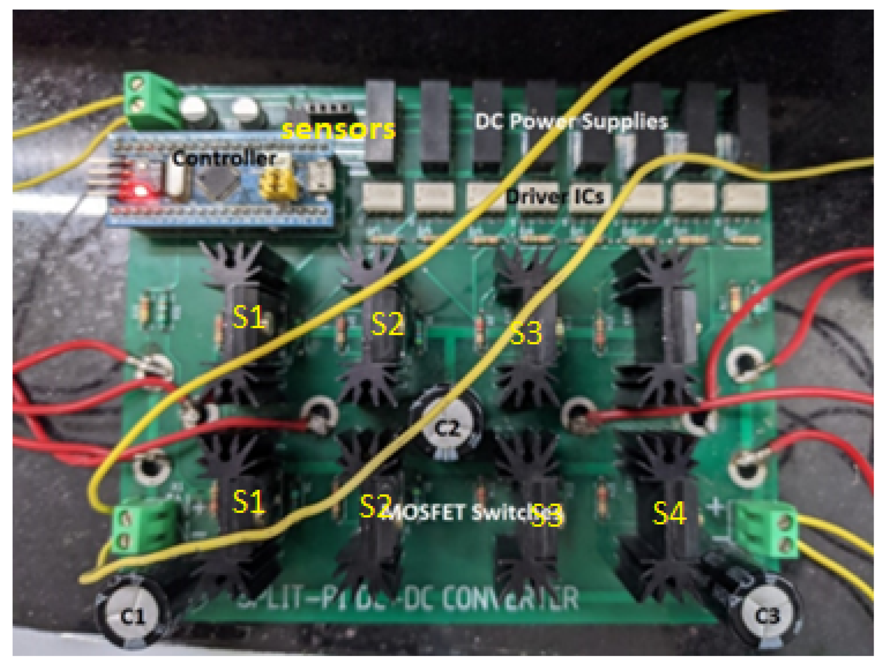
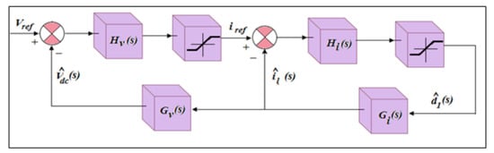
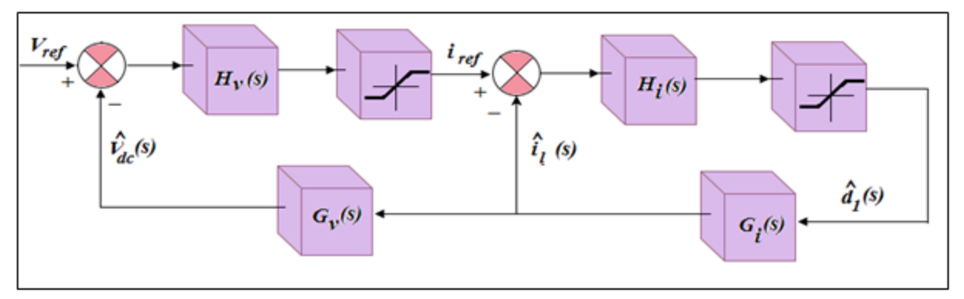
An experimental hardware of 500 W SPC was constructed as shown in Figure 16 to verify its operation. The hardware ratings and component specifications are listed in Table 2 The STM32 controller was used to generate switching pulses to the converter. A generic PCB board was used. Two MOSFET switches were stacked in series to obtain the required voltage range. The design of the controller is vital to overcome the nonlinearity of the system and to obtain the desired output voltage with good dynamics. The direct pole placement scheme was used here. The control block diagram is given in Figure 17. Here, Hv(s) and Hi(s) denote the error amplifiers [27].
Figure 16.
Experimental prototype of SPC.
Table 2.
Ratings and component specifications of the converter hardware.
Figure 17.
Control block diagram of SPC.
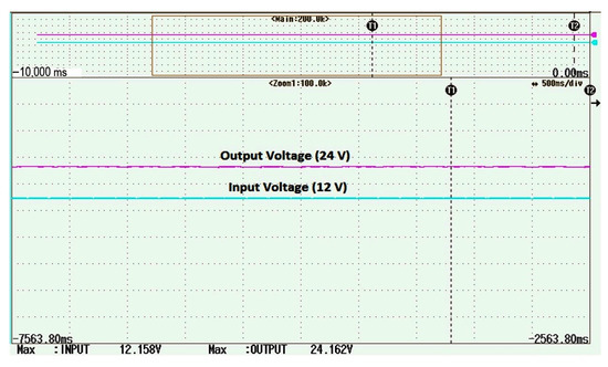
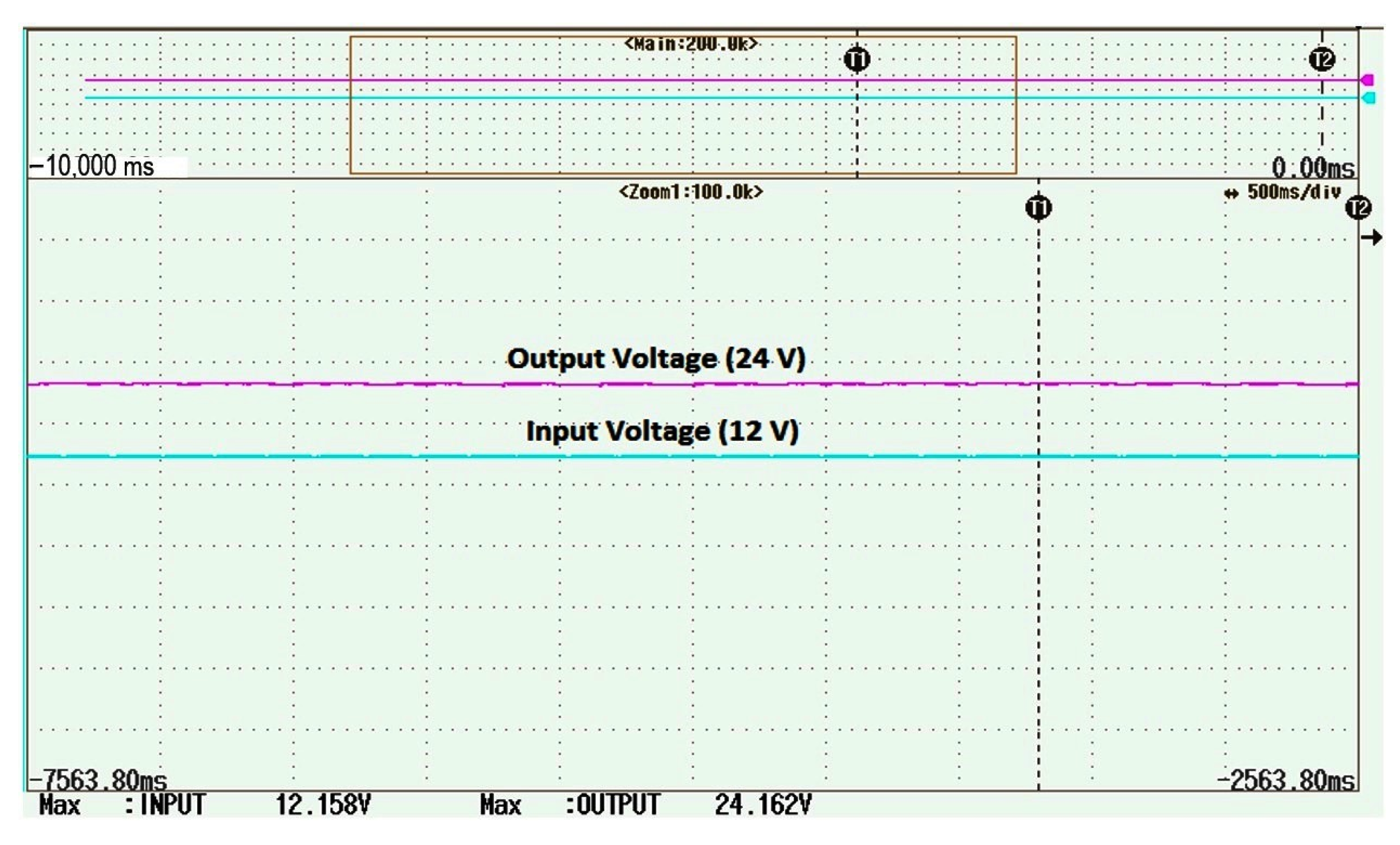
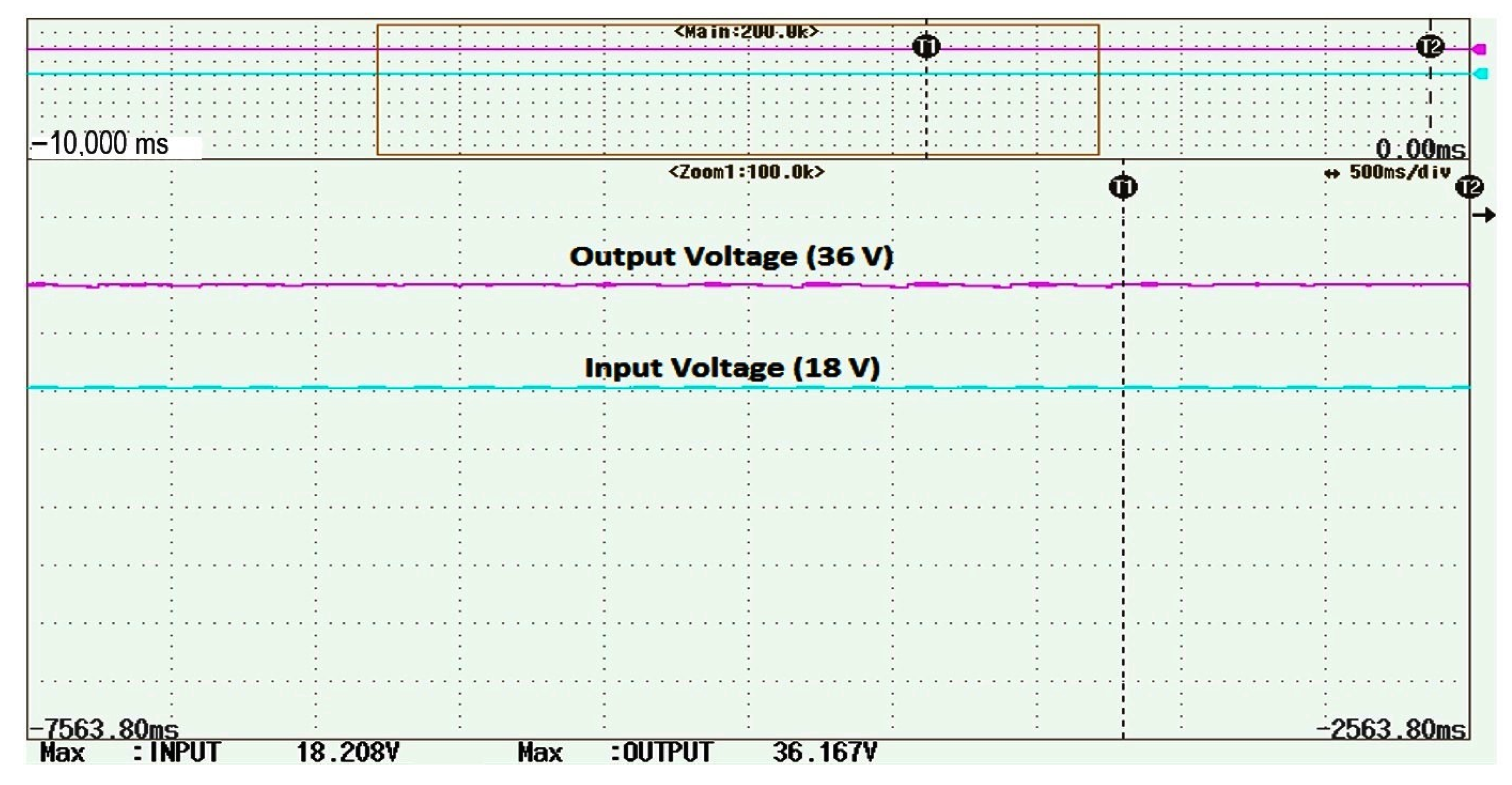
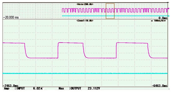
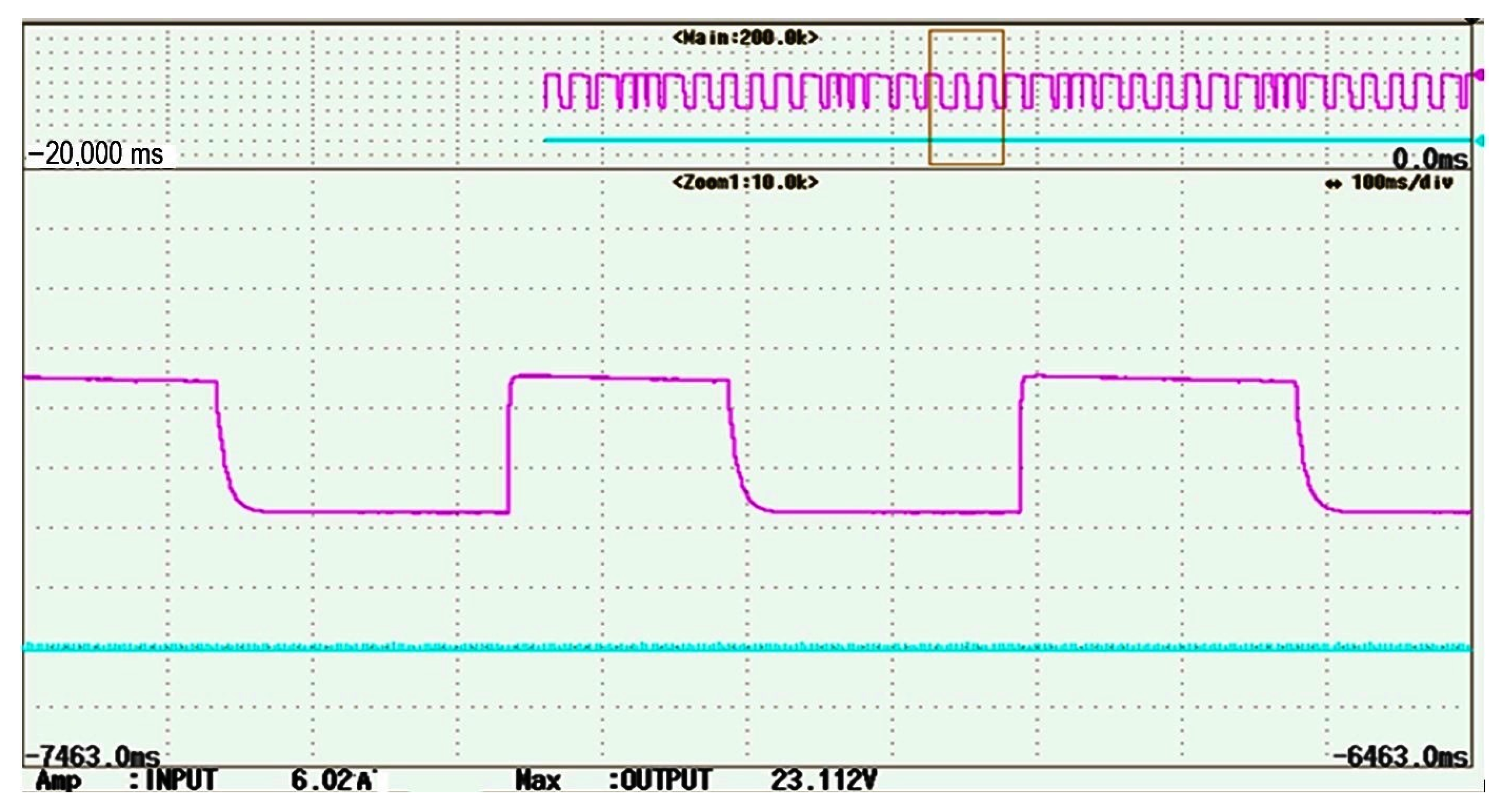
The converter was operated in both the forward and reverse modes to verify its bidirectional property. Switches S1 and S2 were alternatively triggered, while S3 and S4 were kept OFF and ON, respectively, to allow the converter operation in boost mode. The input and output voltage waveforms were recorded for both the forward and reverse modes and are depicted in Figure 18 and Figure 19, respectively. The input voltage was maintained at 12 V, and a 24 volt output was measured as seen in Figure 18 for forward mode of operation. A different input voltage of 18 volts was maintained as the input side for the reverse mode of operation, and a 36 volt output was measured as seen in Figure 19.
Figure 18.
Input and output voltage waveforms under forward mode of operation.
Figure 19.
Input and output voltage waveforms under reverse mode of operation.
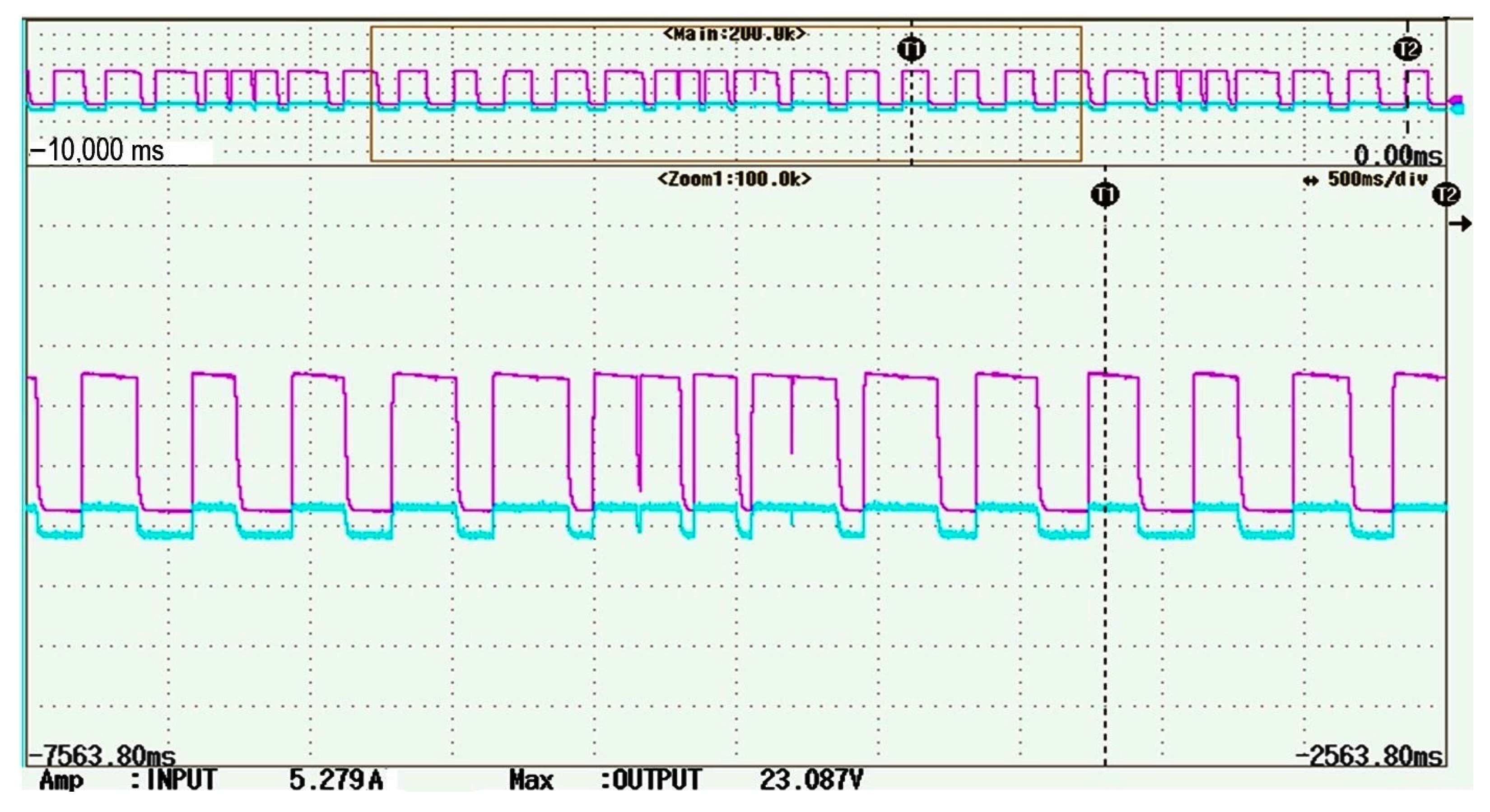
The input current and voltage waveforms under both forward and reverse modes of operation of the converter were also recorded and are presented in Figure 20 and Figure 21, respectively. The prototype of the split-pi converter was tested for half and full load conditions also, and the results show good matching with the simulation studies performed. The current ripples were less than 5%, and the voltage ripples were less than 2% in all loading conditions. The efficiency at the indicated voltages and currents is nearly 88.7%, and the temperatures reached by the power components after full load were only 2 degrees more than the ambient.
Figure 20.
Input current and voltage waveforms under forward mode of operation.
Figure 21.
Input current and voltage waveforms under reverse mode of operation.
5. Conclusions
In this paper, the steady-state modeling for different modes of operation of the SPC was studied in detail. A state–space averaging scheme was adopted to formulate the small-signal open-loop transfer functions of the input current and output voltage. The small-signal transfer functions were derived for both the boost and buck modes of operation of the converter. Sample case studies of compensator design for stable operation of the converter under various operating modes were presented. Frequency response plots were illustrated for both the uncompensated and compensated systems. An experimental prototype of the SPC with closed-loop control proving its bidirectional capability was developed, and the recorded results were presented.
Author Contributions
Conceptualization, G.S.; methodology, G.S.; software, G.S.; validation, G.S., V.K. and J.S.M.; formal analysis, V.K.; investigation, V.K.; resources, J.S.M.; data curation, J.S.M.; writing—original draft preparation, G.S.; writing—review and editing, V.K.; visualization, G.S.; supervision, V.K. All authors have read and agreed to the published version of the manuscript.
Funding
The research received no external funding.
Institutional Review Board Statement
The study did not require any ethical approval.
Informed Consent Statement
Not applicable.
Conflicts of Interest
The authors declare no conflict of interest.
References
- Bellur, M.; Kazimierczuk, M.K. DC–DC Converters for Electric Vehicle Applications. In Proceedings of the Electrical Insulation Conference and Electrical Manufacturing Expo, Nashville, TN, USA, 22–24 October 2007. [Google Scholar]
- Sangtaek, H.; Divan, D. Bi-directional DC/DC converters for plug-in hybrid electric vehicle (PHEV) applications. In Proceedings of the IEEE Applied Power Electronic Conference and Exposition, Austin, TX, USA, 24–28 February 2008; pp. 784–789. [Google Scholar]
- Wai, R.J.; Duan, R.Y.; Jheng, K.H. High-efficiency bidirectional DC–DC converter with high-voltage gain. IET Power Electron. 2012, 5, 173–184. [Google Scholar] [CrossRef] [Scilit]
- Rehman, Z.; Al-Bahadly, I.; Mukhopadhyay, S. Dual input-dual output single inductor DC–DC converter for renewable energy applications. In Proceedings of the International Conference on Renewable Energy Research and Applications, Yokohama, Japan, 9–12 November 2015; pp. 783–788. [Google Scholar]
- Anurag, M.B.; Thrinath, G.S.; Karanki, S.B.; Yallamili, R. Design of ZVS based high gain DC–DC converter for PV applications. In Proceedings of the IEEE International Conference on Renewable Energy Research and Applications, Birmingham, UK, 20–23 November 2016; pp. 584–589. [Google Scholar]
- Tytelmaier, K.; Husev, O.; Veligorskyi, O.; Yershov, R. A review of non-isolated bidirectional DC–DC converters for energy storage systems. In Proceedings of the 2016 II International Young Scientists Forum on Applied Physics and Engineering (YSF), Kharkiv, Ukraine, 10–14 October 2016; pp. 22–28. [Google Scholar]
- Mumtaz, F.; Yahaya, N.Z.; Meraj, S.T.; Singh, B.; Kannan, R.; Ibrahim, O. Review on non-isolated DC-DC converters and their control techniques for renewable energy applications. Ain Shams Eng. J. 2021, 12, 3747–3763. [Google Scholar] [CrossRef] [Scilit]
- Xue, F.; Yu, R.; Huang, A.Q. A 98.3% efficient gain isolated bidirectional DC–DC converter for DC microgrid energy storage system applications. IEEE Trans. Ind. Electron. 2017, 64, 9094–9103. [Google Scholar] [CrossRef] [Scilit]
- Chen, J.; Sha, D.; Yan, Y.; Liu, B.; Liao, X. Cascaded high voltage conversion ratio bidirectional non-isolated DC–DC converter with variable frequency control. IEEE Trans. Power Electron. 2017, 33, 1399–1409. [Google Scholar] [CrossRef] [Scilit]
- Gorji, S.A.; Sahebi, H.G.; Ektesabi, M.; Rad, A.B. Topologies and Control Schemes of Bidirectional DC–DC Power Converters: An Overview. IEEE Access 2019, 7, 117997–118019. [Google Scholar] [CrossRef] [Scilit]
- Chub, A.; Vinnikov, D.; Kosenko, R.; Liivik, E.; Galkin, I. Bidirectional DC–DC Converter for Modular Residential Battery Energy Storage Systems. IEEE Trans. Ind. Electron. 2020, 67, 1944–1955. [Google Scholar] [CrossRef] [Scilit]
- Odo, P. A Comparative Study of Single-phase Non-isolated Bidirectional DC–DC Converters Suitability for Energy Storage Application in a DC Microgrid. In Proceedings of the 2020 IEEE 11th International Symposium on Power Electronics for Distributed Generation Systems (PEDG), Dubrovnik, Croatia, 28 September–1 October 2020; pp. 391–396. [Google Scholar]
- Rajini, V.; Magdalene, A. Investigations on Interleaved and Coupled Split-Pi DC–DC Converter for Hybrid Electric Vehicle Applications. Int. J. Renew. Energy Res. 2021, 11, 808–817. [Google Scholar]
- Alzahrani, A.; Shamsi, P.; Ferdowsi, M. Single and interleaved split-pi DC–DC converter. In Proceedings of the 2017 IEEE 6th International Conference on Renewable Energy Research and Applications (ICRERA), San Diego, CA, USA, 5–8 November 2017; pp. 995–1000. [Google Scholar]
- Ahmad, T.; Sobhan, S. Performance analysis of bidirectional split-Pi converter integrated with passive ripple cancelling circuit. In Proceedings of the 2017 International Conference on Electrical, Computer and Communication Engineering (ECCE), Cox’s Bazar, Bangladesh, 16–18 February 2017; pp. 433–437. [Google Scholar]
- Karbivska, T.; Kozhushko, Y.; Nataraj Barath, J.G.; Bondarenko, O. Split-Pi Converter for resistance welding Application. In Proceedings of the 2020 IEEE KhPI Week on Advanced Technology (KhPI Week), Kharkiv, Ukraine, 5–10 October 2020; pp. 391–395. [Google Scholar] [CrossRef] [Scilit]
- Sobhan, S.; Bashar, K.L. A novel Split-Pi converter with high step-up ratio. In Proceedings of the 2017 IEEE Region 10 Humanitarian Technology Conference (R10-HTC), Dhaka, Bangladesh, 21–23 December 2017; pp. 255–258. [Google Scholar]
- Crocker, T.R. Power Converter and Method for Power Conversion. U.S. Patent 20040212357 A1, 28 October 2004. [Google Scholar]
- Singhal, M.; Pilli, N.K.; Singh, S.K. Modeling and analysis of split-Pi converter using State space averaging technique. In Proceedings of the 2014 IEEE International Conference on Power Electronics, Drives and Energy Systems (PEDES), Mumbai, India, 16–19 December 2014; pp. 1–6. [Google Scholar]
- Monteiro, V.; Oliveira, C.; Rodrigues, A.; Sousa, T.J.C.; Pedrosa, D.; Machado, L.; Afonso, J.L. A Novel Topology of Multilevel Bidirectional and Symmetrical Split-Pi Converter. In Proceedings of the 2020 IEEE 14th International Conference on Compatibility, Power Electronics and Power Engineering (CPE-POWERENG), Setubal, Portugal, 8–10 July 2020; pp. 511–516. [Google Scholar]
- Luna, M.; Sferlazza, A.; Accetta, A.; di Piazza, M.C.; la Tona, G.; Pucci, M. Modeling and Performance Assessment of the Split-Pi Used as a Storage Converter in All the Possible DC Microgrid Scenarios. Part I: Theoretical Analysis. Energies 2021, 14, 4902. [Google Scholar] [CrossRef] [Scilit]
- Maclaurin, A.; Okou, R.; Barendse, P.; Khan, M.A.; Pillay, P. Control of a Flywheel Energy Storage System for Rural Applications Using a Split-Pi DC–DC Converter. In Proceedings of the IEEE International electric Machines & Drives Conference, Niagara Falls, ON, Canada, 15–18 May 2011. [Google Scholar]
- Ang, S.; Oliva, A. Power-Switching Converters, 2nd ed.; CRC Press: Boca Raton, FL, USA, 2005. [Google Scholar]
- Jiao, W.; Gao, Y.; Yan, W.; Wu, S.; Gao, F.; Yang, X. Simulation Analysis of Totem Pole PFC Using Steady Error Free Quadratic Optimal PID Control. In Proceedings of the 2021 11th International Conference on Power and Energy Systems (ICPES), Shanghai, China, 18–20 December 2021; pp. 290–294. [Google Scholar]
- Çalışkan, A.C.; Kocaağa, E.; Kasnakoğlu, C. Average and Peak Current Mode Control Comparison for Full-Bridge Converter. In Proceedings of the 2021 8th International Conference on Electrical and Electronics Engineering (ICEEE), Antalya, Turkey, 9–11 April 2021; pp. 202–206. [Google Scholar]
- Venkataramana, S. Small Signal Modeling of Non-Isolated High Gain DC–DC converter. In Proceedings of the 2020 International Conference for Emerging Technology (INCET), Belgaum, India, 5–7 June 2020; pp. 1–5. [Google Scholar]
- Laddha, A.; Satyanarayana, N.; Vijayakumar, K. State-space Modeling for a 4-Port DC–DC Converter. In Proceedings of the 2019 National Power Electronics Conference (NPEC), Tiruchirappalli, India, 13–15 December 2019; pp. 1–6. [Google Scholar]

Publisher’s Note: MDPI stays neutral with regard to jurisdictional claims in published maps and institutional affiliations. |
© 2022 by the authors. Licensee MDPI, Basel, Switzerland. This article is an open access article distributed under the terms and conditions of the Creative Commons Attribution (CC BY) license (https://creativecommons.org/licenses/by/4.0/).