Article

Online Failure Diagnostic in Full-Bridge Module for Optimum Setup of an IGBT-Based Multilevel Inverter

by
Juan Carlos Iglesias-Rojas
*,
Erick Velázquez-Lozada
and
Roberto Baca-Arroyo
Instituto Politécnico Nacional—ESIME Zacatenco, Unidad Profesional Adolfo López Mateos, Alcaldía Gustavo A. Madero, Mexico City 07738, Mexico
*
Author to whom correspondence should be addressed.
Energies 2022, 15(14), 5203; https://doi.org/10.3390/en15145203
Submission received: 19 June 2022 / Revised: 12 July 2022 / Accepted: 14 July 2022 / Published: 18 July 2022

Abstract

:
An online failure diagnostic test is essential to ensure the robustness and reliability of high-powered systems. Furthermore, the overall design must comprise diagnostic strategies to detect in-service and high-powered module defects. This paper describes the critical failure mechanisms––cross-conduction, inductive avalanche, second turn-on, VS-undershoot, inrush current, and thermal runaway––that directly affect insulated gate bipolar transistor (IGBT) operation. The constructed inverter contains 18 transformer-based taps (six per phase); however, this work studied a single tap (IGBT-based full-bridge module) to understand the reasons for failure and the routes to mitigate them. Moreover, a cost-effective solution using the IR2127STRPBF driver circuit was implemented to reduce the probability of thermal runaway in case of overcurrent, short-circuit, or avalanche events. For this reason, the electrical current state was adjusted using an FPGA digital resource to perform dynamic PWM control signals. The obtained correlation waveforms are valuable for verifying diagnostic data at the design stage to emphasize the significance of evading premature failure events. The comprehensive study on failure diagnosis enabled successful design strategies to construct a robust 45 kVA three-phase multilevel inverter for a 22 kW eolic-photovoltaic generation plant.

1. Introduction

Multilevel inverters (MLIs) have become more popular than conventional DC/AC inverters for some application fields because they operate with many voltage steps that improve the output waveform. They are categorized into non-isolated and isolated multilevel inverters, which are widely used in renewable energy systems and industrial applications, among others. Isolated MLIs exploit low-frequency transformers to improve robustness and reliability and are subcategorized into DC-side and AC-side. The MLIs feature several advantages over conventional topologies. MLIs operate at both high and low frequencies, reducing the device-switching rate; feature low-output harmonic distortion; achieve a high-power capability by dividing the total power into several switching devices; and extend the switching device’s lifetime and reliability due to low switching rates. Low-frequency MLIs reduce switching losses considerably, thereby enhancing overall efficiency. An extensive comparison among multilevel topologies (state of the art) elaborates on [1].
In this work, the low-frequency transformer plays a critical role at the design stage. Its electrical properties, such as high inductance, high inrush current, reduced di/dt, and high efficiency at heavy loads, determine several design techniques to prevent failure [2,3,4]. In addition, the full-bridge module sets up two arms that contain two isolated gate bipolar transistor (IGBT) devices. In any situation, one IGBT within an arm is solely on-state. However, when both IGBTs are on-state in a failure scenario, the current through the IGBT devices abruptly increases. This current is, in most cases, high enough to instantly damage the switching devices. In addition, the enormous di/dt may damage the IGBT and driver circuit, as seen in Figure 1. This failure mechanism is called a “type I” short-circuit event. However, if the event comes from the transformer output, the current flows through the transformer primary winding, reducing the di/dt considerably in the IGBT devices. A reduced di/dt enables a higher time window within the IGBT that must be turned off before firing. This failure scenario, which originated externally, is called a “type II” short-circuit event, which has a higher occurrence probability than type I. Figure 1 illustrates these possible short-circuit scenarios. Here, the circuit design must consider both failure events to prevent IGBT damage by turning it off immediately.
This work focuses on online failure diagnostics in AC-side isolated inverters, especially the cascade transformer multilevel inverter (CTMI). The inverter is part of an overall project of sustainable energy generation and distribution within a region where electric power lines are unavailable. The energy generation plant consists of a 12 kW solar panel generator, a 10 kW wind turbine, a 240 V-435 Ah battery bank, an isolated 45 kVA three-phase multilevel inverter, and a power distribution box.
The full-bridge module design is critical for the optimum performance of an energy generation plant. The failure mechanisms in the IGBT-based full-bridge module, such as cross-conduction, inductive load avalanche, second turn-on, VS-undershoot, and thermal runaway, will be described in Section 2. Measurements of the online failure mechanisms in a single-power stage (one full-bridge module) will be covered in Section 3. Section 4 discusses the transformer’s influence on current conduction and IGBT operating temperature when a driver circuit is used for online diagnostic as a function of the electrical current state. Using pulse width modulation (PWM) in a field programming gate array (FPGA) will also be detailed in this section. Finally, the conclusion is presented in Section 5.

2. Failure Mechanisms and Operation of a Full-Bridge Module

CTMIs are extensively used in large solar power plants because they feature low harmonic distortion, galvanic isolation, and low-frequency switching operation [5]. Moreover, CTMIs can improve reliability, robustness, and efficiency, despite the use of low-frequency transformers with high inductance [6,7,8,9]. More importantly, using a DC source solely has been cited as a CTMI advantage. The main disadvantage, however, is that it requires large transformers, which implies increased weight and inverter size.
As shown in Figure 1, the modular CTMI topology involves two types of short circuits. Short-circuit type I occurs when the current travels across a single arm of the full-bridge, whereas type II occurs when the current passes through the transformer’s primary winding. Several techniques to prevent IGBT failures have been published, e.g., [10]. However, many of these techniques are difficult to apply; moreover, they are not fully developed. The key critical failure mechanisms found on each full-bridge module incorporated at the CTMI are discussed below:
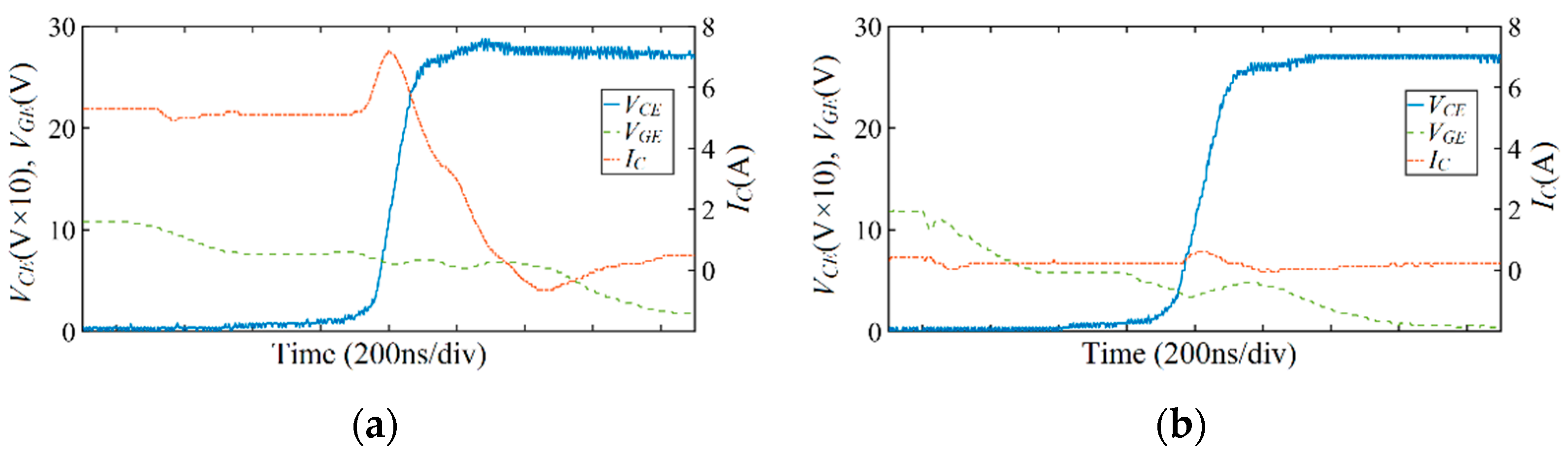
  • The cross-conduction mechanism emerges during the switching intervals while two IGBTs of the same arm are active. It means an IGBT turns on while the opposite IGBT has not yet turned off. Higher IGBT turn-off times and the driver propagation delays originate from this phenomenon. The cross-conduction is directly related to the switching losses; the higher the cross-conduction, the higher the loss. Furthermore, excessive cross-conduction produces high collector current spikes during transitions that gradually degrade the switching device. IGBT degradation leads to failures such as bonding-wire cracking and detachment, die stresses, and in some cases thermal breakdown.
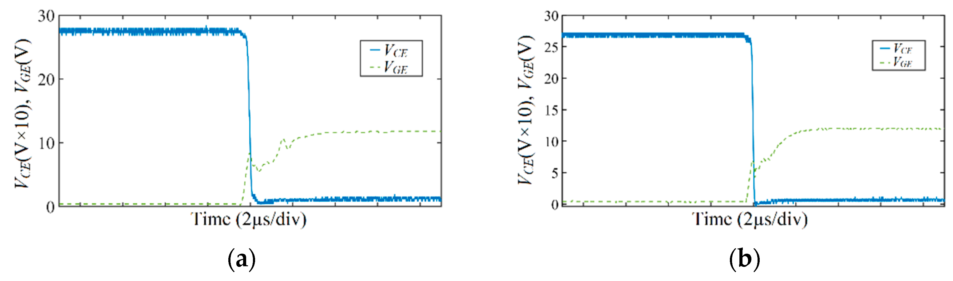
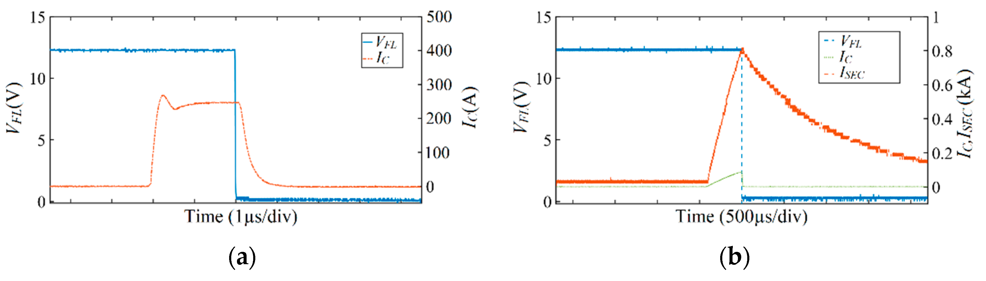
  • In high-inductance switching applications, managing the inductor-stored energy properly is a challenge nowadays. This stored energy becomes a high voltage spike that appears during the IGBT turn-off transition, causing an inductive load avalanche failure. The avalanche mechanism deals with the energy in a different way than a short-circuit does. In a short-circuit event, the IGBT is active, whereas in the avalanche event, the IGBT is gate-emitter voltage (VGE) unbiased.
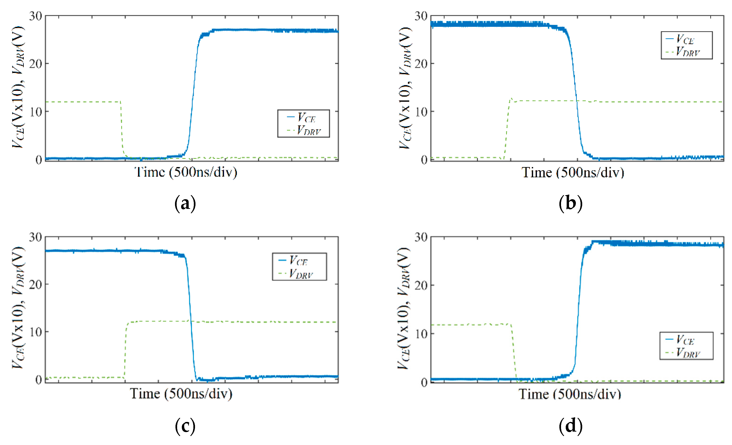
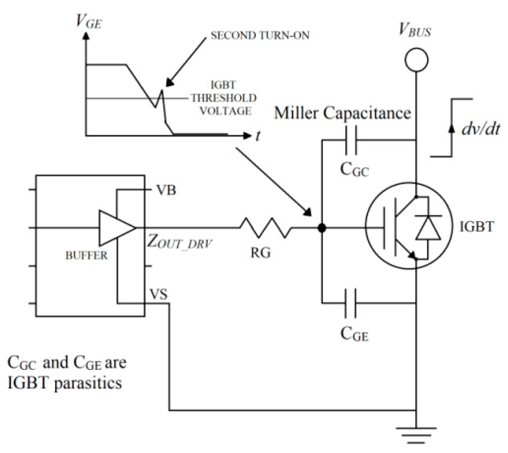
  • The second turn-on is a failure mechanism originated by the IGBT’s Miller capacitance combined with a high dv/dt at the collector node and leads to a type I short-circuit failure. This mechanism occurs when the high voltage at the collector node induces a voltage spike in the gate node during the IGBT turn-off transition. If the voltage spike reaches the IGBT plateau level, the device will turn on again. In addition, the induced voltage in the gate node may increase enough to reach the plateau level, turning on the IGBT, see Figure 2.
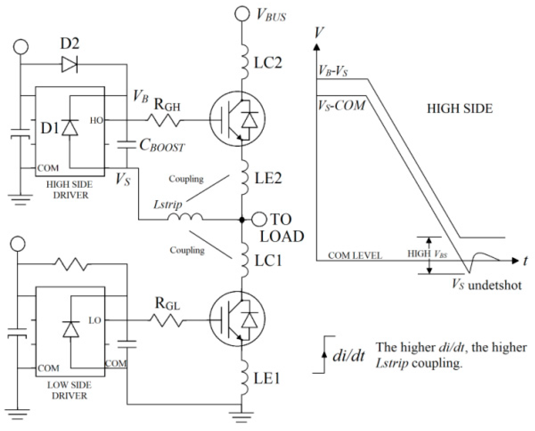
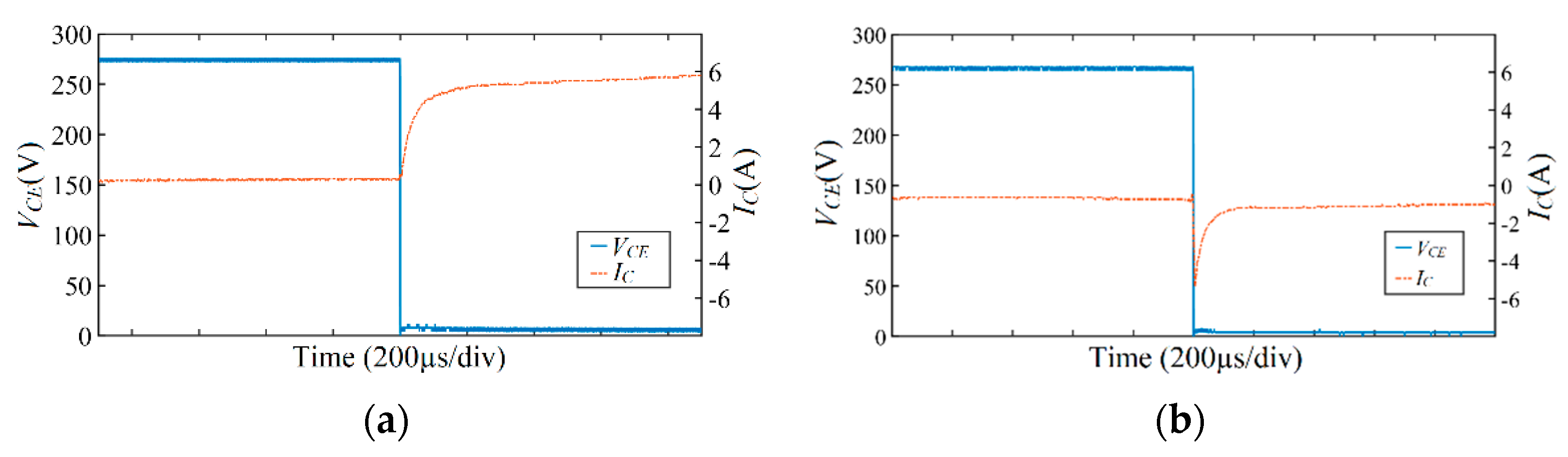
  • The VS-undershoot failure mechanism is an under-voltage spike that appears at the driver’s VS terminal, which is used for IGBT switching. When a high di/dt transition occurs, it is generated by the stored energy in the parasitic inductances of the collector and emitter IGBT terminals of the PCB tracks (Lstray). Therefore, VS-undershoot directly affects the high-side IGBT driver, as seen in Figure 3.
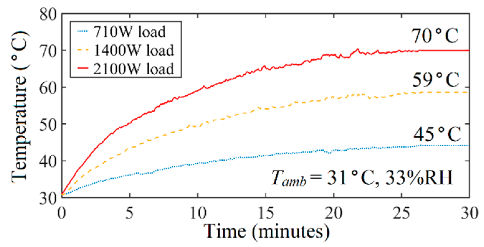
  • Thermal runaway is a failure mechanism that occurs when a rising temperature causes a further increase in temperature in each IGBT in the full-bridge module. Therefore, uncontrolled temperature-positive feedback leads the IGBT to a destructive scenario.
Figure 4 presents a constructed 45 kVA AC-side-isolated multilevel inverter block diagram. It shows a modular CTMI of 18 transformer-isolated power modules, FPGA-based control signal processing, microcontroller-based analog signal processing, human machine interface (HMI), analog front-end, DC main switch and protections, control-signal isolation module, isolated low-voltage power supplies, voltage and current sensors, DC-link, and control signals distribution. A single power stage called “single tap” is equivalent to the full-bridge module and comprises four IGBTs and a 2.5 kVA low-frequency transformer (see Figure 1). Here, failure mechanisms come from this module.
Previous literature has revealed several design techniques to detect short-circuit events. For example, conducting power semiconductor transistors, such as the metal oxide semiconductor field effect transistor (MOSFET), turn off quickly by adding a current-sensing circuit into the drain terminal [11]. This technology has advantages over the conventional shunt method because it does not directly affect the load voltage. Nevertheless, these special switching devices are not widely available commercially.
A short-circuit detection method based on current shunts built into an IGBT power module that effectively reduces the IGBT turn-off time upon a short-circuit event has been introduced [12]. However, that method uses shunt resistors that require additional circuit stages, such as an RC compensation circuit and a filtered amplifier. Other methods use di/dt and dv/dt detection to infer a short-circuit event [13,14]. Nonetheless, these methods require complex hardware. Finally, another method analyses the IGBT gate voltage to detect hard switching faults and faults under load [15]; the IGBT driver hardware is significantly more complex.
This authors of this manuscript prefer conventional IGBT desaturation to previous methods for online diagnostic short-circuit events for its robustness, well-known trade-offs, and commercial availability of the IGBT driver. However, the IGBT desaturation technique involves a significant IGBT turn-off time on a short-circuit event. This is called the “blanking time (tb)”, which depends on a passive integrator RC constant and a propagation delay of each implemented IGBT driver circuit. A large tb combined with a high desaturation current could lead to an IGBT thermal breakdown. References [16,17,18,19] explain how to improve the desaturation technique by reducing tb even if the IGBT operates with high currents. Therefore, it determines the short-circuit time that the IGBT must withstand. Figure 5 depicts the main components of the fabricated full-bridge module (single tap). The critical design specifications are listed in Table 1.

3. Online Diagnostic of the Failure Mechanisms

The circuit design proposed here for the online diagnostic of failure mechanisms due to short-circuit events improves on the one proposed in [20]. Figure 6 depicts the enhanced design of the high-side driver solely. The principal changes comprise the driver substitution by the IR2127STRPBF integrated circuit, the gate voltage clamp, the VS-undershoot reduction resistor (R4), and the use of a short-circuit tolerant IGBT.
According to [21], R2 is typically chosen to be 10 k for a bootstrap voltage VB = 12 V, 22 k for VB = 15 V and 33 k for VB = 18 V. The voltage VX is typically 9.2. All the component values of the proposed circuit are listed in Table 2. These components are jointly optimized to achieve stable performance across the operation conditions. This optimization was performed by several trade-offs of the relevant component values as follows:
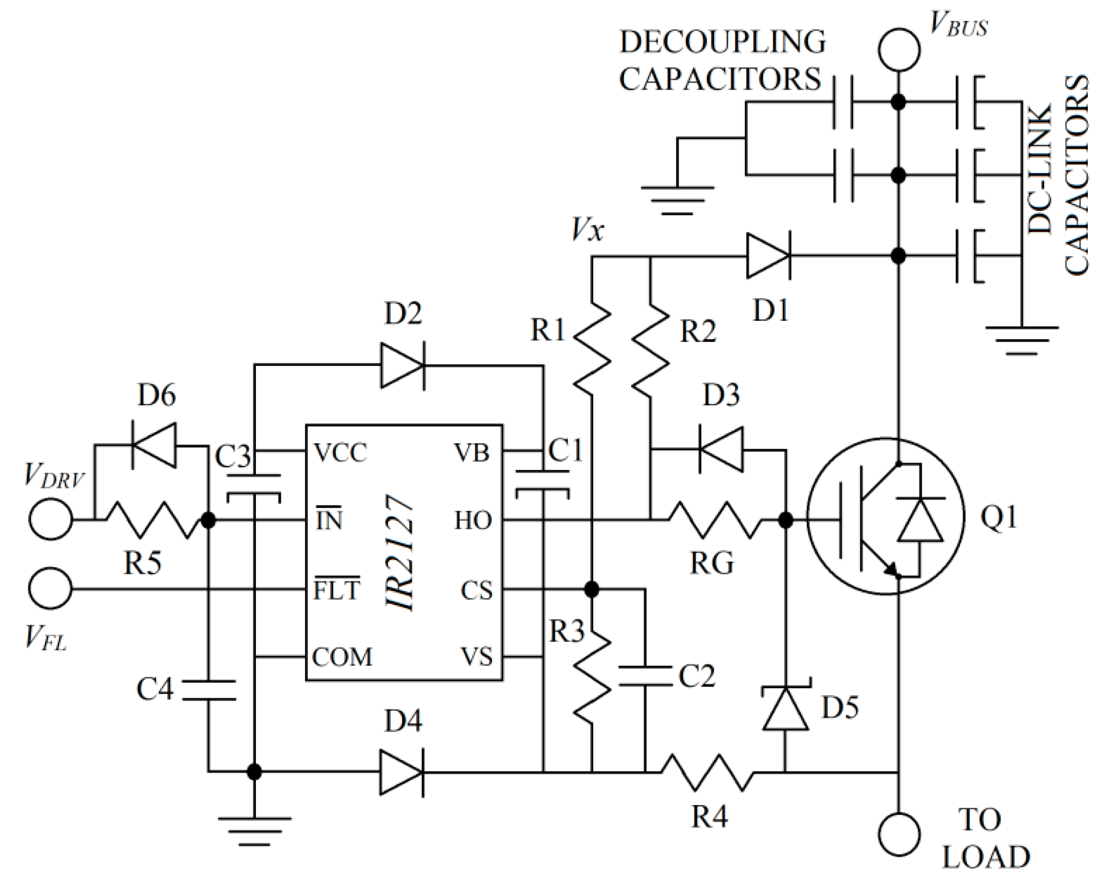
  • R1, R2, R3, and C2 values established the driver shutdown delay to prevent an unstable failure condition during the IGBT turn-on time. Therefore, the minimum shutdown delay was the IGBT turn-on time, and the maximum was the IGBT short-circuit withstanding time minus the driver shutdown propagation delay. The optimum shutdown delay should be slightly higher than the IGBT turn-on time.
  • The RG value predominantly sets the gate impedance, which should be as low as possible to reduce the probability of the second turn-on phenomenon. However, the RG also creates a delay path to increase the IGBT turn-on time, preventing cross-conduction failure. Moreover, it slightly increases dv/dt, reducing the harmful effects of the Miller capacitance. The optimum RG value is the one that equals the IGBT turn-on and turn-off times.
  • The boost capacitor C1 stores the energy to keep the high-side IGBT active when needed. Its value is essential, especially in low-frequency applications. C1 also plays an essential role in setting the driver’s output impedance during the high logical state. In Section 3.3, detailed information on the C1 optimum value calculation is presented.
The circuit in Figure 6 sets up R1, R2, R3, C2, D1, and the IR2127STRPBF driver to accomplish the online diagnostic on the current signal. The operation principle is based on the statement that a saturated IGBT (Q1) increases its collector-emitter voltage (VCE) as the collector current increases. The higher the IC, the higher the VCE. The IGBT driver uses a current sense (CS) terminal to detect an IC increase by reading the VCE voltage.
When Q1 is inactive, IC is close to zero, and VCE equals the DC-link power supply voltage (VBUS). At this stage, D1 isolates the collector voltage of the voltage divider built with R1 and R3. The HO terminal remains low; thus, CS voltage goes below the threshold voltage VCSth [22], determining a regular operation. If the HO terminal asserts that VCE remains equal to VBUS until the turn-on time elapses, the CS voltage gradually increases due to the integrator action of R1, R2, R3, and C2. CS voltage must not reach VCSth before VCE goes down to prevent an erratic short-circuit event. However, when VCE finally goes down, D1 becomes active and establishes a VCSVS voltage below VCSth.
If a short-circuit event occurs while Q1 is active, VCE increases to a value determined by the desaturation current and the VGE voltage [23]; therefore, D1 is reverse-biased and isolates the CS voltage divider of the collector voltage. As the HO terminal stills asserted, CS starts rising again until it reaches VCSth. At this point, the CS signal is propagated into the driver until the HO signal shutdowns the IGBT and the FAULT terminal is driven low, indicating a short-circuit failure event.
After building the improved IR2127STRPBF driver, it was implemented into the power board as shown in Figure 5, and an IGBT-based multilevel inverter module was tested.
Figure 7 shows the measurement setup, where all measurements were taken in the laboratory under fault-tolerant scenarios. Three 700 W resistive loads, a Xilinx Zynq-7000 FPGA board, an isolation interface between the FPGA and the power board, and a 2.5 kVA low-frequency transformer were used as the testbench. Furthermore, a 10 kVA three-phase multi-tap isolation transformer for security purposes was also used.
Failure-event measurement on the IGBT-based full-bridge inverter (single tap) was performed and evaluated by correlation plots of the electrical parameters. These measurements required a digital-storage oscilloscope type Siglent SDS-1102CML (Siglent Technologies, Shenzhen, China) with low-capacitance probes (model P6120: Tektronics Inc., Beaverton, OR, USA). Current values were measured using an AC clamp (model i400s: Fluke Corporation., WA, USA), Magneto-resistor current sensor (model DS10.2s: Tell-i Technologies Inc., Charlotte, NC, USA), and a 1000 A bidirectional current sensor (model SSA-1000: Riedon Resistors., Alhambra, CA, USA) and measured when connected to a Siglent SDS-1102CML oscilloscope (see Figure 7).
A technical description related to each failure mechanism evaluated in the “power board” is given below.

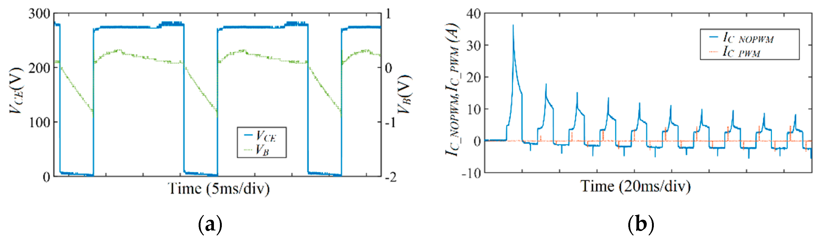
3.1. Cross-Conduction

Since the low-side IGBTs of the full-bridge module also operate as clamping devices for the high-inductive load of the transformer’s primary winding, it is necessary to keep a certain level of cross-conduction to prevent an unclamped high-inductive scenario. A good trade-off equals the IGBT turn-on and turn-off times. Passive delay lines equal the switching times to achieve a good balance between switching losses and unclamped high inductive spikes (UIS). For example, RG, D3, R5, C4, and D6 from Table 2 set up two delay lines to control cross-conduction. Figure 8 shows the experimental results from measuring the low-side and high-side switching times. After the passive-delay lines design, turn-on and turn-off times are almost equal.
Figure 9a depicts the high-side VCE and IC, waveforms. Notice that the IGBT lies within the safe operating area (SOA) where cross-conduction does not visually influence the collector current, and VCE does not present high-voltage spikes due to UIS. Figure 9b shows the low-side VCE and IC waveforms. The low-side turn-on transition lies within the clamping stage of the transformer’s primary winding inductance. However, a slightly negative clamping current spike was observed.

3.2. Inductive Avalanche

Under this condition, the current distribution across the surface of the IGBT die was uniform, maximizing the ability to dissipate the energy. In the avalanche event, the IGBT was non-conducting with no bias on the gate. Thus, when an avalanche occurred, the current travelled around the perimeter of the die, creating a non-uniform current distribution across its surface, so the maximum current for failure was much less in the avalanche event than in the short-circuit event [24,25].
Because of high transformer inductance, several precautions had be taken: (1) dv/dt was limited by increasing the RG value. This change did not affect conduction losses as VGE did; (2) A certain level of cross-conduction was permitted; however, the optimum cross-conduction time was zero; (3) switching coding was used to let the inductive load clamp through the low-side IGBTs; (4) the printed circuit board (PCB) parasitic inductances (Lstray) were reduced (5) The equivalent series resistance (ESR) and equivalent series inductance (ESL) of the DC-link capacitors were reduced. As seen previously, dv/dt was reduced. Notice that the low switching frequency operation did not influence efficiency because of switching loss. According to [26], dv/dt was limited by physical parameters, such as threshold gate voltage (VTH), total gate resistance (RG), and gate-emitter capacitance (CGC). Thus, the ESR was reduced by paralleling low ESR capacitors as closely as possible to the IGBTs.
Measurements of VCE, IC, and VGE were taken during the IGBTs turn-off transition of high- and low-side IGBTs accordingly. Figure 10a shows the VCE, IC, and VGE waveforms during the turn-off transition of the high-side IGBT. Notice that VCE did not observe voltage spikes, and the IGBT tail current was disclosed. Figure 10b shows the VCE, IC, and VGE waveforms during the turn-off transition of the low-side IGBT. Again, VCE transition did not present spikes from the clamping process implemented by programming. Again, the low-side IGBT turn-off transition occurred during the clamping time, so no further IC transition was observed.

3.3. Second Turn-On

Gate–node impedance and dv/dt strongly influenced the gate-emitter voltage; therefore, voltage induction was reduced by adding an external capacitor between the gate and emitter nodes [27]. Gate impedance was reduced by paralleling an ultra-fast-recovery diode to RG. As a result, RG was obtained according to [28] and equaled 10 Ω.
Figure 11 presents the influence of dv/dt during the turn-on transition. Its influence on VGE was also seen during the turn-on transition, thus avoiding the risk of causing a second turn-on event due to induced spikes through the scope probes. After decreasing gate impedance, a small influence was observed, and VGE was poorly affected by dv/dt.

3.4. VS-Undershoot

Since CTMIs use low-frequency transformers that limit di/dt, one would think that VS-undershoot could be neglected. However, during a short-circuit event or an overload condition, the Lstray current could be high enough to undershoot the VS terminal. Thus, the high-side driver could fail. Reference [29] suggests some general recommendations to minimize VS-undershoot: (1) use a thick, direct track between switches to avoid loops or deviations; (2) avoid interconnect links; (3) consider re-locating IGBTs to reduce track lengths; (4) connect VS and COM as close as possible to the IGBT pins; (5) locate the driver as close as possible to the IGBTs; (6) increase the bootstrap capacitance using low-ESR capacitors; (7) use a second low-ESR capacitor from VCC to COM; (8) add a resistor R4 from COM to the IGBT emitter; and (9) add a fast recovery diode D4 from COM to VS, as shown in Figure 6. Here, the VS-undershoot severity is measured as the difference between (VBVS) − (VS − COM) under overload or short-circuit conditions.
Figure 12 shows the VS-undershoot phenomenon under an overload condition. Isolated probes were required to accomplish this measurement. The condition met the following parameters: power = 3.52 kVA; transformer secondary winding current ISEC = 176.3 A; overload rate = 150%; and room temperature = 31 °C, respectively. The VS-undershoot severity was neglected after following the previous recommendations. Furthermore, the VS-undershoot directly affected the high-side driver leading to a latch-up failure.

3.5. Thermal Runaway

A method to predict the IGBT junction temperature and negative impact of high temperature on the die solder joints is introduced in [30]. A high collector current mainly causes thermal runaway during turn-off transition [31]; therefore, the following design considerations should be taken to prevent this condition: (1) Limit the short-circuit current by decreasing VGE but not so much that it causes excessive power losses, increasing the device temperature; (2) Reduce the short-circuit “blanking time (tb)” as much as possible; (3) Keep VB ripple voltage as low as possible by installing a bootstrap capacitor; (4) Maintain the IGBT case temperature as low as possible by using a robust thermal management system. Thermal management was not described in this paper; however, the results included IGBT temperature under several load conditions. Figure 13 presents three conditions when the IGBTs were mounted on a 180 × 130 × 33 mm aluminum heat sink without force convection. In addition, the average temperature of the four IGBT cases was reported.

4. Discussion

In low-frequency switching applications, a high transformer inrush current at the start may affect the DC-link voltage, leading to an input voltage failure, and the bootstrap capacitor in the driver circuit IR2127STRPBF plays a critical role in full-bridge module efficiency. Under this scenario, conductive losses were higher than switching losses because large power transformers featured nonlinear core magnetization, and a relatively low VGE implied a higher VCE, increasing IGBT temperature.
The modular CMIs contain several transformers, so the total inrush current drawn from the DC-link was the sum of each transformer’s particular inrush current. As a result, a huge current drawn from the DC-link led to failure due to a transient voltage drop. Indeed, a good selection of DC-link capacitors is central to preventing design drawbacks, and large bootstrap capacitors are required to prevent a considerable voltage drop in VGE during conduction to keep ripple voltage VB as low as possible [32].
Figure 14 shows a dynamic correlation between inrush current and voltage drop at the IGBT’s collector terminal when a 47 µF low-ESR bootstrap capacitor was used. For this purpose, a tantalum capacitor was connected in parallel with a ceramic capacitor. The PWM technique at the inverter startup considerably reduced the inrush current to prevent DC-link failure. Figure 14 also includes the transformer’s inrush current waveform without a PWM soft-start process.
The IGBT in the full-bridge module can withstand a collector current of 300 A during the blanking time without suffering failure. The maximum collector current was controlled, and the short-circuit current was limited mainly by VGE. An excessive collector current during turn-off can lead the IGBT to either a latch-up mechanism failure or thermal runaway when a higher IC and VGE nominal value is 13 V. In any case, the IGBT would be destroyed.
Likewise, a reduced di/dt can be observed due to the high inductance of the transformer’s primary winding. Here, the collector current was restricted by VGE and the CS voltage divider in the IR2127 driver. Thus, the designer had to ensure that the product of VCE and IC during desaturation lay within the safe operating area (SOA).
Figure 15a shows the fault terminal voltage (VFL) when a high di/dt short-circuit failure mechanism occur, and that the total blanking time after the IGBT shutdown process began was around 2 µs. Figure 15b shows the short-circuit failure mechanism when the transformer secondary winding current (ISEC) caused a short-circuit around 800 A, whereas the transformer primary winding inductance limited di/dt. In this case, the blanking time resulted in 470 µs for a VGE = 13 V.
Additionally, Table 3 resumes some critical features of this work compared with recent research for improving IGBT performance.

5. Conclusions

The measurements focused on online failure detection when an isolated full-bridge inverter module operated for more than 20 months under adverse conditions confirmed that this research project had a reliable and robust design. By using two passive delay lines inserted into the control signals path to prevent cross-conduction successful failure-event reduction was achieved because of a meticulous design trade-off between cross-conduction and proper transformer inductance energy deviation, which prevented an inductive load avalanche. Furthermore, a low IGBT gate impedance prevented a second turn-on occurrence because of the Miller capacitance and high dv/dt. Proper PCB design techniques lowered the VS-undershoot caused by parasitic inductances of the collector and emitter IGBT terminal paths. We also showed the importance of thermal management because a relatively low IGBT package temperature reduces the probability of thermal runaway in case of overcurrent, short-circuit, or avalanche events. Hence, online failure diagnostics solved by using cost-effective integrated circuits can ensure an efficient, reliable, and robust operation of high power systems under critical failure events.

Author Contributions

J.C.I.-R. planned the research topic and experimental development. E.V.-L. analyzed the results from collected data. R.B.-A. wrote and revised the manuscript. All authors have read and agreed to the published version of the manuscript.

Funding

This research received no external funding and the APC was funded by the authors.

Institutional Review Board Statement

Not applicable.

Informed Consent Statement

Not applicable.

Data Availability Statement

Not applicable.

Conflicts of Interest

The authors declare no conflict of interest.

References

  1. Hassan, A.; Yang, X.; Chen, W.; Houran, M.A. A State of the Art of the Multilevel Inverters with Reduced Count Components. Electronics 2020, 9, 1924. [Google Scholar] [CrossRef]
  2. Daher, S.; Schmid, J.; Antunes, F.L.M. Multilevel Inverter Topologies for Stand-Alone PV Systems. IEEE Trans. Ind. Electron. 2008, 55, 2703–2712. [Google Scholar] [CrossRef]
  3. Bukhari, S.S.H.; Atiq, S.; Kwon, B.-I. Elimination of the Inrush Current Phenomenon Associated with Single-Phase Offline UPS Systems. Energies 2016, 9, 96. [Google Scholar] [CrossRef] [Green Version]
  4. Dodge, J.; Hess, J. IGBT Tutorial. Application Note APT0201. 2002. Available online: www.academia.edu/9345985/ApplicationNoteAPT0201RevIGBTTutorial (accessed on 1 April 2022).
  5. Verdugo, C.; Candela, J.I.; Rodriguez, P. Energy Balancing with Wide Range Operation in the Isolated Multi-Modular Converter. IEEE Power Energy Soc. Section. 2020, 8, 84479–84489. [Google Scholar] [CrossRef]
  6. Gandomi, A.A.; Saeidabadi, S.; Hossein, S.; Babaei, E.; Gandomi, Y.A. Flexible Transformer Based Multilevel Inverter Topologies. IET Power Electron. 2018, 12, 578–587. [Google Scholar] [CrossRef]
  7. Behara, S.; Sandeep, N.; Yaragatti, U.R. Design and Implementation of Transformer-Based Multilevel Inverter Topology With Reduced Components. IEEE Trans. Ind. Appl. 2018, 54, 4632–4639. [Google Scholar] [CrossRef]
  8. Salehahari, S.; Babaei, E.; Hossein, S.; Ajami, A. Transformer-Based Multilevel Inverter: Analysis, design and implementation. IET Power Electron. 2018, 12, 1–10. [Google Scholar] [CrossRef]
  9. Panda, A.; Suresh, Y. Performance of Cascaded Multilevel Inverter by Employing Single and Three-Phase Transformers. IET Power Electron. 2012, 5, 1694–1705. [Google Scholar] [CrossRef]
  10. Choi, U.-M.; Blaabjerg, F.; Lee, K.-B. Study and Handling Methods of Power IGBT Module Failures in Power Electronic Converter Systems. IEEE Trans. Power Electron. 2014, 30, 2517–2533. [Google Scholar] [CrossRef]
  11. ON Semiconductor. Current Sensing Power MOSFETs. AND8093/D. 2017. Available online: www.onsemi.com/pub/Collateral/AND8093-D.PDF (accessed on 1 April 2022).
  12. Meng, Z.; Yang, Y.; Gao, Y.; Ai, S.; Fang, Z.; Wen, Y.; Wu, L. A Novel IC Measurement Without Blanking Time for Short-Circuit Protection of High-Power IPM. IEEE Access 2020, 8, 64475–64485. [Google Scholar] [CrossRef]
  13. Shu, L.; Zhang, J.; Shao, S. Crosstalk Analysis and Suppression for a Closed-Loop Active IGBT Gate Driver. IEEE J. Emerg. Sel. Top. Power Electron. 2018, 7, 1931–1940. [Google Scholar] [CrossRef]
  14. Groeger, J.; Schindler, A.; Wicht, B.; Norling, K. Optimized dv/dt, di/dt Sensing for a Digitally Controlled Slope Shaping Gate Driver. In Proceedings of the 2017 IEEE Applied Power Electronics Conference and Exposition (APEC), Tampa, FL, USA, 26–30 March 2017. [Google Scholar] [CrossRef]
  15. Li, X.; Xu, D.; Zhu, H.; Cheng, X.; Yu, Y.; Ng, W.T. Indirect IGBT Over-Current Detection Technique Via Gate Voltage Monitoring and Analysis. IEEE Trans. Power Electron. 2018, 34, 3615–3622. [Google Scholar] [CrossRef]
  16. Hain, S.; Bakran, M. The Benefit of Using an IGBT with a High Desaturation Current. In Proceedings of the 2017 19th European Conference on Power Electronics and Applications (EPE’17 ECCE Europe), Warsaw, Poland, 11–14 September 2017. [Google Scholar]
  17. Chen, M.; Xu, D.; Zhang, X.; Zhu, N.; Wu, J.; Rajashekara, K. An Improved IGBT Short-Circuit Protection Method with Self-Adaptive Blanking Circuit Based on VCE Measurement. IEEE Trans. Power Electron. 2018, 33, 6126–6136. [Google Scholar] [CrossRef]
  18. Yin, S.; Wu, Y.; Liu, Y.; Pan, X. Comparative Design of Gate Drivers with Short-Circuit Protection Scheme for SiC MOSFET and Si IGBT. Energies 2019, 12, 4546. [Google Scholar] [CrossRef] [Green Version]
  19. Krone, T.; Xu, C.; Mertens, A. Fast and Easily Implementable Detection Circuits for Short Circuits of Power Semiconductors. IEEE Trans. Ind. Appl. 2016, 53, 2871–2879. [Google Scholar] [CrossRef]
  20. Chokhawala, R.; Catt, J.; Kiraly, L. A discussion on IGBT short-circuit behavior and fault protection schemes. IEEE Trans. Ind. Appl. 1995, 31, 256–263. [Google Scholar] [CrossRef]
  21. Adams, J. Using the Current Sensing IR212X Gate Drive ICs. Application Note AN-1014. Available online: www.all-electronics.de/migrated/document/411pdf-an-1014 (accessed on 5 May 2022).
  22. International Rectifier. IR2127; Data Sheet. 2004. Available online: https://www.infineon.com/dgdl/Infineon-ir2127-DS-v01_00-EN.pdf?fileId=5546d462533600a4015355c868861696 (accessed on 8 May 2022).
  23. ON Semiconductor. NGTB50N120FL2W. 2015. Available online: www.onsemi.com/pdf/datasheet/ngtb50n120fl2w-d.pdf (accessed on 12 May 2022).
  24. Shen, C.; Hefner, A.R., Jr.; Berning, D.W.; Bernstein, J.B. Failure Dynamics of the IGBT During Turn-Off for Unclamped Inductive Loading Conditions. IEEE Trans. Ind. Appl. 2000, 36, 614–624. [Google Scholar] [CrossRef]
  25. Insulated Gate Bipolar Transistor Failure Analysis in Overvoltage Condition. In Proceedings of the ICREPQ International Conference; European Association for the Development of Renewable Energies, Environment and Power Quality: Santiago de Compostela, Spain. 2012. Available online: www.icrepq.com/icrepq’12/392-kok.pdf (accessed on 15 February 2022).
  26. ON Semiconductor. AND9052/D. 2011. Available online: www.onsemi.com/pub/Collateral/AND9052-D.PDF (accessed on 4 March 2022).
  27. Hofstotter, N.; Beckedahl, P. Limits and Hints How to Turn off IGBTs with Unipolar Supply; Application Note AN1401; Semikron Tech., Corp.: Nuremberg, Germany, 2015; Available online: www.semikron.com/downloads/Application-NoteEN2015-06-03Rev-02.pdf (accessed on 10 January 2022).
  28. Marello, A.; Ruggineti, A.; Grasso, M. Using Monolithic High Voltage Gate Drivers. DT04-04. Available online: www.yumpu.com/en/document/view/3183746/international-rectifier (accessed on 20 March 2022).
  29. Chey, C.; Parry, J. Managing Transients in Control IC Driven Power Stages. DT97-3. Available online: www.blog.avislab.com/uploads/2014/05/dt97-3.pdf (accessed on 20 March 2022).
  30. Hu, Z.; Du, M.; Wei, K.; Hurley, W.G. An Adaptive Thermal Equivalent Circuit Model for Estimating the Junction Temperature of IGBTs. IEEE J. Emerg. Sel. Top. Power Electron. 2018, 7, 392–403. [Google Scholar] [CrossRef]
  31. Otsuki, M.; Onozawa, Y.; Kanemaru, H.; Seki, Y.; Matsumoto, T. A study on the short-circuit capability of field-stop igbts. IEEE Trans. Electron. Devices 2003, 50, 1525–1531. [Google Scholar] [CrossRef]
  32. Vujacic, M.; Hammami, M.; Srndovic, M.; Grandi, G. Analysis of dc-Link Voltage Switching Ripple in Three-Phase PWM Inverters. Energies 2018, 11, 471. [Google Scholar] [CrossRef] [Green Version]
Figure 1. Short-circuit classification according to the current path through the full-bridge module. The figure identifies two types of short-circuits that feature sole electrical properties accordingly.
Energies 15 05203 g001
Figure 2. Second turn-on failure mechanisms occurring at the IGBT.
Energies 15 05203 g002
Figure 3. VS-undershoot failure mechanism.
Energies 15 05203 g003
Figure 4. A 45kVA AC-side-isolated modular CTMI. Each output line contains six stages to perform a 13-level inverter.
Energies 15 05203 g004
Figure 5. The main components of a full-bridge module. (a) aluminum heat sinks. (b) local CMOS control logic to discard dangerous combinations of power switches. (c) driver stages. (d) DC-link electrolytic capacitors. (e) DC-link low-ESR capacitors. (f) IGBTs. (g) analog comparator for a temperature sensor mounted on the heat sink.
Energies 15 05203 g005
Figure 6. Short-circuit current diagnostic topology based on the IR2127STRPBF integrated circuit. The figure shows the high-side driver solely.
Energies 15 05203 g006
Figure 7. Single-tap picture (power board) and measurement equipment used under test conditions.
Energies 15 05203 g007
Figure 8. Cross-conduction waveforms: (a) The high-side turn-off time equals 972 ns; (b) The low-side turn-on time equals 984 ns; (c) The high side turn-on time equals 1036 ns; (d) The low-side turn-off time equals 1078 ns.
Energies 15 05203 g008
Figure 9. (a) VCE and IC waveforms during the turn-on transition of the high-side IGBT; (b) VCE and IC waveforms during the turn-on transition of the low-side IGBT.
Energies 15 05203 g009
Figure 10. VCE, IC, and VGE waveforms: (a) At turn-off transition of the high-side IGBT; (b) At turn-off transition of the low-side IGBT.
Energies 15 05203 g010
Figure 11. dv/dt influence on the gate voltage: (a) During the high-side IGBT turn-on transition; (b) During the low-side IGBT turn-on transition.
Energies 15 05203 g011
Figure 12. VS-undershoot phenomena under a 150% overload condition.
Energies 15 05203 g012
Figure 13. The IGBT-case thermal behavior under three different load conditions.
Energies 15 05203 g013
Figure 14. (a) VCE and VB at the high-side driver where voltage drop close to 1 V is observed; (b) Transformer inrush current which can reach twelve times the nominal value.
Energies 15 05203 g014
Figure 15. (a) Short-circuit (SC) type I waveform; (b) Short-circuit (SC) type II waveform.
Energies 15 05203 g015
Table 1. Design specifications of the implemented full-bridge module (single tap).
SpecificationsValues
Input voltage (DC link)230–280 V (240 V nominal)
Output voltage (square wave)230–280 V peak (variable duty cycle)
IGBT switching frequency60 Hz (low switching loss)
Output THD<8%
Shor circuit current limit300 A
Overload (15 min)150%
Power PCB board size (L × W)180 × 70 mm
Table 2. Bill of material for the applied short-circuit current diagnostic topology.
Device SymbolMFG PartDescription
R1RC0603FR-075K6LThick Film Resistor
5.6 kΩ-1%
R2CRCW060310K0JNEACThick Film Resistor 0.1 W
10 kΩ 5%
R3CRCW0603200RFKEACThick Film Resistor 0.1 W
200 Ω-1%
R4, RGCR1206-FX-10R0ELFThick Film Resistors 10 Ω-1%
R5CR0603-JW-392ELFThick Film Resistor 3.9 kΩ-5%
C1TAJC476M016RNJTantalum capacitor SMT, 47 µF, 16 V
C2CC0603KRX7R9BB103Multilayer Ceramic Capacitor MLCC-SMD/SMT 10 nF 50 V X7R 10%
C3, C4CC0603ZRY5V9BB104Multilayer Ceramic Capacitors MLCC-SMD/SMT 0.1 µF 50 V 20–80%
D1, D2, D4ES1JSuper-Fast Diode SMA 600 V 1A
D3, D6MM4148-TDiode-General Purpose, Power, Switching RECT-SWIT 0075V 00.15 A
D5ZMM5245BZener Diode 0.5 W 15 V 5%
DC-LINKB43504A9567M000CAP ALUM 560 µF 20% 400 V SNAP
DECOUPLINGECW-F4205JLCAP FILM 2 µF 5% 400VDC AXIAL
Q1NGTB50N120FL2WG1200 V/50 A FAST IGBT FSII
Table 3. Comparison of different methods for detecting and processing failures to improve IGBT performance.
FeatureJuan Carlos Iglesias-Rojas, et al.Zhaoliang Meng, et al. [12]Johannes Groeger, et al. [14]Min Chen, et al. [17]Shan Yin, et al. [18]
MethodOnline monitoring + SC tolerant IGBT Integrated shunt methoddv/dt and di/dt sensingSelf-adaptive blanking circuitImproved VCE desaturation
ComplexityLowMediumHighHighMedium
Mature technology (reliability)YesNoNoNoYes
Blanking time 2 µs380 nsNot reported500 ns910 ns
Economic impactLow
Field Stop II IGBT
Medium
Shunts
Detection circuits
High
High-speed ADCProcessor device
High
Complex blanking circuit
Medium
Special IC driver
Publisher’s Note: MDPI stays neutral with regard to jurisdictional claims in published maps and institutional affiliations.

