Article

A Real-Time Fault-Tolerant Control Approach to Ensure the Resiliency of a Self-Healing Multilevel Converter

1
Faculté des Sciences et Technologies, Campus Aiguillettes, Université de Lorraine, GREEN, F-54500 Nancy, France
2
Institut Jean Lamour (UMR7198), Université de Lorraine, CNRS, IJL, F-54500 Nancy, France
3
The Center of Excellence for Power Systems Automation and Operation, Department of Electrical Engineering, Iran University of Science and Technology, Tehran 1311416846, Iran
*
Author to whom correspondence should be addressed.
Energies 2022, 15(13), 4721; https://doi.org/10.3390/en15134721
Submission received: 30 March 2022 / Revised: 19 June 2022 / Accepted: 22 June 2022 / Published: 28 June 2022
(This article belongs to the Collection Featured Papers in Electrical Power and Energy System)

Abstract

:
Ensuring service continuity in safety critical applications is crucial. In some of these applications, multilevel converters play a vital role. In this regard, this research work presents a self-healing fault-tolerant control approach to ensure the resiliency of a neutral-point clamped converter when a semiconductor component encounters an open circuit fault. The defective semiconductor can be a power switch or a clamping diode. By applying the proposed real-time fault-tolerance control, the rated output voltage and output current are restored during post-fault operation. Furthermore, the total harmonic distortion value of the output voltage during application of the real time self-healing control does not increase when compared with that during healthy operation. Since the realization of the proposed control strategy does not require any bidirectional switch, a fast transition between the healthy and fault-tolerant operation is accomplished. Moreover, the proposed structure can ensure service continuity in case of a fault event in the anti-parallel diodes, something which has been overlooked in previously conducted research works.

1. Introduction

For some decades now, multilevel inverters have widely attracted industry attention. These power electronic converters present noticeable advantages compared with the two-level classical converters. These advantages include limited voltage transients, less total harmonic distortion, reduced common-mode voltage, fewer switching losses, and small sized filter elements [1,2]. Among the multilevel converters, neutral-point-clamped (NPC) topology has superiority over the other topologies. These converters are not comprised of a flying capacitor or isolating transformer. Because of these features, they are widely used in industry. However, in high voltage applications, dynamic and static voltage sharing problems arise across the components used in NPC topology [3]. To cope with this constraint, NPC/H-Bridge topology is used rather than the classical NPC topology. As illustrated in 
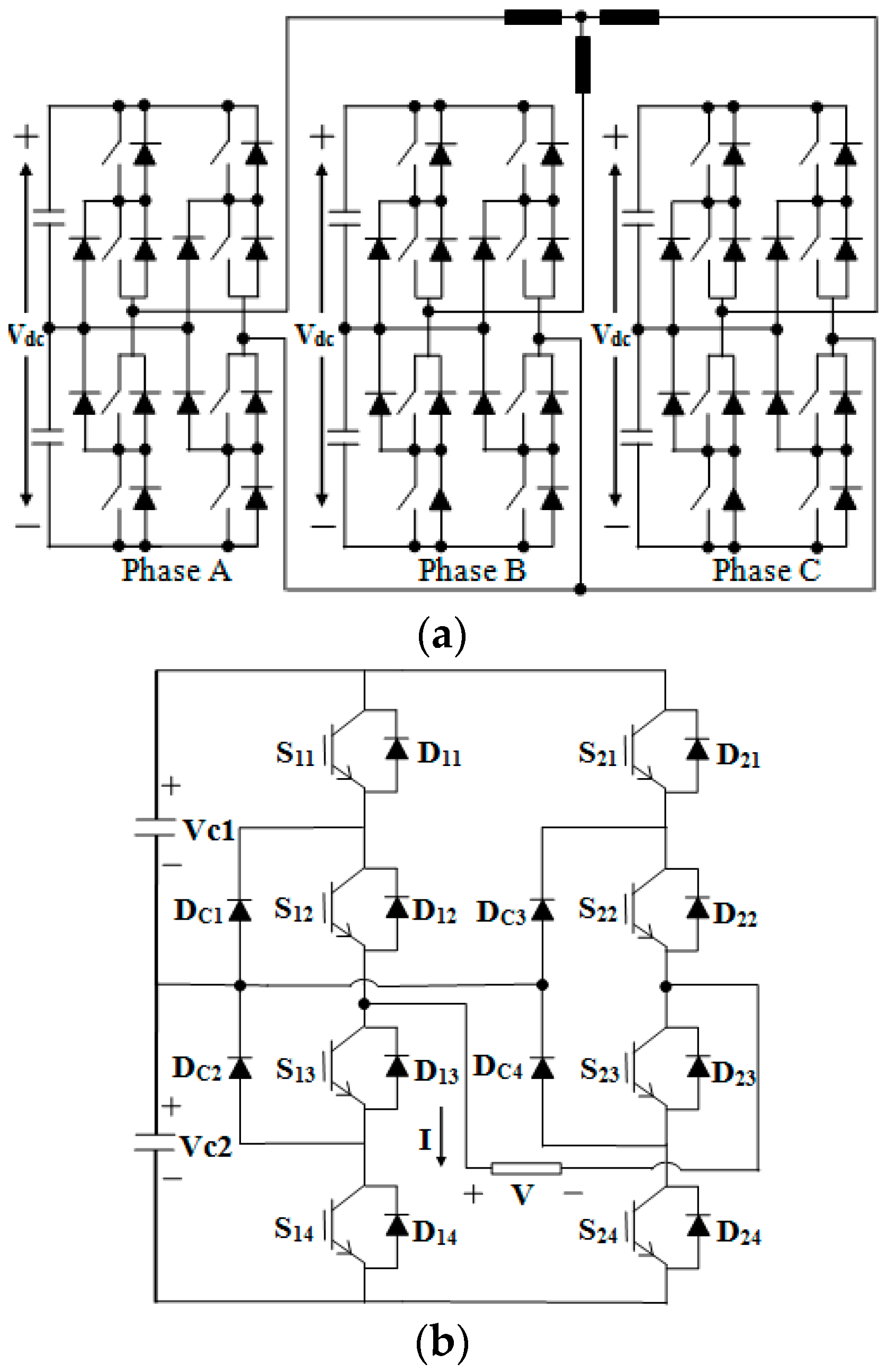
Figure 1a, each phase of a three-phase five-level NPC/H-Bridge inverter comprises a single-phase five-level NPC module fed by isolated DC power supplies.
Ensuring service continuity in many safety-critical applications is indispensable, particularly in cases where multilevel converters are used. On the other hand, the multilevel converters are comprised of numerous semiconductor components. This feature increases the possibility of fault occurrence [4]. An open-circuit fault event in a power component brings about terminal current and voltage distortion in the multilevel inverters. If this faulty condition subsists for a long time, it can lead to destructive effects [5]. In addition to the adverse impacts of the current and voltage distortion, an open-circuit fault event can also expose the DC link capacitors to breakdown. For instance, in the case of an open-circuit fault occurrence in a clamping diode of a five-level NPC/H-Bridge inverter, the neutral-point voltage would diverge from its rated value, which subjects one of the DC link capacitors to overvoltage and eventually to breakdown. This phenomenon is addressed in this paper.
Some research efforts have been carried out on fault-tolerance control in multilevel converters. The research efforts dealing with fault-tolerant operation in the inverters can be assessed based on six main criteria such as restoring rated output voltage and output current during post-fault operation, harmonic distortion of terminal voltage and current during remedial operation, ensuring service continuity in case of a fault event in any active switch, ensuring fault-tolerant operation in case of a fault occurrence in a clamping diode (in NPC converters), avoiding use of any bidirectional switch or contactor and ensuring service continuity in the case of a fault event in the anti-parallel diodes.
The research works carried out in this field of study can be classified into two main groups. The research works presented in [1,6,7,8,9,10,11] which employ redundant components fall into the first group, and the studies presented in [5,12,13,14,15,16,17,18,19,20] which propose a fault-tolerant strategy without using any redundant component are classified as the second group.
The authors in [1] propose a fault-tolerant inverter which is almost derived from the combination of an NPC and a T-Type topology. This cannot ensure service continuity in case of a fault event in a clamping diode. In [6], six contactors are utilized to carry out the reconfiguration for an NPC inverter which leads to a high response time (tens of ms). The converter presented in [7] is evolved from the combination of a three-level NPC inverter and a fourth leg with a flying capacitor structure. In the case of a fault occurrence in a clamping diode, the fault-tolerant operation is not achieved. In [8], a fault-tolerant topology for a three-level ANPC inverter is proposed. In some fault cases, the two-level switching is adopted which leads to an increase in the harmonic distortion in the terminal voltage and current. A three-level T-type inverter is presented in [9] where bidirectional switches and fuses are employed to carry out reconfiguration. The proposed structure cannot ensure the achieving of the rated terminal voltage and current during fault-tolerant operation in case of a fault event in any switch. Furthermore, the harmonic content of the terminal voltage and current is increased during fault-tolerant operation. The authors in [10] propose a two-level voltage modulation to ensure service continuity for a T-type inverter which increases the harmonic content the terminal voltage and current. The research work conducted in [11] presents a new single-phase fault-tolerant structure. The proposed strategy cannot restore the rated voltage and current for all fault cases during fault-tolerant operation. It should be mentioned that none of the research works falling into the first group ensure service continuity in case of a fault in the anti-parallel diodes. The research works addressed hereafter pertain to the second group which do not employ any redundant switch.
In [5,18,19], in case of component breakdown located in the vertical legs, the modulation index cannot be greater than 0.5. In case of a breakdown in a neutral-point leg, the total harmonic distortion of the output voltage is increased. The authors in [12] present an approach for fault-tolerance control of the NPC and T-Type converters. In the case of breakdown of an internal semiconductor, the converter has a two-level operation which increases the total harmonic distortion of the output current. Furthermore, fault-tolerant control for an open-clamping diode fault is not studied. In [13], two-level voltage modulation is applied to achieve fault-tolerant operation. Thus, the total harmonic distortion of the output current is increased. The breakdown of a power switch is not investigated in this work. The fault-tolerant NPC inverter presented in [14] is not able to acquire the rated terminal voltage during fault-tolerant operation. In [15], the fault-tolerant operation in the case of a fault event in the clamping diode is indirectly addressed. To this end, a fuse is connected in series with each clamping diode. Hence, in case of a fault event in a switch, one of the fuses blows, which translates into an open-circuit fault event in the clamping diode connected in series with the blown fuse. The two-level voltage modulation is adopted during the fault-tolerant operation, which increases the total harmonic distortion of the output voltage. The authors in [16] have presented a fault-tolerant strategy which is similar to that presented in [12], but it cannot achieve fault-tolerant operation in the case of breakdown in an internal power switch and a clamping diode. In [17], a modified carrier-based pulse-width modulation method is applied to a three-level ANPC inverter. This strategy cannot restore the rated terminal voltage during the fault-tolerant operation. It should be mentioned that none of the research works classified into the second group can ensure fault-tolerant operation in the case of breakdown in the anti-parallel diodes. In [21], the authors propose a fault-tolerant hybrid A-NPC converter. In this work, the total harmonic distortion of the output voltage increases in some fault cases. In [22], an asymmetric fault-tolerant multilevel inverter has been proposed. The proposed structure is not able to restore nominal voltage and nominal total harmonic distortion in all fault cases. The authors of [23] present a fault-tolerant NPC inverter employed as a motor drive. The proposed approach cannot ensure nominal operation following a breakdown.
This research work presents a comprehensive fault-tolerance structure as well as the associated strategy with the aim of providing the rated output voltage and the output of a three-phase five-level NPC inverter during fault-tolerance control. The proposed strategy can also ensure fault-tolerant operation in case of fault-occurrence in a clamping diode. Total harmonic distortion of the output voltage and current is not increased during fault-tolerance control. Moreover, the power losses due to the bidirectional switches during post fault operation are avoided. Furthermore, thanks to the proposed topology, the fault-tolerant operation is ensured in the case of a fault event in the anti-parallel diodes, something which has never been seen in the cited research works. This fault-tolerant topology and remedial control is designed with the objective of satisfying the six previously mentioned criteria together. To facilitate the comparison of this research work with the previously conducted studies, Table 1 is provided in which the design criteria satisfied by each research work are indicated.
As demonstrated in Table 1, none of the research works can satisfy at least two of the six criteria.
The addition of four switches complicates the structure of the converter. However, this new structure offers the following advantages together:
  • The rated voltage and rated current are restored during fault-tolerant operation in case of a fault event either in a power switch or in a clamping diode. In other words, there is no limit for the modulation index during fault-tolerant operation.
  • The THD value of the terminal voltage and current obtained during healthy operation is preserved (the harmonic content of the terminal voltage and current is not increased during fault-tolerant operation).
  • Fault-tolerant operation of the inverter is ensured in case of a fault event in a clamping diode.
  • Bidirectional switches are not employed, which allows for the fast triggering of the fault-tolerant operation.
  • The proposed strategy ensures service continuity in case of a fault event in the anti-parallel diodes.
According to all the research works conducted in this field, there are two major solutions offered in order to ensure service continuity in a power electronic converter.. The first one is realizing fault-tolerant operation without using redundant components. In this case, the remedial control is inevitably applied using the redundant states. It should be noted that the first solution cannot ensure the restoring of the terminal voltage and current (in terms of harmonic content and amplitude) for all the fault cases. The second solution is a reconfiguration (using the redundant components) of the converter and an adaption of the switching states applied to the switches. Applying the second solution to obtain rated terminal voltage and current for all fault cases cannot be cost effective or even feasible. Indeed, by employing the two solutions and optimizing them, the propped structure offers the above-mentioned advantages together.
In this research work, the term self-healing means a feature that allows the proposed structure to restore its nominal operation, without any interrupt or intervention, following a fault event in a diode or switch.
The rest of this paper is organized as follows: the second section presents the designed fault-tolerant topology. In Section 3, the proposed fault-tolerant strategy in the case of a fault occurrence in a clamping diode or in a switch is explained. In Section 4, some selected simulation results are provided and discussed. In Section 5, some experimental results are presented. Finally, in Section 6, conclusions are drawn.

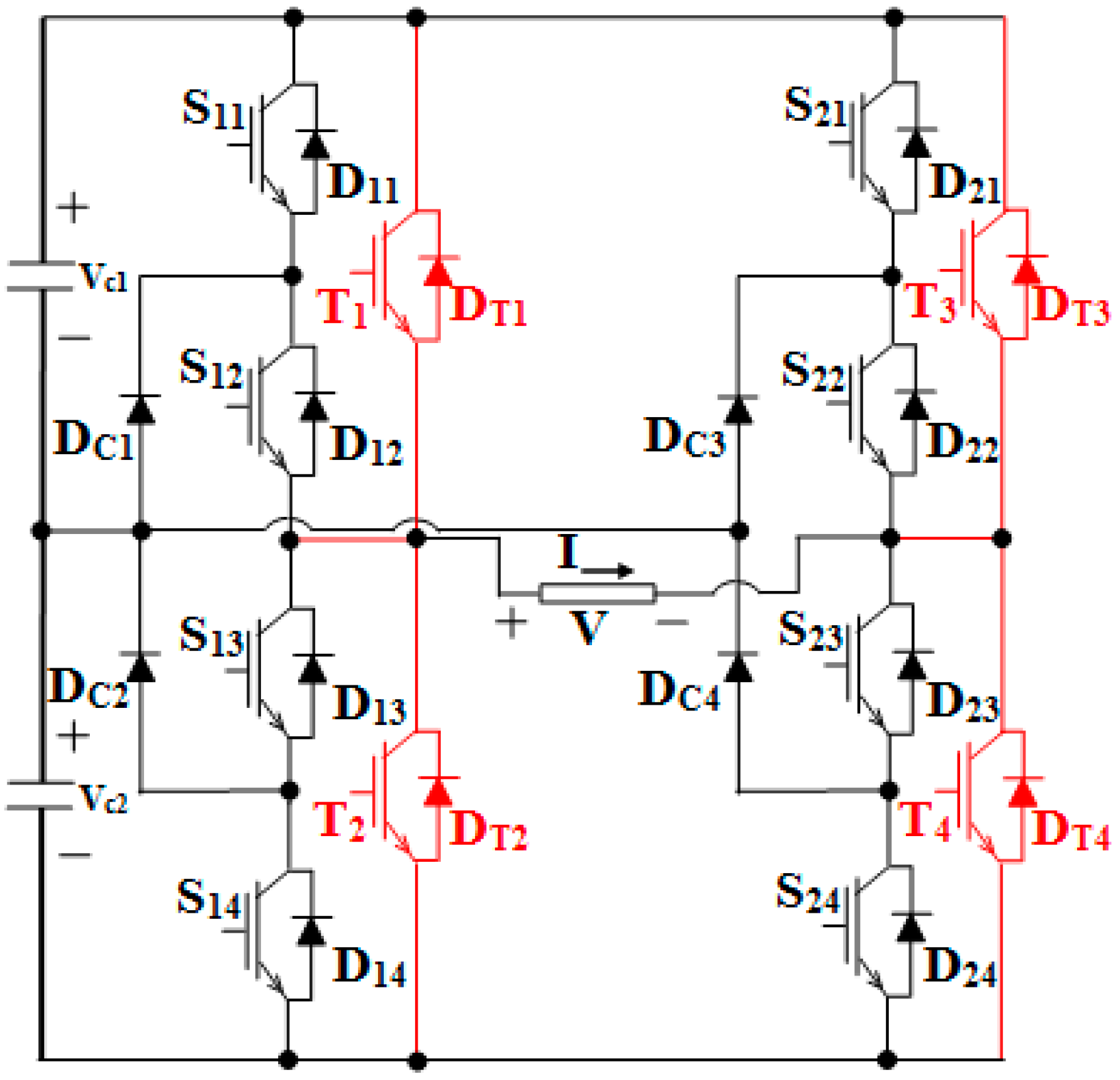
2. Fault-Tolerant Topology

As illustrated in Figure 1a, each phase of a three-phase five-level NPC inverter is constituted of a single-phase five-level NPC module. The scheme of the studied single-phase five-level NPC inverter is depicted in Figure 1b. As mentioned in the previous section, there is no bidirectional switch between the phases, as well as in each single-phase NPC module. Hence, the fault-tolerant operation in each phase is ensured independently of those in the other two phases. In this regard, acquiring fault-tolerant operation is investigated in this paper for a single-phase five-level NPC module. The proposed fault-tolerant topology is represented in Figure 2. As can be seen, the redundant components (T1, DT1), (T2, DT2), (T3, DT3), and (T4, DT4), indicated by the red color, are permanently inserted in the circuit. In healthy operation, any command signal is not applied to these redundant switches. The components conducting in each switching state and the corresponding switching pattern are tabulated in Table 2 and Table 3, respectively. The rows highlighted in gray in Table 2 and Table 3 (from switching state 10 to 17) are exclusively used during open-switch fault-tolerant operation. It should be noted that redundant anti-parallel diodes (DT1, DT2, DT3 and DT4), even in healthy operation, contribute to form the current path. Not only does this matter not cause any problem, but it also provides redundancy for the main anti-parallel diodes (D11, D12, D13, D14, D21, D22, D23 and D24), because according to Table 2, a redundant anti-parallel diode always conducts in parallel with two main anti-parallel diodes located in the same half-leg. It should be noted that in the case of a fault event in a main anti-parallel diode, the fault-tolerant operation is immediately realized without fault diagnosis because in this case, the current flows through the corresponding redundant anti-parallel diode.
In order to realize fault-tolerant operation in the case of a fault event in a clamping diode, any redundant switch is not required. In this case, the remedial operation is exclusively carried out by modifying the switching commands. In order to acquire open-switch fault-tolerant operation, using the redundant switches is indispensable.

3. Principle of the Proposed Fault-Tolerant Strategy

3.1. Open Circuit Fault in Clamping Diode

According to Table 2, in switching states 3, 5 and 7, the terminal current flows through DC1 (positive current) or DC2 (negative current). Thus, in the case of an open-circuit fault event in DC1 or DC2, the expected terminal voltages corresponding to switching states 3, 5 and 7 are not achievable. In this regard, as represented in Table 4, switching state 3 is replaced by switching state 2 to attain the same terminal voltage +Vdc/2. As shown in Table 2, in switching state 2 (either for positive current or negative current), the terminal current does not pass through DC1 or DC2. Hence, the terminal voltage can attain +Vdc/2, as desired. Switching state 5 can be substituted with switching state 4 or 6 in which no clamping diode conducts the terminal current. It should be noted that the switching states 4 and 6 have the same impact on the neutral point and DC link capacitors’ voltages because in switching state 4 or switching state 6 (see Table 2), no current is injected to the neutral point. Therefore, 0 V is made at the terminal either by substituting switching state 4 or switching state 6. In order to obtain −Vdc/2 at the terminal, switching state 7 is replaced by switching state 8. As can be seen in Table 2, in switching state 8, the terminal current does not pass through clamping diodes DC1 or DC2. Likewise, in Table 4 the rows corresponding to the faulty clamping diodes DC3 or DC4 are presented. In the case of a fault occurrence in DC3 or DC4, switching states 2, 5 and 8 have to be replaced by switching states 3, 4 or 6, and 7, respectively.

3.2. Open Switch Fault-Tolerant Case

As the fault-tolerant topology is symmetric, to avoid any verbosity, the open-switch fault-tolerant approaches used for S11 and S12 are elaborated in this section. As mentioned previously, to realize fault-tolerant operation in case of a fault event in a switch, using a redundant component is compulsory. In accordance with Table 2, when switching states 1, 2 and 4 (while 1 > 0) are applied during healthy operation, the terminal current flows through S11. Thus, when S11 encounters an open-circuit fault, the voltage levels corresponding to the mentioned switching states are not achievable at the terminal. For instance, the voltage level +Vdc (while 1 > 0) is achievable by applying switching state 1 in which S11, S12, S23 and S24 form the current path (while 1 > 0). Thus, in case of a fault event in S11, the voltage level +Vdc is no longer achievable at the terminal. In this respect, as represented in Table 4, switching state 1 is replaced by switching state 10 in which T1, S23 and S24 (while 1 > 0) constitute the current path. Thus, the voltage level +Vdc is made at the terminal. In addition, as can be seen in Table 2, in case of a fault occurrence in S11, switching state 2 (while 1 > 0) is not feasible. Hence, according to Table 4, switching state 2 is substituted with switching state 11 to achieve +Vdc/2 at the terminal.
In accordance with Table 2, during healthy operation, switch S12 forms the current path when switching states 1, 2, 3, 5 and 7 (while 1 > 0) are applied. Therefore, in case of a fault event in S12, the voltage levels corresponding to the mentioned switching states are not attained at the terminal. In this case, as can be observed in Table 4, infeasible switching states 1, 2, 3, 4, 5 and 7 are substituted with switching states 10, 11, 11, 6, 6 and 8, respectively. As can be observed in Table 2, in substituted switching states 6, 8, 10 and 11 (while 1 > 0), the terminal current does not pass through S12. Similarly to the previous subsection, it should be noted that the three switching states 4, 5 and 6 which result in 0 V at the terminal have the same impact on the DC-link capacitors, because in these switching states no current is injected to the neutral point. Thus, according to the faulty case, these three switching states can be used interchangeably. Likewise, the infeasible switching states and the corresponding substituted switching states for all switches are summarized in Table 4.
According to all research works conducted in this field, in order to ensure service continuity of a power electronic converter, two major solutions are offered. The first one is realizing fault-tolerant operation without using redundant components. In this case, the remedial control is inevitably applied using the redundant states, but it cannot restore the rated voltage and current as well as the desired harmonic content for all fault cases. The second solution is reconfiguration (using the redundant components) of the converter and adapting the switching states applied to the switches. Using this solution to obtain rated voltage and current as well as desired harmonic content cannot be cost effective or even feasible. Indeed, the innovation of this research is that it employs the two solutions and optimizes them to satisfy all the criteria mentioned in Section 1 and summarized in Table 1.

4. Simulation Results

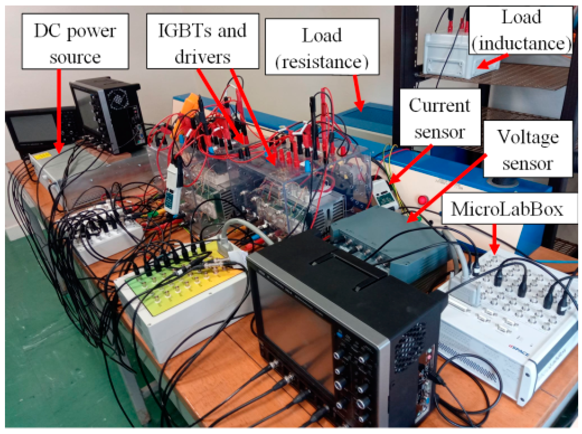
The simulation results are represented in the two following subsections. In the first one, the simulation results concerning the open-clamping diode fault-tolerant operation are provided and discussed. In the second one, the simulation results regarding the fault-tolerant strategy in case of a fault event in a power switch are presented. Since the topology of the converter is symmetric, clamping diode DC4 and switches S11 and S12 are chosen as the faulty components. The load resistance, the load inductance, the switching frequency, the fundamental frequency, the DC link capacitors, the DC link voltage and the modulation index are set at 27.7 Ω, 9 mH, 1 kHz, 50 Hz, 2.2 mF, 50 V and 0.8, respectively. These values are set based on the available hardware in our laboratory.
Matlab/Simulink environment was used to carry out the simulations. The fixed step method (step of 1 µs) has been set.

4.1. Remedial Operation in the Case of a Fault Event in a Clamping Diode

The proposed open-clamping diode fault-tolerant strategy does not require any additional or redundant component. Solely by modifying the infeasible switching states applied in healthy operation (see Table 4), service continuity is ensured. 
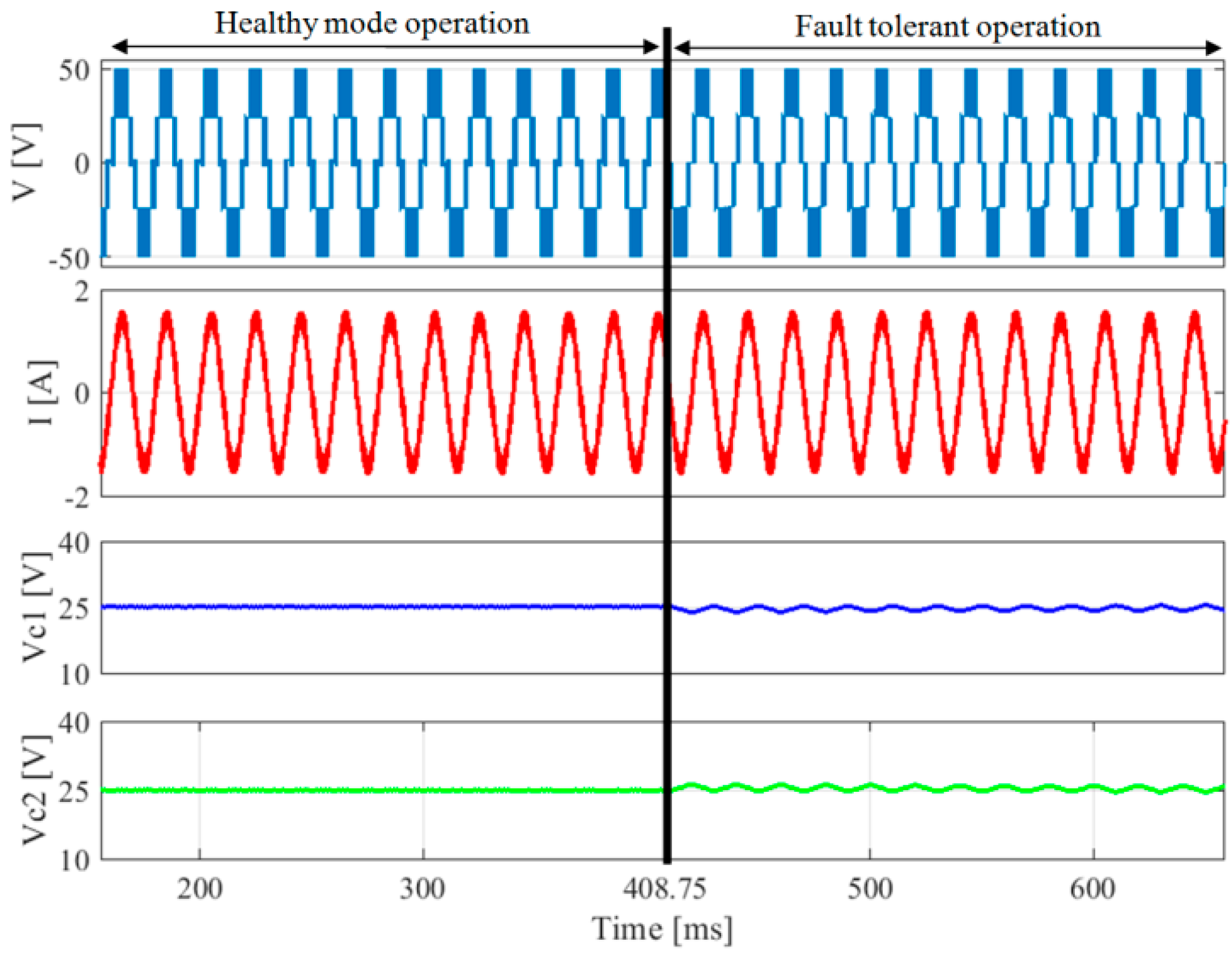
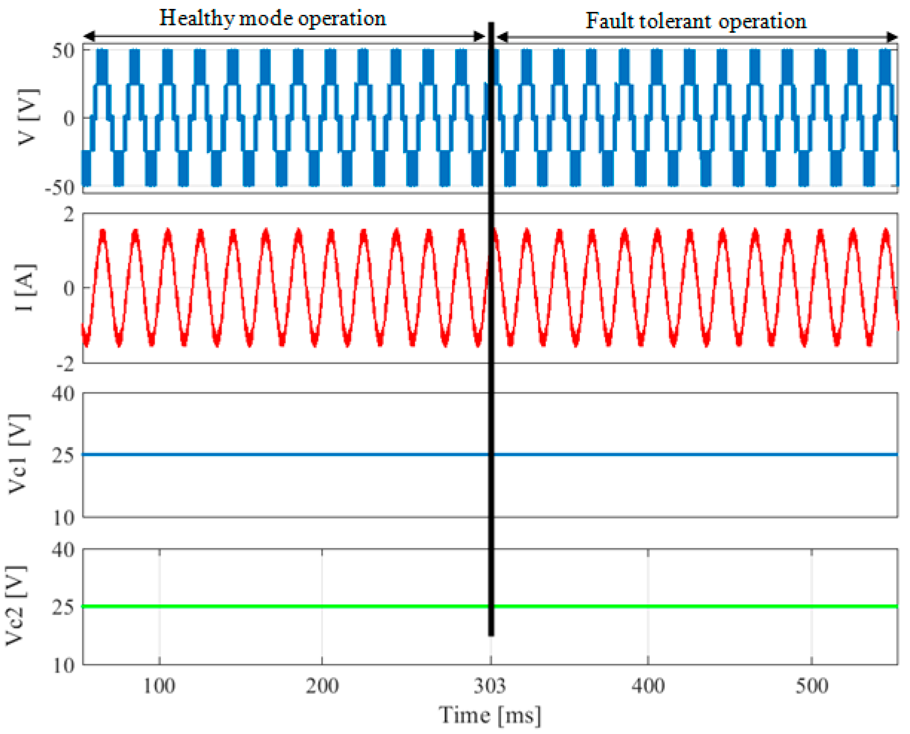
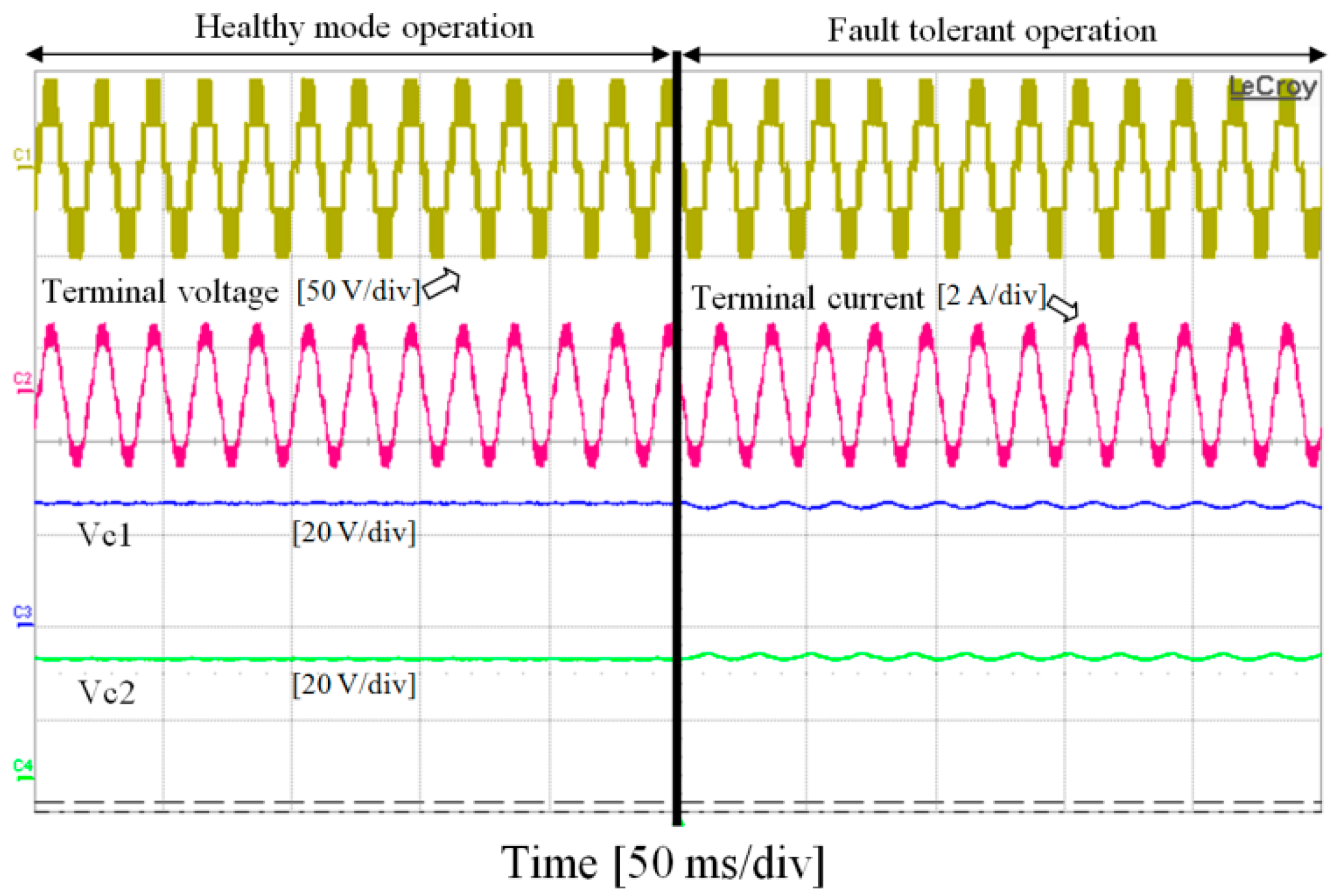
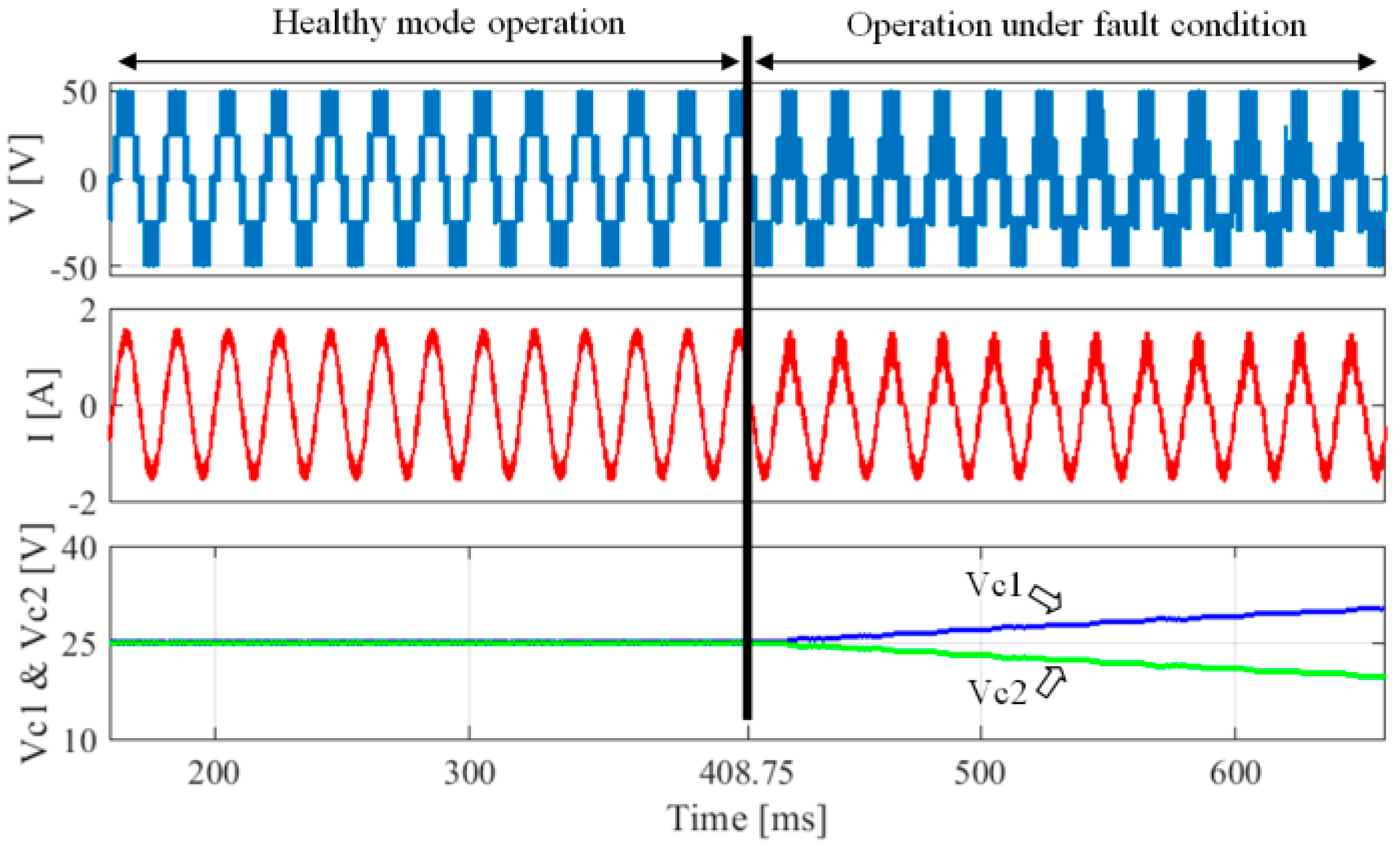
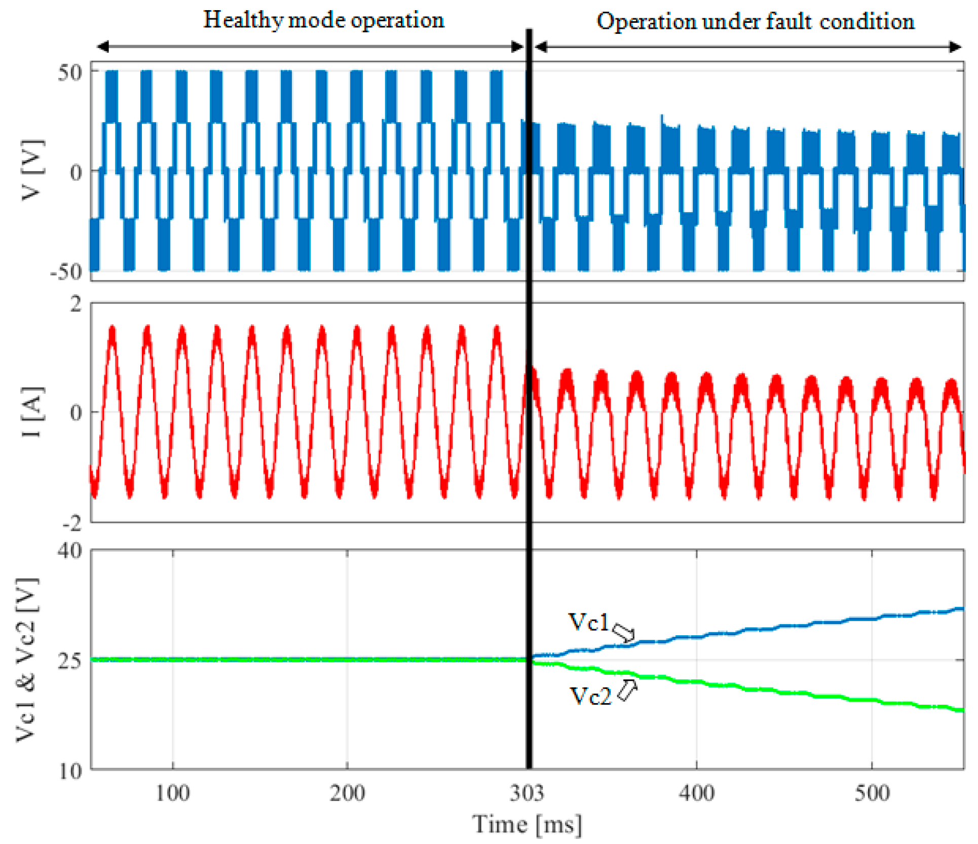
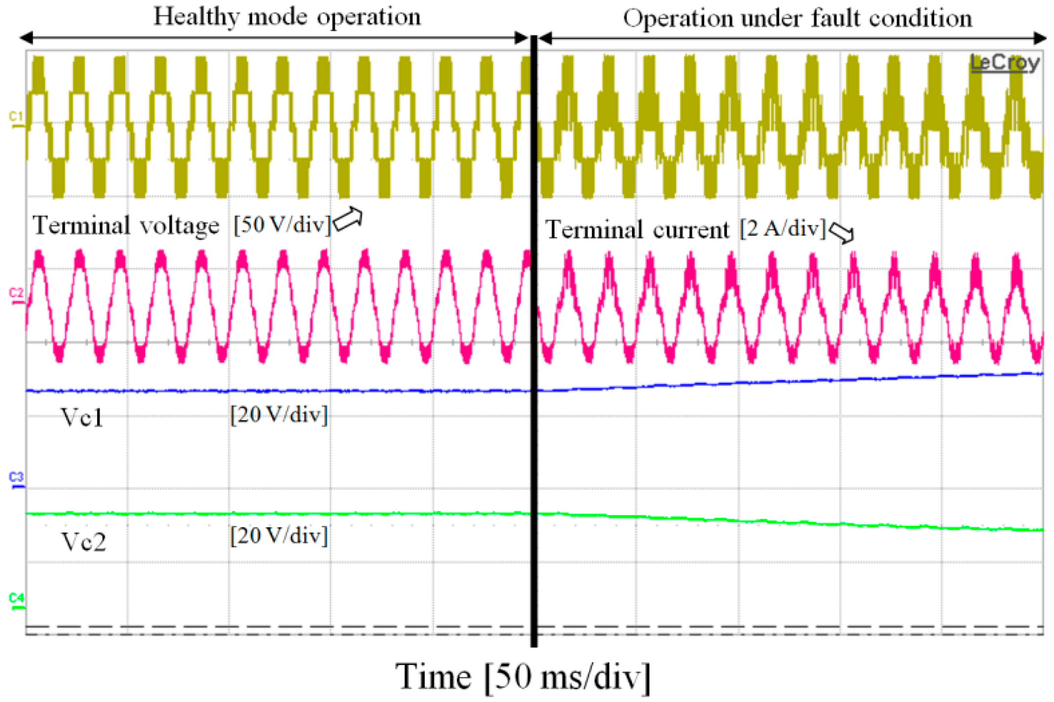
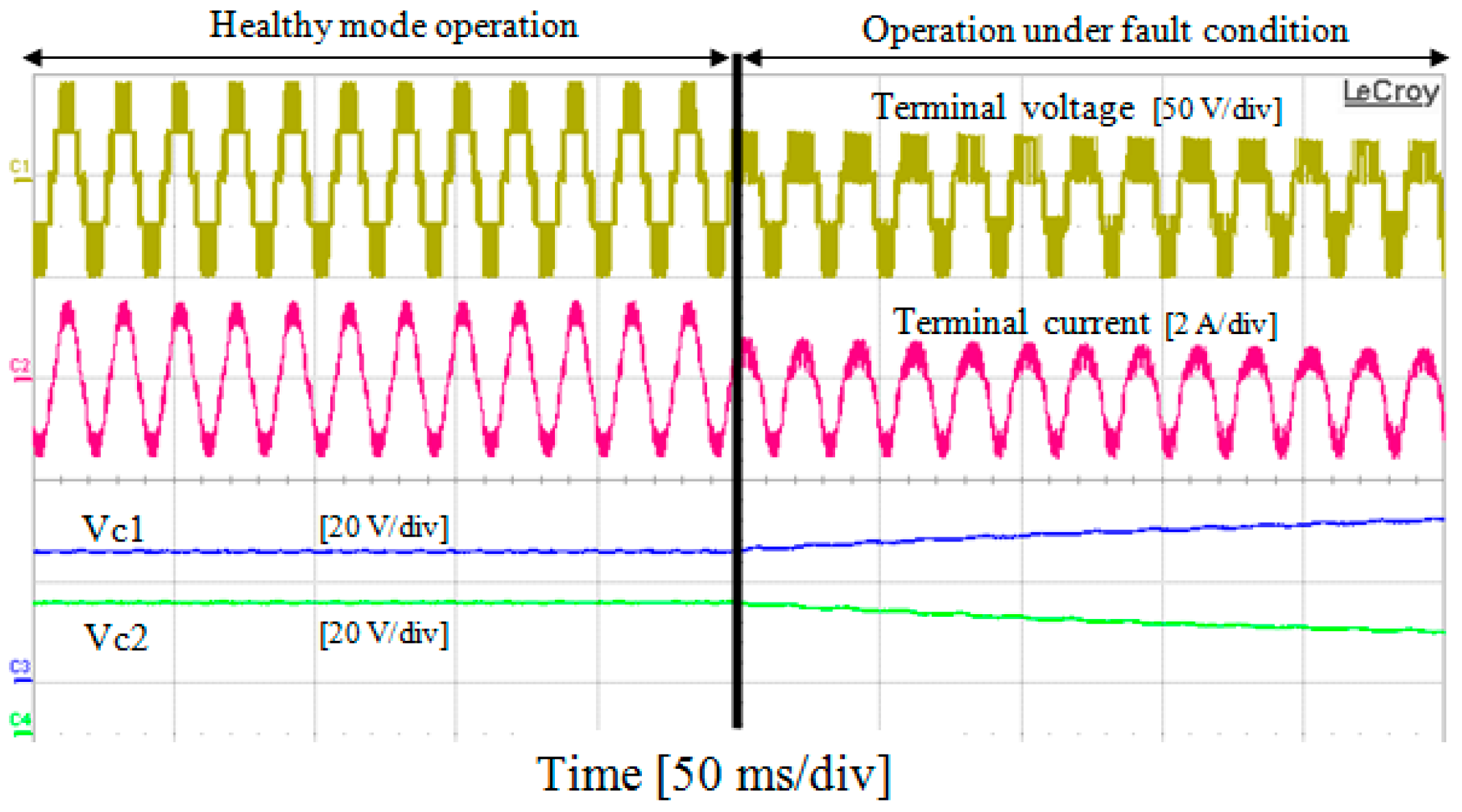
Figure 3 represents the inverter operation in the case of an open-circuit fault occurrence in DC4 without applying fault-tolerant strategy. As can be seen, once the fault occurs, the two DC link capacitors’ voltages start to diverge from their rated values in such a way that one of them attains entire DC link voltage and the other one would be discharged completely. Thus, one of the capacitors would be exposed to overvoltage. Furthermore, after the fault event, the terminal voltage and current are deteriorated in terms of distortion. The outcomes of the applied fault-tolerant strategy (in case of a fault event in DC4) are illustrated in Figure 4 and Figure 5. As shown in Figure 4, by applying the fault-tolerant strategy, the terminal and current voltage obtained during fault-tolerant operation are identical to those obtained during healthy operation.
Moreover, despite low frequency oscillation with negligible ripple amplitude (around 1.5 V peak to peak) in the DC link capacitors’ voltages, the neutral point voltage is stabilized. In 
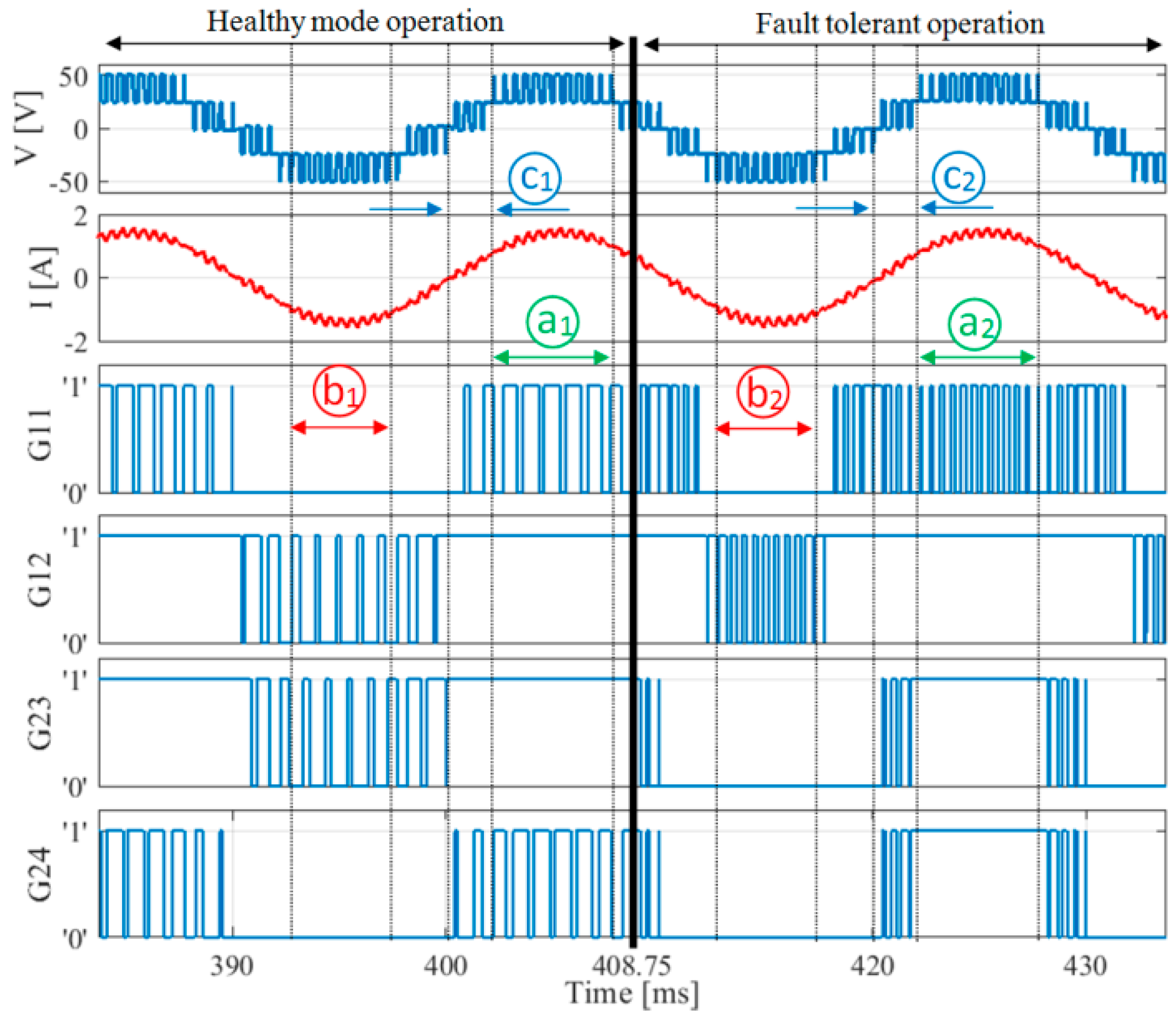
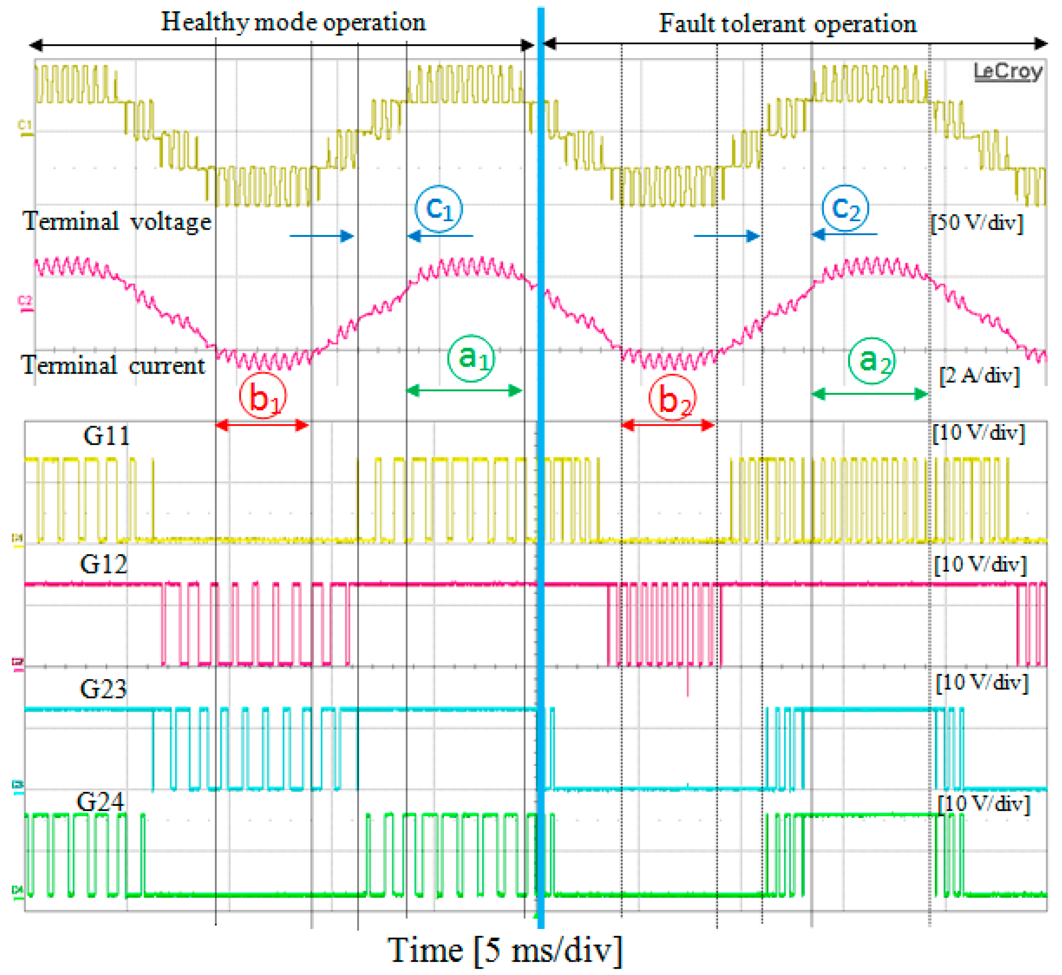
Figure 5, by comparing the healthy operation with the fault-tolerant operation of the inverter (in case of a fault event in DC4), the modifications of the switching states are represented. In this regard, the switching states corresponding to the same voltage levels (healthy operation and fault-tolerant operation) obtained at the terminal are compared. In Figure 5, four gate signals comprising G11 (gate signal of S11), G12 (gate signal of S12), G23 (gate signal of S23) and G24 (gate signal of S24) are selected to represent the applied switching states. Gate signals applied to S13, S14, S21 and S22 are complementary to those corresponding to S11, S12, S23, and S24, respectively (see Table 3). Thus, from the four mentioned gate signals, the corresponding switching state is determined. In interval a1, the voltage levels made at the terminal in healthy mode are +Vdc and +Vdc/2. According to the gate signals and Table 3, switching states 1, 2 and 3 are applied in this interval. In interval a2, the same terminal voltage levels are obtained compared with interval a1 but the switching state 2 is substituted by switching state 3. In fact, over entire interval a2, G12, G23 and G24 are set at ‘1’ and solely G11 is toggled between ‘0’ and ‘1’ which complies with Table 4, according to the switching patterns provided in Table 3 for switching states 1, 2 and 3. In interval b1 the terminal voltage levels −Vdc and −Vdc/2 are achieved. Based on the represented gate signals in interval b1 and Table 3, switching states 7, 8 and 9 are applied in this interval. By performing a detailed comparison between the gate signals applied in interval b2 (fault-tolerant operation) with those applied in interval b1, one can deduce that switching state 8 is replaced by switching state 7 (G11, G23 and G24 are set at ‘0’ and G12 is toggled between ‘0’ and ‘1’) which conforms to the data provided in Table 4. Likewise, by comparison of interval c1 with interval c2, it is deduced that during fault-tolerant operation, switching states 2 and 5 are substituted by switching states 3 and 4, respectively.

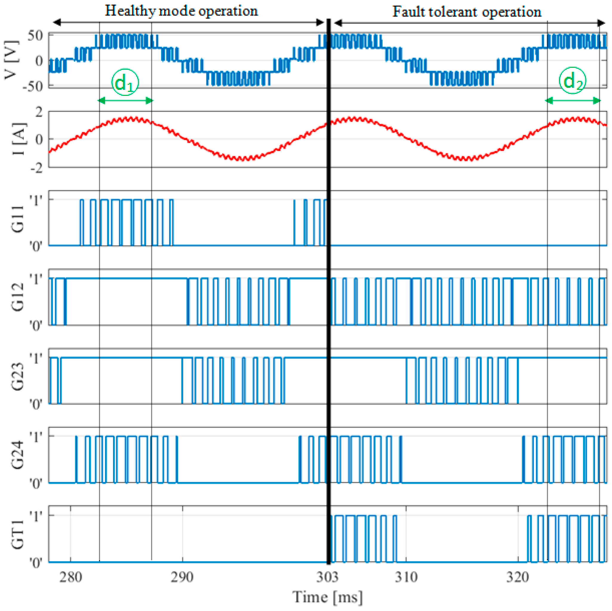
4.2. Fault-Tolerant Operation in Case of Fault Event in a Switch

As can be seen in Figure 6, subsequently to fault generation in S11, the voltage level +Vdc is no longer achievable. Furthermore, the DC link capacitors’ voltages diverge from their rated value. As can be observed in Figure 7, by applying fault-tolerant strategy subsequently to the fault occurrence, the rated current as well as the rated voltage are acquired, which are identical to those in healthy operation.
Furthermore, the DC link capacitors’ voltages are stabilized at their rated value during fault-tolerant operation. Figure 8 represents the applied gate signals during healthy and fault-tolerant operation, allowing us to observe the modification of switching states due to the applied fault-tolerant strategy. During interval d1, command signals G12, G23 and GT1 (gate signal of T1) are set at ‘1’, ‘1’ and ‘0’, respectively, and gate signals G11 and G24 toggle between ‘0’ and ‘1’. Thus, in accordance with the data tabulated in Table 3, it is deduced that switching states 1, 2 and 3 are applied during interval d1. To observe the modification of the switching states due to the fault-tolerant strategy, interval d2, during which the terminal voltage and current are identical to those in interval d1, is chosen. According to Figure 8, during interval d2, gate signals G11 and G23 are set at ‘0’ and gate signals G12, G24 and GT1 toggle between ‘0’ and ‘1’. Thus, by referring to Table 3, it is deduced that the switching states 3, 10 and 11 are applied during this interval. Hence, by comparing the switching states applied during interval d1 (healthy operation) with those applied during interval d2 (fault-tolerant operation), it is concluded that switching states 1 and 2 are replaced by switching states 10 and 11, which complies with the data provided in Table 4 (the row corresponding to faulty switch S11).
In this research work, the classical pulse-width modulation (PWM) method has been adopted. However, it should be noted that the proposed strategy is valid for all types of modulation strategies.
As discussed in the paper, the proposed structure associated with the fault-tolerant approach is able to restore nominal operation during fault-tolerant operation in case of a fault event in a switch or diode. Since nominal operation is perfectly restored during fault-tolerant operation, this approach cannot be assessed numerically or quantitatively.
During healthy operation, the total harmonic distortion (THD) of the terminal current is 8.5%. In case of a fault event in DC4, without applying the remedial control, the THD of the terminal current reaches 21%. By applying the remedial control, the THD value of the terminal current attains 8.5%.
In case of a fault occurrence in S11, without applying the remedial control and reconfiguration, the THD of the terminal current reaches 25%. During fault-tolerant operation, the THD value of the terminal current reaches the level obtained during healthy operation.

5. Experimental Results

For the implementation of the proposed fault-tolerant strategy, a MicroLabBox (one of the dSPACE platforms) including a processor and an FPGA chip (Xilinx® Kintex®-7 XC7K325T) is employed. Since the modifications of the switching states during post-fault operation should be performed as quickly as possible, the proposed fault-tolerant strategy is realized by the FPGA-based module of the MicroLabBox in order to reduce the transition time between healthy and fault-tolerant operation. The inverter is constituted of the IGBTs SKM50GB123D of SEMIKRON, commanded by SKHI22A drivers. The clock frequency of the FPGA module is set at 100 MHz. The experimental setup is represented in Figure 9. For the experimental setup, all parameters are the same as those reported in the simulation section. In order to generate the open-circuit fault in a clamping diode, an auxilliary IGBT is placed in series with the concerned clamping diode. In the healthy mode operation, the gate signal of the IGBT connected in series with the relevant clamping diode is established constantly. In order to generate the open-circuit fault in the clamping diode, the gate signal of the auxilliary IGBT is removed. For generating an open-circuit fault in an IGBT, the gate signal corresponding to the concerned IGBT is removed. Similarly to the simulation section, clamping diode DC4 and switch S11 are considered as the faulty components. Since the results presented in Figure 10, Figure 11, Figure 12, Figure 13 and Figure 14 are almost identical to those presented in Figure 3, Figure 4, Figure 5, Figure 6, Figure 7 and Figure 8, respectively, any repetitive explanation is avoided in this section. A comprehensive analysis and explanations are given and discussed in the previous subsection.
It should be noted that the transition time between healthy operation and fault-tolerant control arises from the time required for fault diagnosis. Since in this research work fault diagnosis is accomplished within some tens of µs, the mentioned transition time is not visible in Figure 11, Figure 12 and Figure 14. The authors have comprehensively presented the fault diagnosis method in [20]. It should be noted that the applied fault-tolerant control is independent of the fault diagnosis strategy and is compatible to any fault diagnosis strategy.

6. Conclusions

In this paper, a fault-tolerant five-level NPC inverter with the aim of achieving the rated terminal voltage and current during fault-tolerant operation has been presented. The proposed fault-tolerant strategy not only ensures fault-tolerant operation in case of a fault event in a switch but also guarantees fault-tolerant operation in case of a fault occurrence in a clamping diode. As has been presented in this paper, fault occurrence in a clamping diode can expose one of the DC link capacitors to over voltage and breakdown. In this regard, presenting a remedial operation in case of a fault event in a clamping diode is of considerable importance, and is rarely seen in the literature. In order to realize fault-tolerant operation in the case of a fault event in a clamping diode, solely the switching states are modified. Compared to healthy operation, the harmonic content of the terminal voltage and current is not increased during fault-tolerant operation. Since no bidirectional switch neither in a single-phase module nor between the phases is employed, a fast transition between healthy operation and fault-tolerant operation is achieved and the power losses due to the bidirectional switches during post-fault operation are avoided. Furthermore, thanks to the proposed fault-tolerant topology, fault-tolerant operation of the inverter is ensured when any anti-parallel diode encounters an open-circuit fault which is overlooked in the literature. Based on the research works conducted in this field, fault-tolerant strategy is realized by using the additional components or modifying the switching pattern, which does not include a remarkable mathematical background. In this research work, by optimizing the two mentioned solutions, an efficient fault-tolerant strategy is proposed whose implementation does not require any complicated calculation. This feature can be considered a significant advantage because it facilitates implantation, which leads to an increase in the time performance of the proposed approach.

Author Contributions

Investigation: S.A., P.P. and S.S.; methodology: S.A., P.P. and S.S.; supervision: P.P., S.S. and D.A.K.; writing—original draft: S.A.; writing—review & editing: P.P., D.A.K. and S.S. All authors have read and agreed to the published version of the manuscript.

Funding

This research work is the result of a collaboration between the University of Lorraine (France) and the Iran University of Science and Technology (IUST) started in October 2018. It has been partially financially supported by the Scientific and Technologique Cooperation Service of the French Embassy in Tehran that we would like to thank.

Institutional Review Board Statement

Not applicable.

Informed Consent Statement

Not applicable.

Data Availability Statement

Not applicable.

Conflicts of Interest

The authors declare no conflict of interest.

References

  1. Gautam, S.P.; Kumar, L.; Gupta, S.; Agrawal, N. A single-phase five-level inverter topology with switch fault-tolerance capabilities. IEEE Trans. Ind. Electron. 2017, 64, 2004–2014. [Google Scholar] [CrossRef]
  2. Rodriguez, J.; Lai, S.; Peng, F.Z. Multilevel inverters: A survey of topologies, controls, and applications. IEEE Trans. Ind. Electron. 2002, 49, 724–738. [Google Scholar] [CrossRef] [Green Version]
  3. Wu, B. High-Power Converters AC Drives; Wiley: Hoboken, NJ, USA, 2006. [Google Scholar]
  4. Ahmadi, S.; Poure, P.; Khaburi, D.A.; Saadate, S. A Remedial Control for Short-Circuit Fault in NPC/H-Bridge Inverters without Redundant Component. Electronics 2021, 10, 2411. [Google Scholar] [CrossRef]
  5. Choi, U.-M.; Blaabjerg, F.; Lee, K.-B. Reliability improvement of a T-type three-level inverter with fault-tolerant control strategy. IEEE Trans. Power Electron. 2014, 30, 2660–2673. [Google Scholar] [CrossRef]
  6. Ceballos, S.; Pou, J.; Zaragoza, J.; Robles, E.; Villate, J.L.; Martín, J.L. Fault-tolerant neutral-point-clamped converter solutions based on including a fourth resonant leg. IEEE Trans. Ind. Electron. 2011, 58, 2293–2303. [Google Scholar] [CrossRef]
  7. Ceballos, S.; Pou, J.; Robles, E.; Gabiola, I.; Zaragoza, J.; Villate, J.L.; Boroyevich, D. Three-level converter topologies with switch breakdown fault-tolerance capability. IEEE Trans. Ind. Electron. 2008, 55, 982–995. [Google Scholar] [CrossRef]
  8. Katebi, R.; He, J.; Weise, N. An advanced three-level active neutral-point-clamped converter with improved fault-tolerant capabilities. IEEE Trans. Power Electron. 2017, 33, 6897–6909. [Google Scholar] [CrossRef] [Green Version]
  9. Xu, S.; Zhang, J.; Hang, J. Investigation of a fault-tolerant three-level T-type inverter system. IEEE Trans. Ind. Appl. 2017, 53, 4613–4623. [Google Scholar] [CrossRef]
  10. He, J.; Katebi, R.; Weise, N.; Demerdash, N.A.O.; Wei, L. A fault-tolerant T-type multilevel inverter topology with increased overload capability and soft-switching characteristics. IEEE Trans. Ind. Appl. 2017, 53, 2826–2839. [Google Scholar] [CrossRef]
  11. Choupan, R.; Golshannavaz, S.; Nazarpour, D.; Barmala, M. A new structure for multilevel inverters with fault tolerant capability against open circuit faults. Electr. Power Syst. Res. 2018, 168, 105–116. [Google Scholar] [CrossRef]
  12. Lee, J.S.; Lee, K.-B. Open-switch fault tolerance control for a three-level NPC/T-type rectifier in wind turbine systems. IEEE Trans. Ind. Electron. 2015, 62, 1012–1021. [Google Scholar] [CrossRef]
  13. Choi, U.-M.; Lee, J.-S.; Blaabjerg, F.; Lee, K.-B. Open-circuit fault diagnosis and fault-tolerant control for a grid-connected NPC inverter. IEEE Trans. Power Electron. 2016, 31, 7234–7247. [Google Scholar] [CrossRef]
  14. Li, S.; Xu, L. Strategies of fault tolerant operation for three-level PWM inverters. IEEE Trans. Power Electron. 2006, 21, 933–940. [Google Scholar] [CrossRef]
  15. Ceballos, S.; Pou, J.; Robles, E.; Zaragoza, J.; Martín, J.L. Performance evaluation of fault-tolerant neutral-point-clamped converters. IEEE Trans. Ind. Electron. 2010, 57, 2709–2718. [Google Scholar] [CrossRef]
  16. Lee, J.; Lee, K. Open-circuit fault-tolerant control for outer switches of three-level rectifiers in wind turbine systems. IEEE Trans. Power Electron. 2016, 31, 3806–3815. [Google Scholar] [CrossRef]
  17. Azer, P.; Ouni, S.; Narimani, M. A novel fault-tolerant technique for active neutral point clamped inverter using carrier-based PWM. IEEE Trans. Ind. Electron. 2019, 67, 1792–1803. [Google Scholar] [CrossRef]
  18. Choi, U.; Lee, K.; Blaabjerg, F. Diagnosis and tolerant strategy of an open-switch fault for T-type three-level inverter systems. IEEE Trans. Ind. Appl. 2014, 50, 495–508. [Google Scholar] [CrossRef]
  19. Lee, T.-L.; Li, B.-F.; Yang, M.-Y.; Tsai, Y.-T. A Carrier-Based PWM for Three-Level T-Type Inverter to Tolerate Open-Circuit Fault. IEEE Trans. Power Electron. 2018, 33, 8787–8796. [Google Scholar] [CrossRef]
  20. Ahmadi, S.; Poure, P.; Saadate, S.; Khaburi, D.A. A real time fault diagnosis for neutral-point-clamped inverters based on failure mode algorithm. IEEE Trans. Ind. Inform. 2021, 17, 1100. [Google Scholar] [CrossRef]
  21. Halabi, L.M.; Alsofyani, I.M.; Lee, K.-B. Open-Circuit Fault Tolerance Method for Three-Level Hybrid Active Neutral Point Clamped Converters. Electronics 2020, 9, 1535. [Google Scholar] [CrossRef]
  22. Fahad, M.; Tariq, M.; Sarwar, A.; Modabbir, M.; Zaid, M.A.; Satpathi, K.; Hussan, M.R.; Tayyab, M.; Alamri, B.; Alahmadi, A. Asymmetric Multilevel Inverter Topology and Its Fault Management Strategy for High-Reliability Applications. Energies 2021, 14, 4302. [Google Scholar] [CrossRef]
  23. Chao, K.-H.; Ke, C.-H. Fault Diagnosis and Tolerant Control of Three-Level Neutral-Point Clamped Inverters in Motor Drives. Energies 2020, 13, 6302. [Google Scholar] [CrossRef]
Figure 1. Scheme of (a) a three-phase five-level NPC/H-bridge inverter, and (b) a single-phase five-level NPC inverter.
Energies 15 04721 g001
Figure 2. Proposed fault-tolerant topology.
Energies 15 04721 g002
Figure 3. Simulation results of the inverter operation under open-circuit fault occurrence in DC4, without fault-tolerant strategy.
Energies 15 04721 g003
Figure 4. Simulation results for fault-tolerant operation of the inverter in case of fault occurrence in DC4.
Energies 15 04721 g004
Figure 5. Detailed representation of the fault-tolerant operation in case of open-circuit fault occurrence in DC4.
Energies 15 04721 g005
Figure 6. Simulation results of the inverter operation under open-circuit fault occurrence in S11, without fault-tolerant strategy.
Energies 15 04721 g006
Figure 7. Simulation results for fault-tolerant operation of the inverter in case of fault occurrence in S11.
Energies 15 04721 g007
Figure 8. Detailed representation of the fault-tolerant operation in the case of an open-circuit fault occurrence in S11.
Energies 15 04721 g008
Figure 9. Experimental setup.
Energies 15 04721 g009
Figure 10. Experimental results of the inverter operation under fault event in Dc4 without fault-tolerant control.
Energies 15 04721 g010
Figure 11. Experimental results of the inverter operation with fault-tolerant control in case of fault event in Dc4.
Energies 15 04721 g011
Figure 12. Detailed experimental results of the fault-tolerant strategy in case of fault event in Dc4.
Energies 15 04721 g012
Figure 13. Experimental results of the inverter operation under fault event in S11 without fault-tolerant control.
Energies 15 04721 g013
Figure 14. Experimental results of the inverter operation with fault-tolerant control in case of fault event in S11.
Energies 15 04721 g014
Table 1. Comparison of this research work with the state of the art.
Research WorkCriteria (Defined at the Bottom of This Table)
1st2nd3rd4th5th6th
Proposed Circuit
including redundant components[1]
[6]
[7]
[8]---
[9]---
[10]---
[11]---
without employing any redundant component[5]---
[12]
[13]
[14]
[15]
[16]
[17]---
[18]---
[19]---
1st criteria: Acquiring rated terminal current and voltage during fault-tolerant operation in case of fault event in any switch. 2nd criteria: Avoiding increasing the harmonic content of the terminal voltage and current during fault-tolerant operation in case of fault event in any switch. 3rd criteria: Ensuring fault-tolerant operation in case of fault event in any active switch. 4th criteria: Ensuring fault-tolerant operation in case of fault event in a clamping diode. 5th criteria: Avoiding using any bidirectional switch or contactor. 6th criteria: Ensuring fault-tolerant operation in case of fault event in anti-parallel diodes. ✓: The criteria is met. ✗: The criteria is not met. ---: The converter does not include any clamping diode.
Table 2. Passing components corresponding to each switching state for positive and negative output currents in healthy (States 1 to 9) and fault-tolerant operation (States 10 to 17).
StateTerminal VoltagePassing Components (I > 0)Passing Components (I < 0)
1+VdcS11, S12, S23, S24D11, D12, DT1, D23, D24, DT4
2+Vdc/2S11, S12, S23, DC4D11, D12, DT1, S22, DC3
3+Vdc/2DC1, S12, S23, S24DC2, S13, D23, D24, DT4
40S11, S12, D22, D21, DT3D11, D12, DT1, S21, S22
50DC1, S12, S23, DC4DC2, S13, S22, DC3
60D14, D13, DT2, S23, S24S13, S14, DT4, D24, D23
7−Vdc/2DC1, S12, D22, D21, DT3DC2, S13, S22, S21
8−Vdc/2D14, D13, DT2, S23, DC4S13, S14, DC3, S22
9−VdcD14, D13, DT2, D21, D22, DT3S13, S14, S22, S21
10+VdcT1, S23, S24D11, D12, DT1, D23, D24, DT4
11+Vdc/2T1, S23, DC4D11, D12, DT1, S22, DC3
12−VdcD14, D13, DT2, D21, D22, DT3T2, S21, S22
13−Vdc/2D14, D13, DT2, S23, DC4T2, S22, DC3
14−VdcD14, D13, DT2, D21, D22, DT3T3, S13, S14
15−Vdc/2DC1, S12, D22, D21, DT3DC2, S13, T3
16+VdcS11, S12, T4D11, D12, DT1, D23, D24, DT4
17+Vdc/2DC1, S12, T4DC2, S13, D23, D24, DT4
Table 3. Switching pattern corresponding to each voltage level.
State S11S12S13S14S21S22S23S24T1T2T3T4
1+Vdc110000110000
2+Vdc/2110001100000
3+Vdc/2011000110000
40110011000000
50011001100000
60001100110000
7−Vdc/2011011000000
8−Vdc/2001101100000
9−Vdc001111000000
10+Vdc000000111000
11+Vdc/2000001101000
12−Vdc000011000100
13−Vdc/2000001100100
14−Vdc001100000010
15−Vdc/2011000000010
16+Vdc110000000001
17+Vdc/2011000000001
Table 4. Modification of the switching states to realize fault-tolerant operation.
Faulty
Component
[Infeasible Switching State, Substituted Switching State]
DC1 or DC2[3, 2], [5, 4 or 6], [7, 8]
DC3 or DC4[2, 3], [5, 4 or 6], [8, 7]
S11[1, 10], [2, 11], [4, 5 or 6]
S12[1, 10], [2, 11], [3, 11], [4, 6], [5, 6], [7, 8]
S13[3, 2], [5, 4], [6, 4], [7, 13], [8, 13], [9, 12]
S14 [6, 4 or 5], [8, 13], [9, 12]
S21[4, 5 or 6], [7, 15], [9, 14]
S22[2, 3], [4, 6], [5, 6], [7, 15], [8, 15], [9, 14]
S23[1, 16], [2, 17], [3, 17], [5, 4], [6, 4], [8, 7]
S24[1, 16], [3, 17], [6, 4 or 5]
Publisher’s Note: MDPI stays neutral with regard to jurisdictional claims in published maps and institutional affiliations.

