1. Introduction
For some decades now, multilevel inverters have widely attracted industry attention. These power electronic converters present noticeable advantages compared with the two-level classical converters. These advantages include limited voltage transients, less total harmonic distortion, reduced common-mode voltage, fewer switching losses, and small sized filter elements [
1,
2]. Among the multilevel converters, neutral-point-clamped (NPC) topology has superiority over the other topologies. These converters are not comprised of a flying capacitor or isolating transformer. Because of these features, they are widely used in industry. However, in high voltage applications, dynamic and static voltage sharing problems arise across the components used in NPC topology [
3]. To cope with this constraint, NPC/H-Bridge topology is used rather than the classical NPC topology. As illustrated in
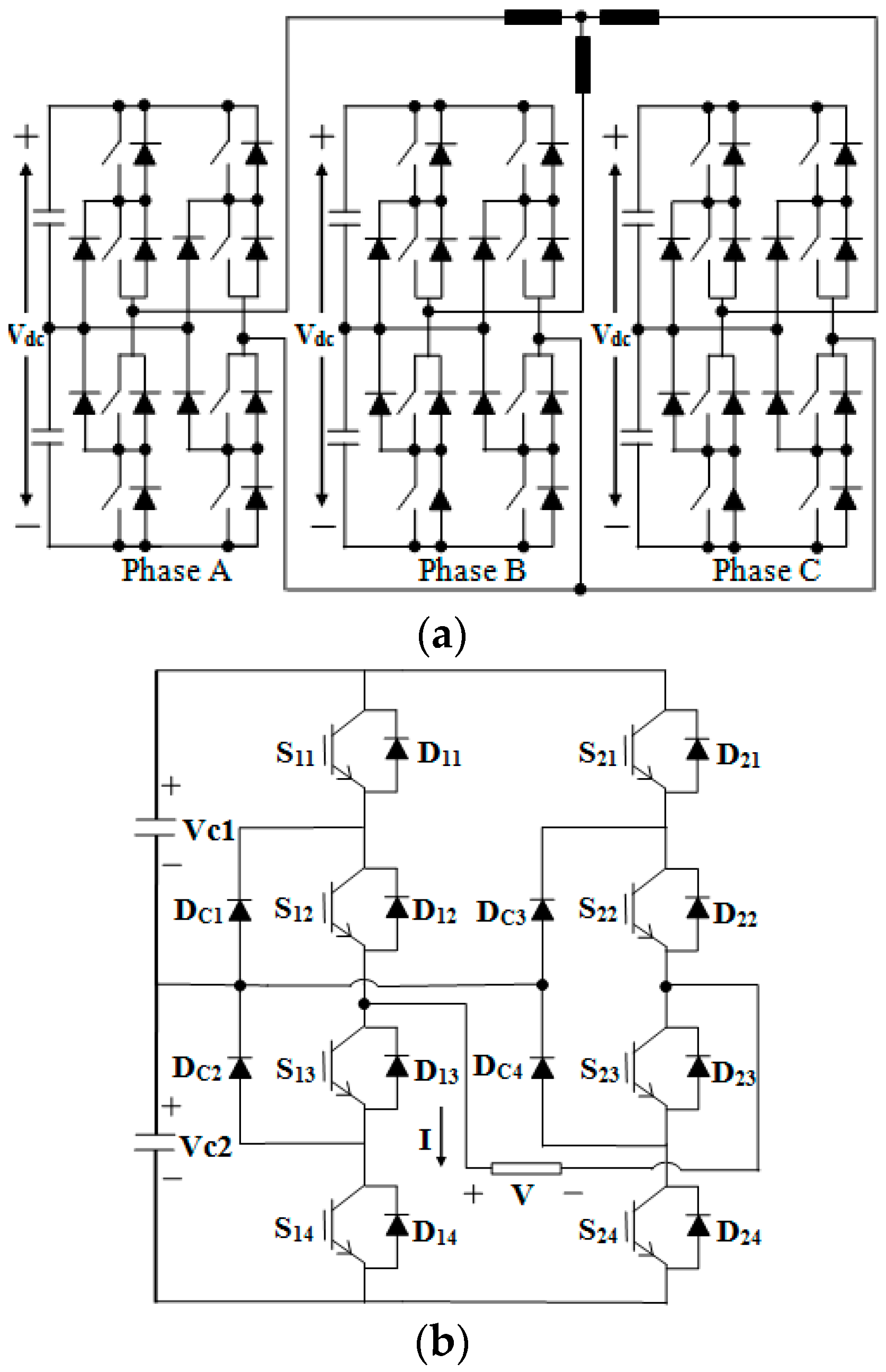
Figure 1a, each phase of a three-phase five-level NPC/H-Bridge inverter comprises a single-phase five-level NPC module fed by isolated DC power supplies.
Ensuring service continuity in many safety-critical applications is indispensable, particularly in cases where multilevel converters are used. On the other hand, the multilevel converters are comprised of numerous semiconductor components. This feature increases the possibility of fault occurrence [
4]. An open-circuit fault event in a power component brings about terminal current and voltage distortion in the multilevel inverters. If this faulty condition subsists for a long time, it can lead to destructive effects [
5]. In addition to the adverse impacts of the current and voltage distortion, an open-circuit fault event can also expose the DC link capacitors to breakdown. For instance, in the case of an open-circuit fault occurrence in a clamping diode of a five-level NPC/H-Bridge inverter, the neutral-point voltage would diverge from its rated value, which subjects one of the DC link capacitors to overvoltage and eventually to breakdown. This phenomenon is addressed in this paper.
Some research efforts have been carried out on fault-tolerance control in multilevel converters. The research efforts dealing with fault-tolerant operation in the inverters can be assessed based on six main criteria such as restoring rated output voltage and output current during post-fault operation, harmonic distortion of terminal voltage and current during remedial operation, ensuring service continuity in case of a fault event in any active switch, ensuring fault-tolerant operation in case of a fault occurrence in a clamping diode (in NPC converters), avoiding use of any bidirectional switch or contactor and ensuring service continuity in the case of a fault event in the anti-parallel diodes.
The research works carried out in this field of study can be classified into two main groups. The research works presented in [
1,
6,
7,
8,
9,
10,
11] which employ redundant components fall into the first group, and the studies presented in [
5,
12,
13,
14,
15,
16,
17,
18,
19,
20] which propose a fault-tolerant strategy without using any redundant component are classified as the second group.
The authors in [
1] propose a fault-tolerant inverter which is almost derived from the combination of an NPC and a T-Type topology. This cannot ensure service continuity in case of a fault event in a clamping diode. In [
6], six contactors are utilized to carry out the reconfiguration for an NPC inverter which leads to a high response time (tens of ms). The converter presented in [
7] is evolved from the combination of a three-level NPC inverter and a fourth leg with a flying capacitor structure. In the case of a fault occurrence in a clamping diode, the fault-tolerant operation is not achieved. In [
8], a fault-tolerant topology for a three-level ANPC inverter is proposed. In some fault cases, the two-level switching is adopted which leads to an increase in the harmonic distortion in the terminal voltage and current. A three-level T-type inverter is presented in [
9] where bidirectional switches and fuses are employed to carry out reconfiguration. The proposed structure cannot ensure the achieving of the rated terminal voltage and current during fault-tolerant operation in case of a fault event in any switch. Furthermore, the harmonic content of the terminal voltage and current is increased during fault-tolerant operation. The authors in [
10] propose a two-level voltage modulation to ensure service continuity for a T-type inverter which increases the harmonic content the terminal voltage and current. The research work conducted in [
11] presents a new single-phase fault-tolerant structure. The proposed strategy cannot restore the rated voltage and current for all fault cases during fault-tolerant operation. It should be mentioned that none of the research works falling into the first group ensure service continuity in case of a fault in the anti-parallel diodes. The research works addressed hereafter pertain to the second group which do not employ any redundant switch.
In [
5,
18,
19], in case of component breakdown located in the vertical legs, the modulation index cannot be greater than 0.5. In case of a breakdown in a neutral-point leg, the total harmonic distortion of the output voltage is increased. The authors in [
12] present an approach for fault-tolerance control of the NPC and T-Type converters. In the case of breakdown of an internal semiconductor, the converter has a two-level operation which increases the total harmonic distortion of the output current. Furthermore, fault-tolerant control for an open-clamping diode fault is not studied. In [
13], two-level voltage modulation is applied to achieve fault-tolerant operation. Thus, the total harmonic distortion of the output current is increased. The breakdown of a power switch is not investigated in this work. The fault-tolerant NPC inverter presented in [
14] is not able to acquire the rated terminal voltage during fault-tolerant operation. In [
15], the fault-tolerant operation in the case of a fault event in the clamping diode is indirectly addressed. To this end, a fuse is connected in series with each clamping diode. Hence, in case of a fault event in a switch, one of the fuses blows, which translates into an open-circuit fault event in the clamping diode connected in series with the blown fuse. The two-level voltage modulation is adopted during the fault-tolerant operation, which increases the total harmonic distortion of the output voltage. The authors in [
16] have presented a fault-tolerant strategy which is similar to that presented in [
12], but it cannot achieve fault-tolerant operation in the case of breakdown in an internal power switch and a clamping diode. In [
17], a modified carrier-based pulse-width modulation method is applied to a three-level ANPC inverter. This strategy cannot restore the rated terminal voltage during the fault-tolerant operation. It should be mentioned that none of the research works classified into the second group can ensure fault-tolerant operation in the case of breakdown in the anti-parallel diodes. In [
21], the authors propose a fault-tolerant hybrid A-NPC converter. In this work, the total harmonic distortion of the output voltage increases in some fault cases. In [
22], an asymmetric fault-tolerant multilevel inverter has been proposed. The proposed structure is not able to restore nominal voltage and nominal total harmonic distortion in all fault cases. The authors of [
23] present a fault-tolerant NPC inverter employed as a motor drive. The proposed approach cannot ensure nominal operation following a breakdown.
This research work presents a comprehensive fault-tolerance structure as well as the associated strategy with the aim of providing the rated output voltage and the output of a three-phase five-level NPC inverter during fault-tolerance control. The proposed strategy can also ensure fault-tolerant operation in case of fault-occurrence in a clamping diode. Total harmonic distortion of the output voltage and current is not increased during fault-tolerance control. Moreover, the power losses due to the bidirectional switches during post fault operation are avoided. Furthermore, thanks to the proposed topology, the fault-tolerant operation is ensured in the case of a fault event in the anti-parallel diodes, something which has never been seen in the cited research works. This fault-tolerant topology and remedial control is designed with the objective of satisfying the six previously mentioned criteria together. To facilitate the comparison of this research work with the previously conducted studies,
Table 1 is provided in which the design criteria satisfied by each research work are indicated.
As demonstrated in
Table 1, none of the research works can satisfy at least two of the six criteria.
The addition of four switches complicates the structure of the converter. However, this new structure offers the following advantages together:
The rated voltage and rated current are restored during fault-tolerant operation in case of a fault event either in a power switch or in a clamping diode. In other words, there is no limit for the modulation index during fault-tolerant operation.
The THD value of the terminal voltage and current obtained during healthy operation is preserved (the harmonic content of the terminal voltage and current is not increased during fault-tolerant operation).
Fault-tolerant operation of the inverter is ensured in case of a fault event in a clamping diode.
Bidirectional switches are not employed, which allows for the fast triggering of the fault-tolerant operation.
The proposed strategy ensures service continuity in case of a fault event in the anti-parallel diodes.
According to all the research works conducted in this field, there are two major solutions offered in order to ensure service continuity in a power electronic converter.. The first one is realizing fault-tolerant operation without using redundant components. In this case, the remedial control is inevitably applied using the redundant states. It should be noted that the first solution cannot ensure the restoring of the terminal voltage and current (in terms of harmonic content and amplitude) for all the fault cases. The second solution is a reconfiguration (using the redundant components) of the converter and an adaption of the switching states applied to the switches. Applying the second solution to obtain rated terminal voltage and current for all fault cases cannot be cost effective or even feasible. Indeed, by employing the two solutions and optimizing them, the propped structure offers the above-mentioned advantages together.
In this research work, the term self-healing means a feature that allows the proposed structure to restore its nominal operation, without any interrupt or intervention, following a fault event in a diode or switch.
The rest of this paper is organized as follows: the second section presents the designed fault-tolerant topology. In
Section 3, the proposed fault-tolerant strategy in the case of a fault occurrence in a clamping diode or in a switch is explained. In
Section 4, some selected simulation results are provided and discussed. In
Section 5, some experimental results are presented. Finally, in
Section 6, conclusions are drawn.
2. Fault-Tolerant Topology
As illustrated in
Figure 1a, each phase of a three-phase five-level NPC inverter is constituted of a single-phase five-level NPC module. The scheme of the studied single-phase five-level NPC inverter is depicted in
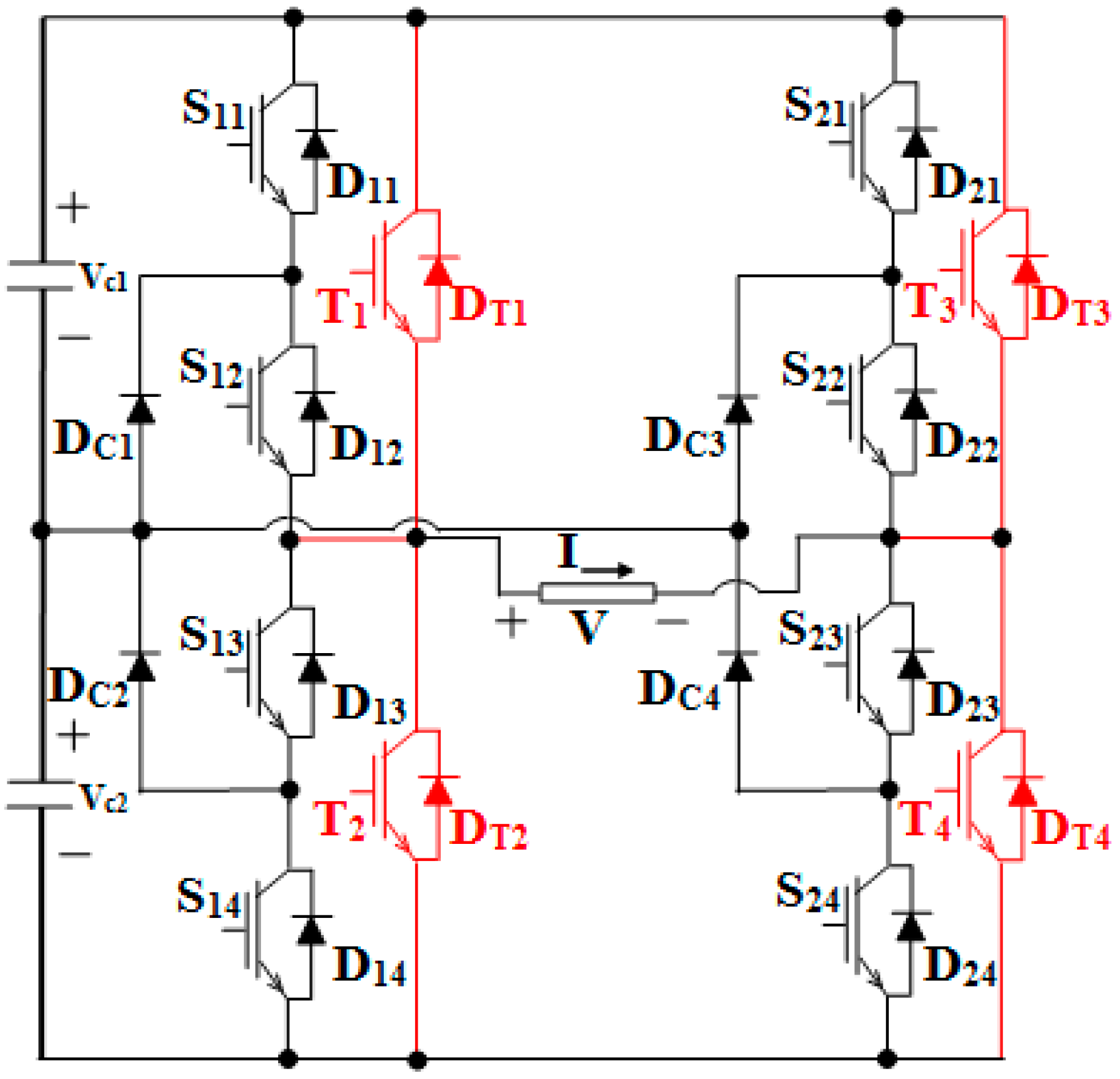
Figure 1b. As mentioned in the previous section, there is no bidirectional switch between the phases, as well as in each single-phase NPC module. Hence, the fault-tolerant operation in each phase is ensured independently of those in the other two phases. In this regard, acquiring fault-tolerant operation is investigated in this paper for a single-phase five-level NPC module. The proposed fault-tolerant topology is represented in
Figure 2. As can be seen, the redundant components (T
1, D
T1), (T
2, D
T2), (T
3, D
T3), and (T
4, D
T4), indicated by the red color, are permanently inserted in the circuit. In healthy operation, any command signal is not applied to these redundant switches. The components conducting in each switching state and the corresponding switching pattern are tabulated in
Table 2 and
Table 3, respectively. The rows highlighted in gray in
Table 2 and
Table 3 (from switching state 10 to 17) are exclusively used during open-switch fault-tolerant operation. It should be noted that redundant anti-parallel diodes (D
T1, D
T2, D
T3 and D
T4), even in healthy operation, contribute to form the current path. Not only does this matter not cause any problem, but it also provides redundancy for the main anti-parallel diodes (D
11, D
12, D
13, D
14, D
21, D
22, D
23 and D
24), because according to
Table 2, a redundant anti-parallel diode always conducts in parallel with two main anti-parallel diodes located in the same half-leg. It should be noted that in the case of a fault event in a main anti-parallel diode, the fault-tolerant operation is immediately realized without fault diagnosis because in this case, the current flows through the corresponding redundant anti-parallel diode.
In order to realize fault-tolerant operation in the case of a fault event in a clamping diode, any redundant switch is not required. In this case, the remedial operation is exclusively carried out by modifying the switching commands. In order to acquire open-switch fault-tolerant operation, using the redundant switches is indispensable.
4. Simulation Results
The simulation results are represented in the two following subsections. In the first one, the simulation results concerning the open-clamping diode fault-tolerant operation are provided and discussed. In the second one, the simulation results regarding the fault-tolerant strategy in case of a fault event in a power switch are presented. Since the topology of the converter is symmetric, clamping diode DC4 and switches S11 and S12 are chosen as the faulty components. The load resistance, the load inductance, the switching frequency, the fundamental frequency, the DC link capacitors, the DC link voltage and the modulation index are set at 27.7 Ω, 9 mH, 1 kHz, 50 Hz, 2.2 mF, 50 V and 0.8, respectively. These values are set based on the available hardware in our laboratory.
Matlab/Simulink environment was used to carry out the simulations. The fixed step method (step of 1 µs) has been set.
4.1. Remedial Operation in the Case of a Fault Event in a Clamping Diode
The proposed open-clamping diode fault-tolerant strategy does not require any additional or redundant component. Solely by modifying the infeasible switching states applied in healthy operation (see
Table 4), service continuity is ensured.
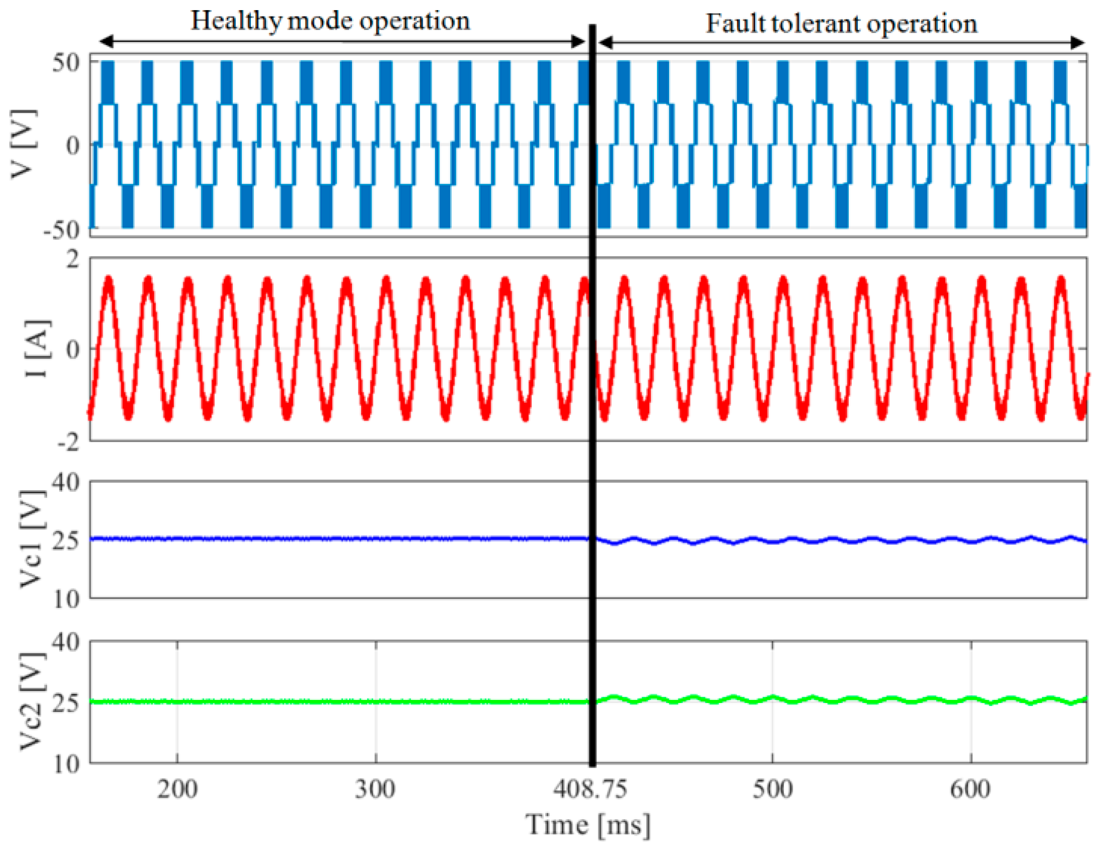
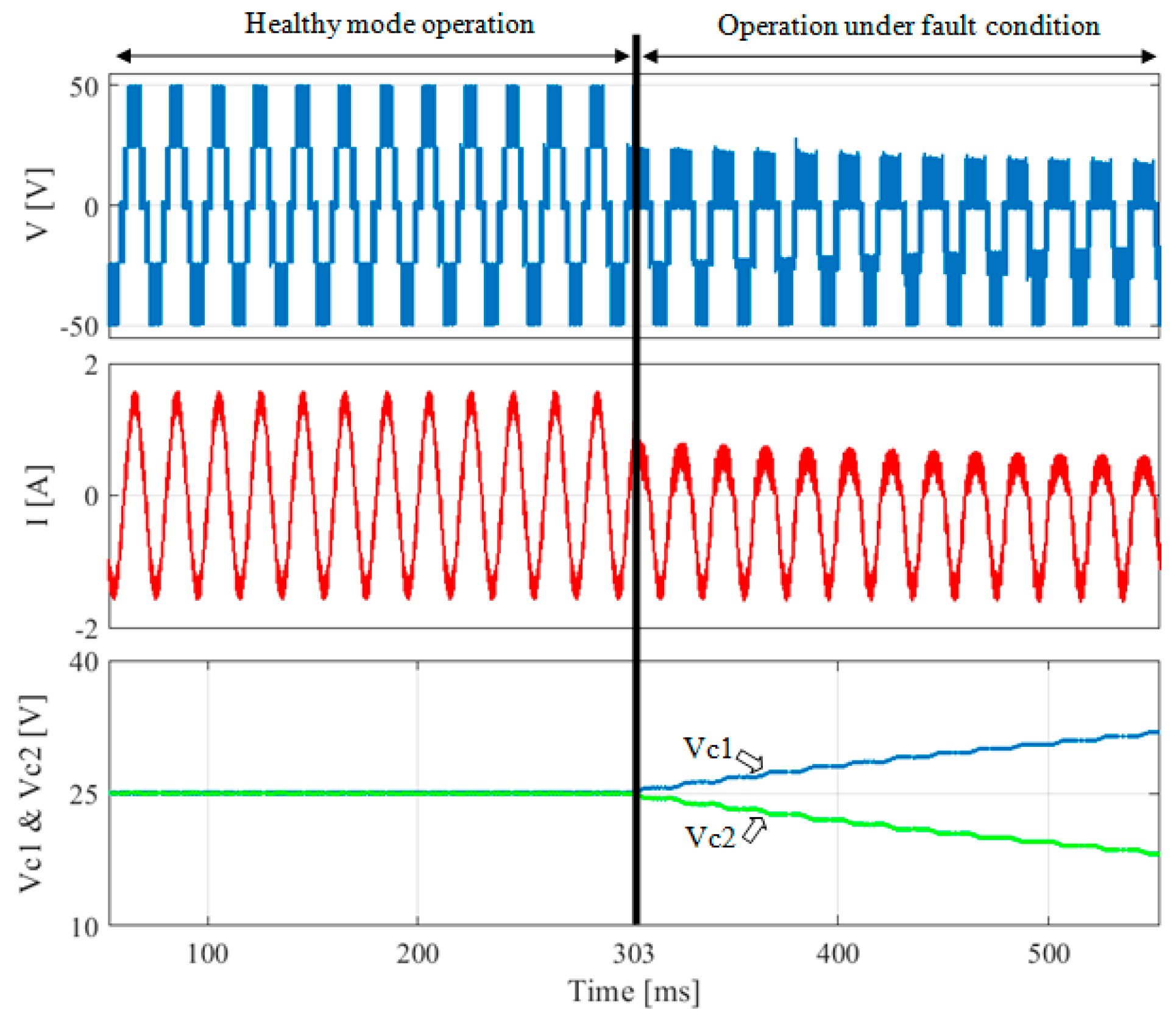
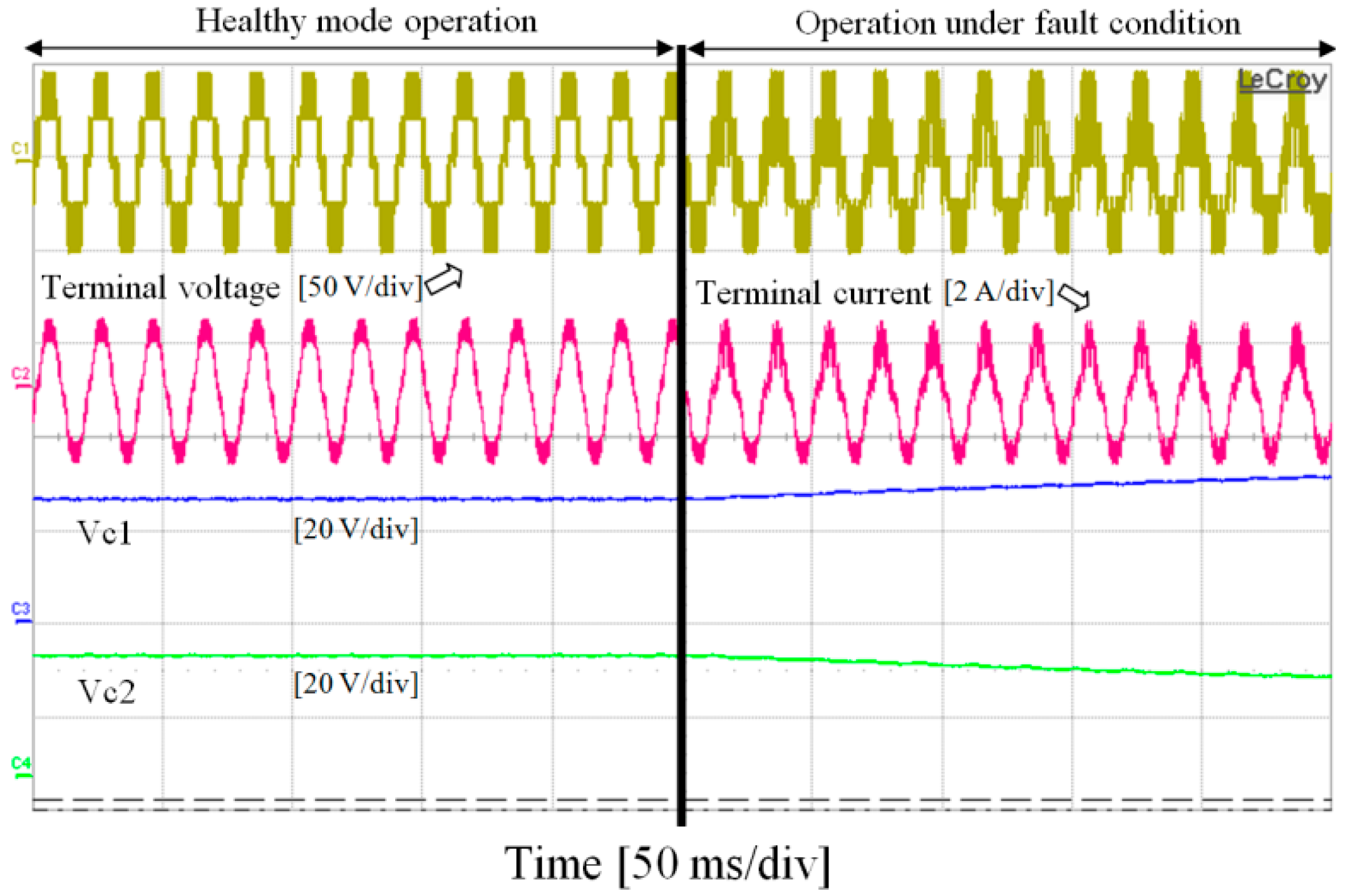
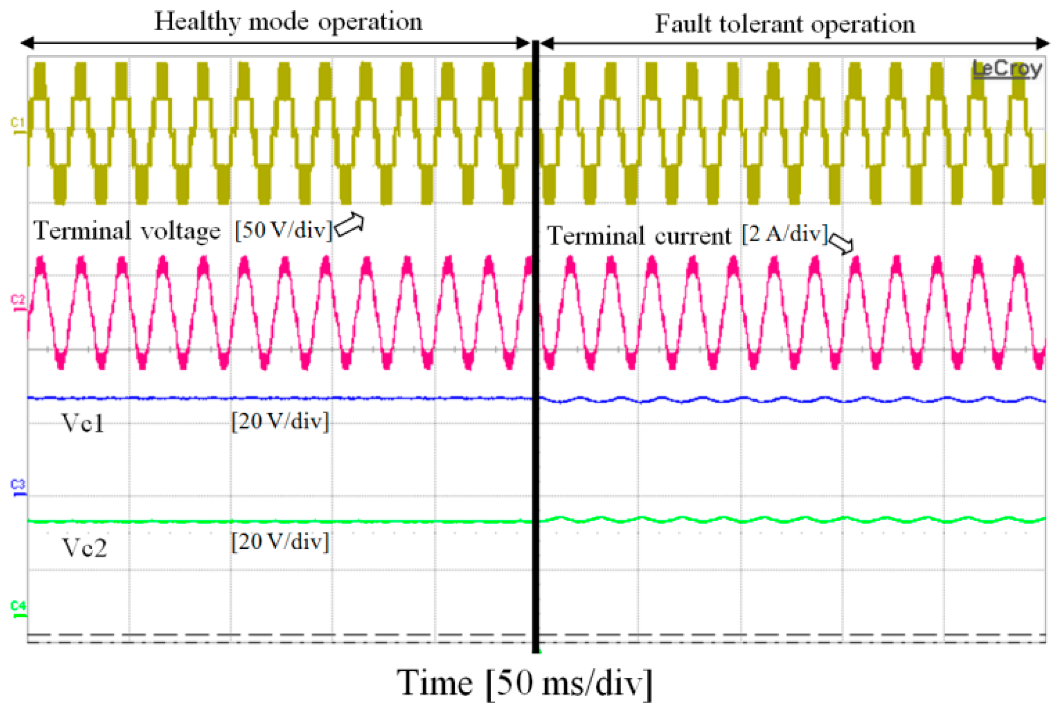
Figure 3 represents the inverter operation in the case of an open-circuit fault occurrence in DC4 without applying fault-tolerant strategy. As can be seen, once the fault occurs, the two DC link capacitors’ voltages start to diverge from their rated values in such a way that one of them attains entire DC link voltage and the other one would be discharged completely. Thus, one of the capacitors would be exposed to overvoltage. Furthermore, after the fault event, the terminal voltage and current are deteriorated in terms of distortion. The outcomes of the applied fault-tolerant strategy (in case of a fault event in DC4) are illustrated in
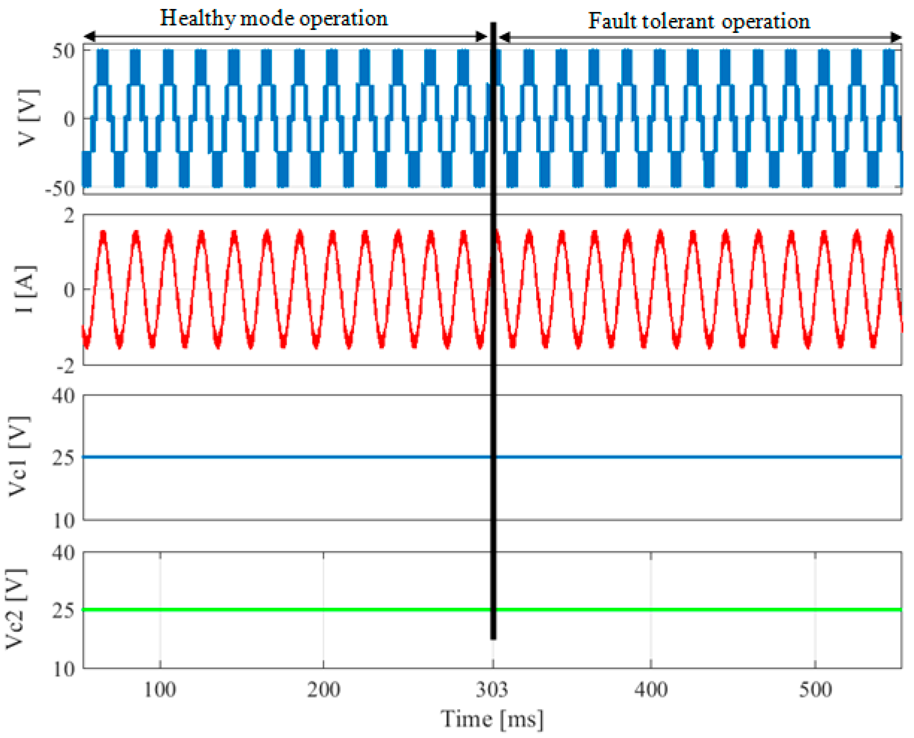
Figure 4 and
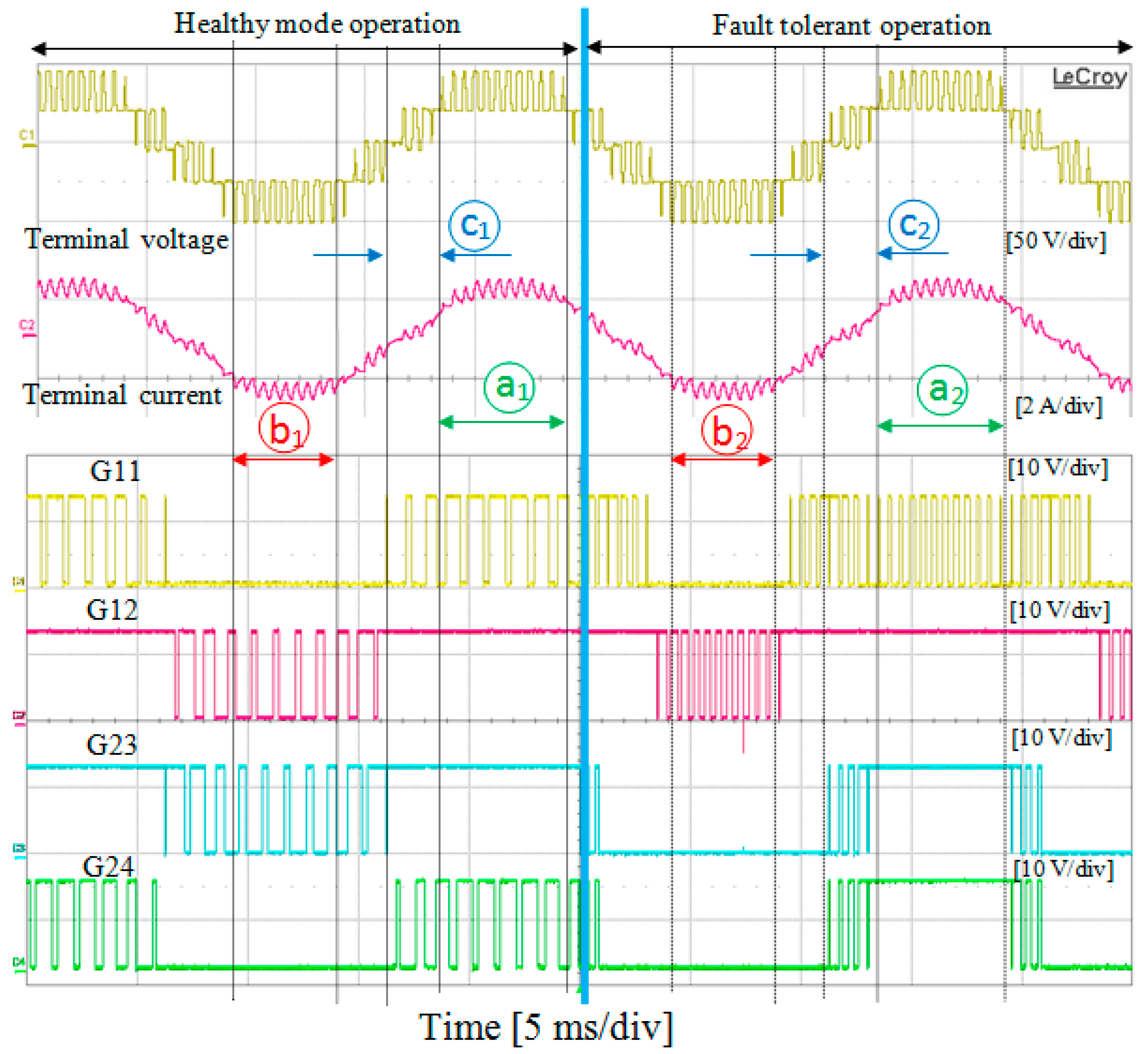
Figure 5. As shown in
Figure 4, by applying the fault-tolerant strategy, the terminal and current voltage obtained during fault-tolerant operation are identical to those obtained during healthy operation.
Moreover, despite low frequency oscillation with negligible ripple amplitude (around 1.5 V peak to peak) in the DC link capacitors’ voltages, the neutral point voltage is stabilized. In
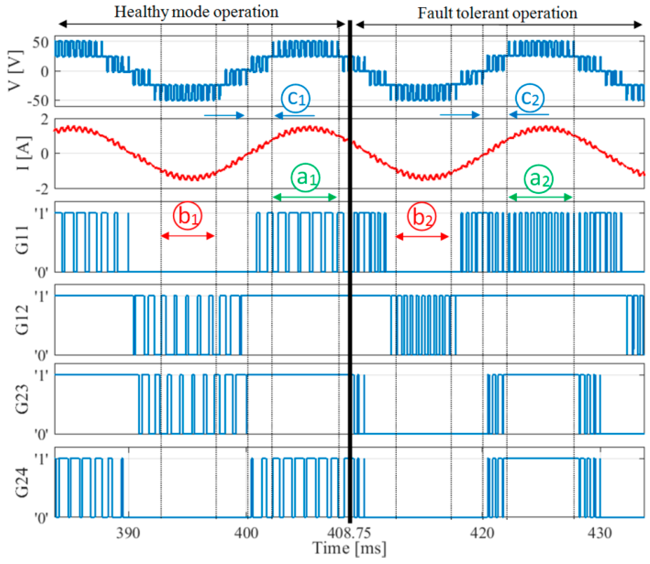
Figure 5, by comparing the healthy operation with the fault-tolerant operation of the inverter (in case of a fault event in DC4), the modifications of the switching states are represented. In this regard, the switching states corresponding to the same voltage levels (healthy operation and fault-tolerant operation) obtained at the terminal are compared. In
Figure 5, four gate signals comprising G11 (gate signal of S
11), G12 (gate signal of S
12), G23 (gate signal of S
23) and G24 (gate signal of S
24) are selected to represent the applied switching states. Gate signals applied to S
13, S
14, S
21 and S
22 are complementary to those corresponding to S
11, S
12, S
23, and S
24, respectively (see
Table 3). Thus, from the four mentioned gate signals, the corresponding switching state is determined. In interval a
1, the voltage levels made at the terminal in healthy mode are +Vdc and +Vdc/2. According to the gate signals and
Table 3, switching states 1, 2 and 3 are applied in this interval. In interval a
2, the same terminal voltage levels are obtained compared with interval a
1 but the switching state 2 is substituted by switching state 3. In fact, over entire interval a
2, G12, G23 and G24 are set at ‘1’ and solely G11 is toggled between ‘0’ and ‘1’ which complies with
Table 4, according to the switching patterns provided in
Table 3 for switching states 1, 2 and 3. In interval b
1 the terminal voltage levels −Vdc and −Vdc/2 are achieved. Based on the represented gate signals in interval b
1 and
Table 3, switching states 7, 8 and 9 are applied in this interval. By performing a detailed comparison between the gate signals applied in interval b
2 (fault-tolerant operation) with those applied in interval b
1, one can deduce that switching state 8 is replaced by switching state 7 (G11, G23 and G24 are set at ‘0’ and G12 is toggled between ‘0’ and ‘1’) which conforms to the data provided in
Table 4. Likewise, by comparison of interval c
1 with interval c
2, it is deduced that during fault-tolerant operation, switching states 2 and 5 are substituted by switching states 3 and 4, respectively.
4.2. Fault-Tolerant Operation in Case of Fault Event in a Switch
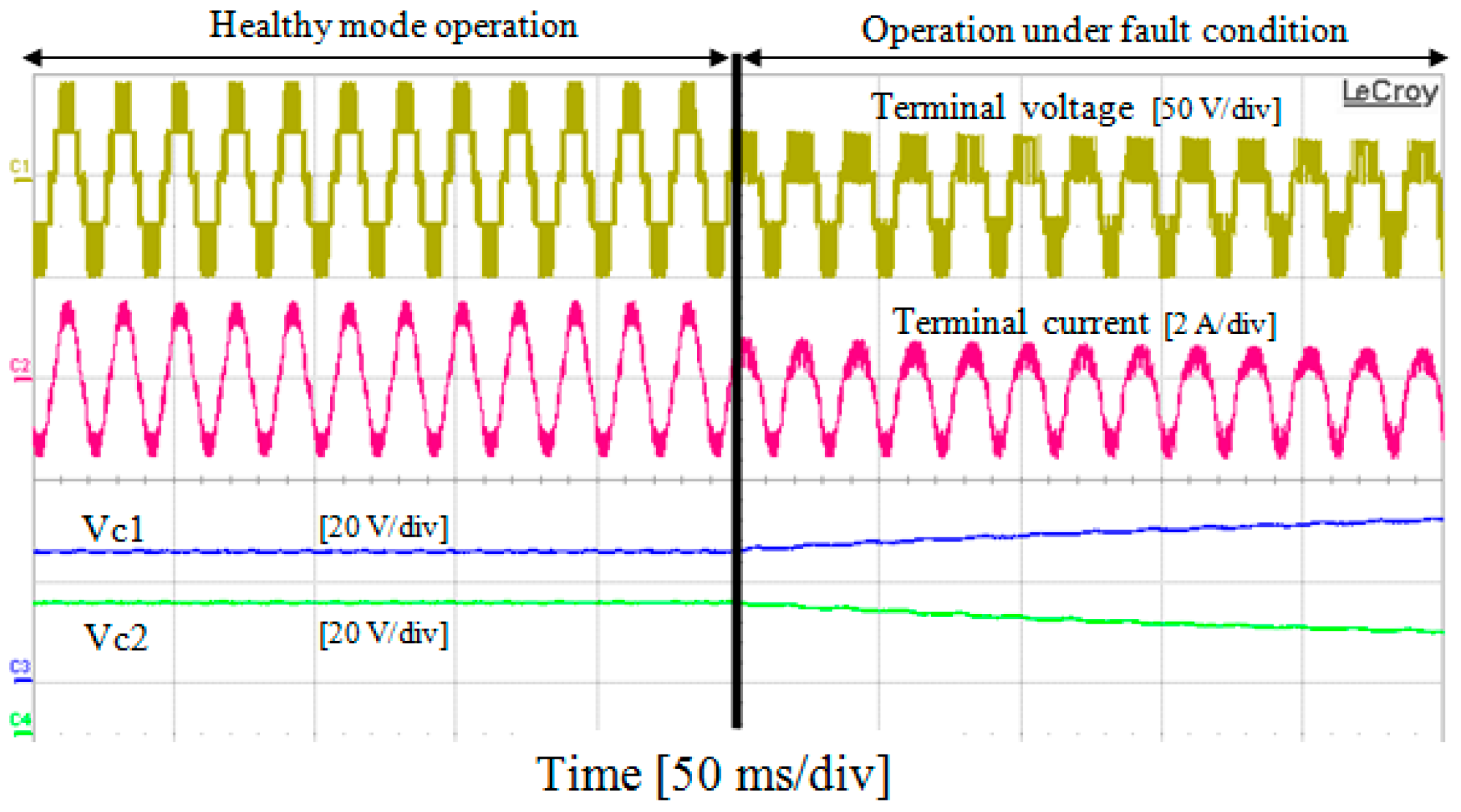
As can be seen in
Figure 6, subsequently to fault generation in S
11, the voltage level +Vdc is no longer achievable. Furthermore, the DC link capacitors’ voltages diverge from their rated value. As can be observed in
Figure 7, by applying fault-tolerant strategy subsequently to the fault occurrence, the rated current as well as the rated voltage are acquired, which are identical to those in healthy operation.
Furthermore, the DC link capacitors’ voltages are stabilized at their rated value during fault-tolerant operation.
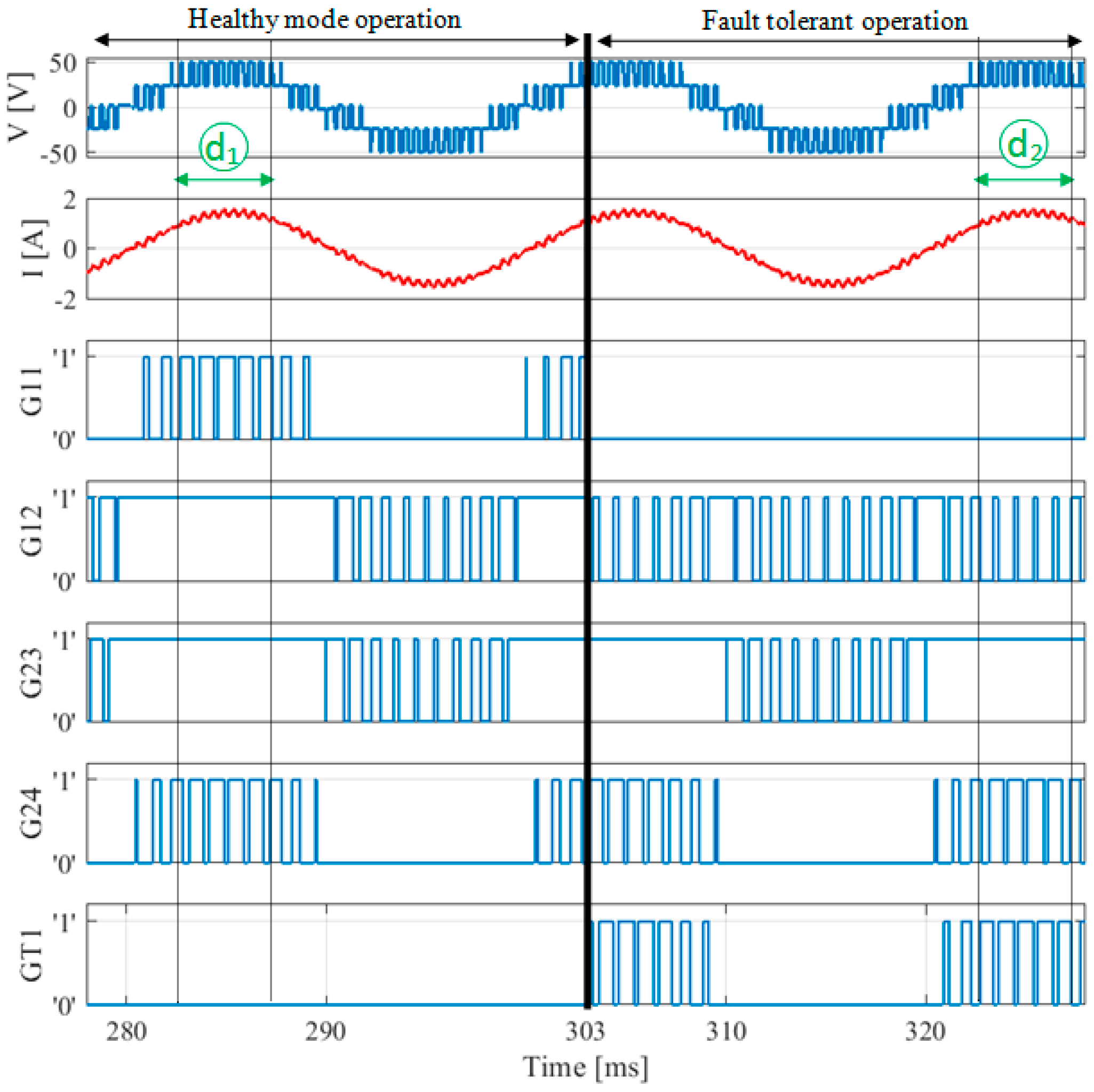
Figure 8 represents the applied gate signals during healthy and fault-tolerant operation, allowing us to observe the modification of switching states due to the applied fault-tolerant strategy. During interval d
1, command signals G12, G23 and GT1 (gate signal of T
1) are set at ‘1’, ‘1’ and ‘0’, respectively, and gate signals G11 and G24 toggle between ‘0’ and ‘1’. Thus, in accordance with the data tabulated in
Table 3, it is deduced that switching states 1, 2 and 3 are applied during interval d
1. To observe the modification of the switching states due to the fault-tolerant strategy, interval d
2, during which the terminal voltage and current are identical to those in interval d
1, is chosen. According to
Figure 8, during interval d
2, gate signals G11 and G23 are set at ‘0’ and gate signals G12, G24 and GT1 toggle between ‘0’ and ‘1’. Thus, by referring to
Table 3, it is deduced that the switching states 3, 10 and 11 are applied during this interval. Hence, by comparing the switching states applied during interval d
1 (healthy operation) with those applied during interval d
2 (fault-tolerant operation), it is concluded that switching states 1 and 2 are replaced by switching states 10 and 11, which complies with the data provided in
Table 4 (the row corresponding to faulty switch S
11).
In this research work, the classical pulse-width modulation (PWM) method has been adopted. However, it should be noted that the proposed strategy is valid for all types of modulation strategies.
As discussed in the paper, the proposed structure associated with the fault-tolerant approach is able to restore nominal operation during fault-tolerant operation in case of a fault event in a switch or diode. Since nominal operation is perfectly restored during fault-tolerant operation, this approach cannot be assessed numerically or quantitatively.
During healthy operation, the total harmonic distortion (THD) of the terminal current is 8.5%. In case of a fault event in DC4, without applying the remedial control, the THD of the terminal current reaches 21%. By applying the remedial control, the THD value of the terminal current attains 8.5%.
In case of a fault occurrence in S11, without applying the remedial control and reconfiguration, the THD of the terminal current reaches 25%. During fault-tolerant operation, the THD value of the terminal current reaches the level obtained during healthy operation.
