Article

Electric Field Distribution and Dielectric Losses in XLPE Insulation and Semiconductor Screens of High-Voltage Cables

Division of High Voltage and Electrotechnical Materials, Institute of Electric Power Engineering, Faculty of Environmental Engineering and Energy, Poznan University of Technology, 60-965 Poznan, Poland
Energies 2022, 15(13), 4692; https://doi.org/10.3390/en15134692
Submission received: 31 May 2022 / Revised: 21 June 2022 / Accepted: 23 June 2022 / Published: 26 June 2022
(This article belongs to the Special Issue Advanced Research of High Voltage Insulation)

Abstract

:
This article presents the electric field distribution E and dielectric losses ΔPdiel. in the insulation system of high-voltage cables. Such a system consists of inner and outer semiconductor screens and XLPE insulation. The aim of this study was to compare the values of E and ΔPdiel. between semiconductor screens and XLPE insulation. The objects of the research were high-voltage cables of 110 kV, 220 kV, 400 kV, and 500 kV. The geometrical dimensions of the cables, especially the radii of individual layers of insulation, as well as the electrical properties of the screens and XLPE, were taken from the literature. Semiconductor screens and XLPE insulation were treated as a system of three concentric cylinders. When determining the electric field distribution, both the electrical permittivity and electrical conductivity, which, in the case of semiconductor screens, play important roles, were taken into account. The obtained results prove that both the electric field distribution E and dielectric losses Pdiel. are significantly larger in XLPE insulation than in semiconductor screens. The intensity E in XLPE insulation is about four orders of magnitude greater than the intensity in semiconductor screens. Dielectric losses ΔPdiel. in XLPE insulation are about eight orders of magnitude greater than the losses occurring in semiconductor screens.

1. Introduction

Cross-linked polyethylene (XLPE) is the most commonly used material in the insulation system of high-voltage cables. Despite the relatively short duration of XLPE use, this material is one of the most recognized materials used in high-voltage insulation systems. There have been countless scientific articles describing the various properties of XLPE, such as mechanical, chemical, physical, and thermal properties, but, above all, its electrical properties. Scientists have analyzed the impacts of temperature, frequency, water, nanoparticles, and electric stress on properties such as electrical permittivity, electrical conductivity, and tan(delta). Additionally, the influence of the aforementioned factors on thermal conductivity, space charge density, breakdown voltage, activity of partial discharges, and dielectric losses has also been investigated.
In papers [1,2,3,4,5,6,7,8,9,10,11,12,13,14,15,16,17,18,19,20,21] the authors described the effect of selected factors on the electrical permittivity ε of XLPE. These factors most often include frequency, but also include the XLPE aging time, temperature, and insulation thickness.
Many articles have described the effect of various factors on the electrical conductivity γ of cross-linked polyethylene [1,4,5,6,7,9,10,11,12,18,21,22,23,24,25,26,27,28,29,30,31,32,33,34,35,36,37,38,39,40,41,42]. These factors include electric field stress, percentage of nanoparticles (most commonly Al2O3), distance from the high-voltage conductor, temperature, aging time, degassing time, frequency, and insulation thickness.
The most-studied property of XLPE is its dielectric loss coefficient tan(delta) [2,4,8,9,12,13,14,15,16,17,18,19,20,21,23,27,33,34,39,41,42,43,44,45,46,47,48,49,50,51,52,53,54,55,56,57,58]. Authors have analyzed the effects of frequency, aging time, cable life, voltage test, and temperature on the tan(delta) distribution and value.
Relatively little attention has been paid to electric field distributions and dielectric losses in XLPE insulation. In the scientific literature, we can find only a few articles from the last few decades referring to these topics. This remark applies especially to semiconductor screens located directly in pure XLPE insulation.
The electric field distribution in the insulation of a high-voltage cable plays an important role in the context of its reliable and long-term operation. Of particular importance is the maximum value of electric field stress Emax. An underestimated maximum value can consequently lead to the rapid development of partial discharges, which can cause the cable to fail. In the case of high-voltage cables, electrical insulation usually consists of main insulation (XLPE) and semiconductor screens whose task it is to properly control (reduce) the electric field stress in the area of the high-voltage and return conductors. When determining the electric field distribution, a certain simplification is usually used, assuming that the main insulation (XLPE) and semiconductor screens have the same electrical properties (electrical permittivity and electrical conductivity) that have an impact on electric field stress. Meanwhile, these properties can differ significantly, which influences the values of electric field stress in the main insulation (XLPE) and semiconductor screens.
Dielectric losses in the insulation of high-voltage cables are manifested in the form of thermal energy, which can lead to the deterioration of many of the electrical properties of insulation, such as electrical resistivity, electrical strength, and the dielectric loss coefficient. Few scientific centers have conducted research on dielectric losses in the insulation of high-voltage cables. A few studies on this subject used a simplification that did not distinguish between the dielectric losses that are emitted in the main insulation (XLPE) and semiconductor screens.
In article [5], the authors presented the voltage distribution in pure XLPE insulation and semiconductor screens for 320 kV and 500 kV high-voltage cables. The distribution showed that the authors made a simplification, assuming that the distributions of the potential, and thus the electric field stress, in both semiconductor screens and pure XLPE, were similar. Thus, the authors did not take into account the differences between the properties of the semiconductor screens and pure XLPE that determine the electric field distribution and dielectric losses. The maximum value of electric field stress for a 320 kV cable was equal to 17 kV·mm−1, and for a 500 kV cable, Emax = 18 kV·mm−1.
In papers [5,15,58,59], the authors, determining the losses in cable insulation, analyzed only the losses in XLPE insulation, omitting losses in semiconductor screens. In publication [15], the authors presented the results of the analysis of dielectric losses for a 30 kV cable. The value of these losses for that type of high-voltage cable was equal to 250 W·km−1. In publication [59], the authors presented the results of calculations of dielectric losses for a 110 kV cable, which amounted to 239 W·km−1. In publication [5], the authors presented the results of calculations of dielectric losses in the insulation of 320 kV and 500 kV cables. These losses amounted to 60 and 100 W·km−1, respectively. In publication [58], the authors presented dielectric losses not depending on the voltage, but depending on electric field stress equal to 5, 10, and 15 kV·mm−1, which, according to the author, may correspond to cables with voltages in the range of 200 kV to 500 kV. These losses were equal to 1000, 2000, and 4000 W·km−1, respectively. As you can see, there are significant discrepancies in the presented values of dielectric losses. For example, for a 110 kV cable, the dielectric losses exceed 200 W·km−1 [59], and for a 500 kV cable, the losses are only 100 W·km−1 [5].
In article [50], the authors, determining the financial costs that result from losses in cable insulation, focused only on losses in XLPE insulation. In article [52], the authors described the effect of semiconductor screens on losses in cables. However, the considerations ended with the analysis of the tan(delta) coefficient, without specifying the impact of semiconductor screens on the value of losses expressed in Watts.
In summary, it is difficult to find research results showing the electric field distributions and dielectric losses in cable insulation that would take into account the differences between the properties of semiconductor screens and pure XLPE. For this reason, the author of this article fills this gap.
The electric field distribution in series-stratified insulation systems depends on the relationship between the electrical permittivity and electrical conductivity of the materials from which the individual layers are designed. The permittivity and the conductivity of the semiconductor screens are significantly higher than the permittivity and the conductivity of pure XLPE. This means that the electric field will be displaced from the semiconductor screens to pure XLPE. Therefore, the author puts forward the thesis that the electric field stress in semiconductor screens will be much smaller than that in pure XLPE.
Dielectric losses in an insulating material depend on a number of factors, such as the electric field stress (square dependence), pulsation, electrical permittivity, and dielectric loss coefficient tan(delta). The greater these properties, the greater the dielectric losses. It is true that the permittivity and tan(delta) of semiconductor screens are greater than those of pure XLPE. However, the electric field stress in pure XLPE is probably much higher than that in semiconductor screens. Therefore, the author puts forward the thesis that dielectric losses in semiconductor screens will be significantly lower than those in pure XLPE.

2. Materials and Methods

2.1. Materials

The electric field distribution E and dielectric losses ΔPdiel. were determined for four typical voltage values: 110 kV, 220 kV, 400 kV, and 500 kV (phase-to-phase voltage).
The author’s intention was not to analyze the electric field distribution and dielectric losses for the selected cable manufacturer. Therefore, the geometrical parameters of the cables (Table 1) and the properties of the semiconductor screens and XLPE insulation (Table 2) were taken from the rich scientific literature.
On the basis of the data in Table 1, it is possible to determine the thickness of the inner semiconductor screen (R1–R0), XLPE insulation (R2–R1), and the outer semiconductor screen (R3–R2). The voltage values given in Table 1 are the phase-to-phase voltages. When determining the electric field distributions and dielectric losses, the phase voltage values were used.

2.2. Methods

2.2.1. Calculation of Electric Field Distribution

The electric field distribution E between two concentric cylinders is described by a well-known formula [15,34]:
E = U r · ln ( r i + 1 r i )
where: U—phase voltage (V), r—distance from the center of the cylinder (m), ri < r < ri+1, ri+1—radius of the larger cylinder (m), and ri—radius of the smaller cylinder (m).
For a larger number of layers, designed from different insulating materials, the following formula is used [62,63,64]:
E k ( r ) = U r · ( ω · ε k ) 2 + ( γ k ) 2 · i = 1 n ln ( r i + 1 r i ) ( ω · ε i ) 2 + ( γ k ) 2
where: Ek(r)—electric field stress in layer k (V·m−1), U—phase voltage (V), ω—pulsation (1·s−1), εk—absolute electrical permittivity of the material of layer k (F·m−1) (ε = εo·εr, εo—absolute electrical permittivity of vacuum equal to 8.85 × 10⁻¹² F·m−1 and εr—relative electrical permittivity of the insulating material), γk—electrical conductivity of layer k (S·m−1), ri+1—outer radius of layer i (m), ri—inner radius of layer i (m), εi—absolute permittivity of layer i (F·m−1), and γi—electrical conductivity of layer i (S·m−1). In the analyzed case, there were three layers (the inner layer of the semiconductor screen, XLPE insulation, and the outer layer of the semiconductor screen). Thus, i = 1, 2, and 3, while n = 3.
In insulating systems layered in series, the equation describing the electric field distribution in individual layers usually takes into account only the different permittivities of insulating materials. This situation occurs when the electric field distribution is capacitive. A capacitive field occurs when the electrical conductivity of insulating materials is relatively small and the condition is met:
ω · ε γ
This is the most common case in insulation systems designed from materials with very high electrical resistivity.
Table 3 shows the parameters ω·ε and γ for the semiconductive material and XLPE insulation for frequency f = 50 Hz. In the case of cross-linked polyethylene, ω·ε is actually 4 orders of magnitude greater than the electrical conductivity γ. In this case, the resistive field may be ignored. However, in the case of a semiconductive material, the parameter ω·ε is as much as 5 rows smaller than γ. This means that the electric field distribution in the semiconductive material will be resistive. For the above reasons, the author decided to take into account both the electrical permittivity and electrical conductivity of both insulating materials.

2.2.2. Calculation of Dielectric Losses

The dielectric losses in insulation systems shall be determined using the following formula [15,58,59]:
Δ P diel . = ε · C · U 2 · tan ( delta ) · L
where: ΔPdiel.—dielectric losses (W), ε—absolute electrical permittivity of the insulating material (F·m−1), U—phase voltage (V), C—electrical capacity of cable insulation (F), tan(delta)—dielectric loss coefficient (-), and L—cable length (m).
On the basis of Formula (4), it can be concluded that losses should be determined separately for the three analyzed layers. This involves the determination of three voltage drops, giving the total U value, in three individual layers, which is quite a difficult task. The three C capacitance values should also be determined for each layer. For this reason, the author proposes to use a different version of Formula (4) to determine dielectric losses [65]:
Δ p diel . = E 2 · ω · ε · tan ( delta )
where: Δpdiel—unit dielectric losses in the insulating material (W·m−3), E—electric field stress (V·m−1), ω—pulsation (1·m−1), ε—absolute electrical permittivity of the insulating material, and tan(delta)—coefficient of dielectric losses of the insulating material.
Formula (5) describes the dependence of the unit dielectric losses on the electric field E in individual layers, and not on the voltage and capacitance drop of the individual layers. One of the objectives of the research is to determine the electric field distribution in the analyzed layers, as described in Section 2.2.1. Thus, determining dielectric losses using Formula (5) is a simpler task compared with Formula (4).
After substituting Formula (2), describing the electric field distribution, to Formula (5), we get the formula:
Δ p diel . k ( r ) = ( U r · ( ω · ε k ) 2 + ( γ k ) 2 · i = 1 n ln ( r i + 1 r i ) ( ω · ε i ) 2 + ( γ k ) 2 ) 2 · ω · ε k · tan ( delta ) k
Formula (6) describes the unit losses Δpdiel.k for the k layer, expressed in W·m−3. Thus, this formula should be integrated into region V described in the cylindrical coordinates r ϵ (ri, ri+1), φ ϵ (0, 2π), and z ϵ (0, L) to obtain a final formula for dielectric losses in three analyzed layers. Since Formulas (5) and (6) are expressed for the Cartesian system, the Jacobian J should be used to change from the Cartesian to the cylindrical system (J = r).
Δ P diel . k = V k ( U r · ( ω · ε k ) 2 + ( γ k ) 2 · i = 1 n ln ( r i + 1 r i ) ( ω · ε i ) 2 + ( γ k ) 2 ) 2 · ω · ε k · tan ( delta ) k · r · dr · d φ · dz
After simplification, we get the formula:
Δ P diel . k = V k ( U ( ω · ε k ) 2 + ( γ k ) 2 · i = 1 n ln ( r i + 1 r i ) ( ω · ε i ) 2 + ( γ k ) 2 ) 2 · 1 r · ω · ε k · tan ( delta ) k · dr · d φ · dz
After integration, we get the final formula for dielectric losses in individual layers:
Δ P diel . k = ( U ( ω · ε k ) 2 + ( γ k ) 2 · i = 1 n ln ( r i + 1 r i ) ( ω · ε i ) 2 + ( γ k ) 2 ) 2 · ln ( r i   + 1 r i ) · ω · ε k · tan ( delta ) k · 2 · π · L

3. Results and Discussion

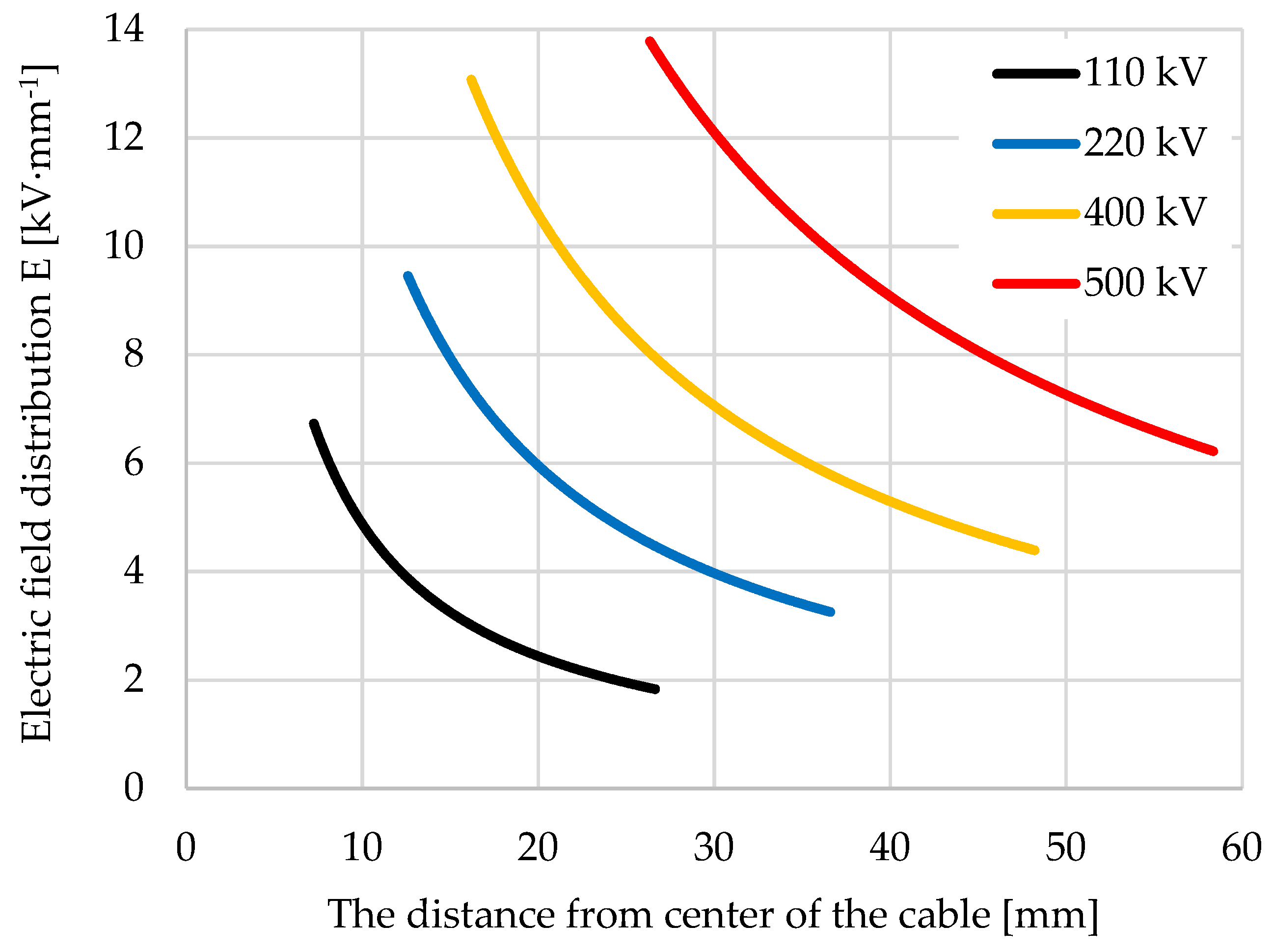
3.1. Electric Field Distribution in Semiconductor Screens and XLPE Insulation in High-Voltage Cables

On the basis of Formula (2), the electric field distributions E in the three analyzed layers (inner semiconductor screen, XLPE insulation, and outer semiconductor screen) for four voltage values of 110, 220, 400, and 500 kV were determined. The electric field distribution in the individual layers differed significantly. The values of electrical field stress in the semiconductor screen were about four orders of magnitude lower than the intensity in XLPE insulation, which proves the thesis put forward by the author. For this reason, it was decided to present the results of the calculations only in a table that contains the maximum Emax and minimum Emin values of electric field stress in the analyzed layers (see Table 4). The graph of the electric field distribution in the three analyzed layers would be illegible due to the very large differences in values. The values of the electric field stress E in the inner semiconductor screen were about three times greater than those of the stress E in the outer semiconductor screen.
Based on the obtained results, it can be concluded that, as the distance from the high-voltage conductor increased, the electric field stress E in all three analyzed layers decreased. As the cable voltage U increased, the values of the electric field stress E also increased.
The values of electric field stress in semiconductor screens were about four orders of magnitude lower than those of the stress E in XLPE insulation. Thus, the thesis has been proven that the electric field stress in semiconductor screens would be much lower than the stress E in XLPE insulation. The stress E in semiconductor screens was equal to thousandths of parts kV·mm−1, and in XLPE insulation, it was several kV·mm−1. This is certainly due to the very large difference in electrical conductivity γ, which, for semiconductor screens, was about nine orders of magnitude larger than that in XLPE (Table 3). This resulted in the displacement of the electric field from the semiconductor screens to the XLPE insulation. In contrast, the difference in electrical permittivity ε was equal to one order of magnitude and did not have a significant impact on the electric field distribution. Therefore, it was right to assume that the analyzed electric field distribution would be resistive–capacitive.
If we assume that the electric field distribution in the analyzed layers is only capacitive, as can be found in the literature, then the electric field stress E in semiconductor screens would be about 10 times lower than the intensity E in XLPE insulation. Thus, the results obtained would be wrong.
Figure 1 shows the electric field distributions E for four cable voltage values U only in XLPE insulation. The E values decreased as the distance from the high-voltage conductor and the voltage of the cable increased. The maximum values Emax were rounded to 7 kV·mm−1 (110 kV), 10 kV·mm−1 (220 kV), 13 kV·mm−1 (400 kV), and 14 kV·mm−1 (500 kV).
There is some coincidence between the obtained results and the data contained in the literature. In article [5], the authors provided the maximum values of electric field stress for a 500 kV cable (Emax = 18 kV·mm−1) and for a 320 kV cable (Emax = 17 kV·mm−1). Meanwhile, the Emax obtained in these investigations for a 500 kV cable was about 14 kV·mm−1, and for 220 kV and 400 kV cables, the maximum value of electric field stress was equal to 10 and 13 kV·mm−1, respectively. Some differences may have resulted from the different geometric dimensions of the cables.

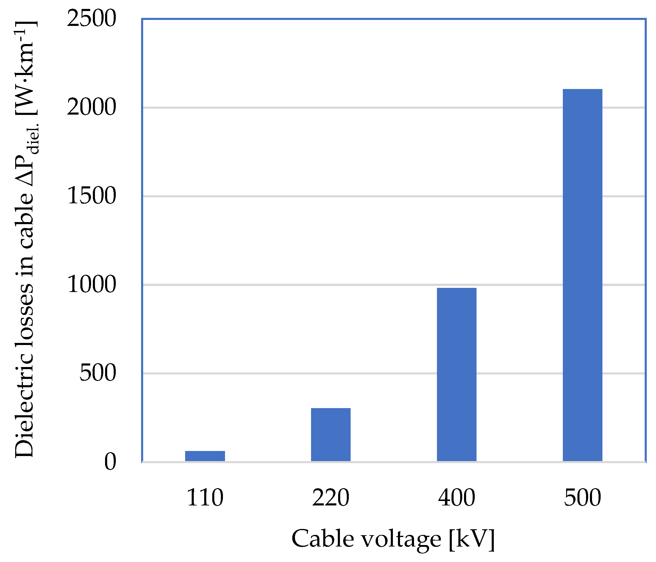
3.2. Dielectric Losses in Semiconductor Screens and XLPE Insulation of High-Voltage cables

Table 5 shows the determined dielectric losses in the analyzed layers of high-voltage cables, based on Formula (9). A cable length of 1000 m (1 km) was assumed. As the cable voltage increased, losses increased both in the semiconductor screens and XLPE insulation.
Losses in semiconductor screens were about nine orders of magnitude lower than the losses in XLPE insulation. The reason for this was the much lower electric field stress E in semiconductor screens compared with the intensity E in XLPE (Table 4). The intensity E in the semiconductor screens was four orders of magnitude less than that in XLPE. Dielectric losses depend on the square of the electric field stress (Formula (5)). Therefore, losses in semiconductor screens were about nine orders lower than those in XLPE. Losses in semiconductor screens were equal to millionths of watts, and in XLPE, these losses were equal to a dozen to several thousand watts. This means that the thesis that dielectric losses in semiconductor screens will be much smaller than those in XLPE has been proven.
Figure 2 shows dielectric losses only in XLPE insulation depending on the cable voltage. These losses increased with the increase in cable voltage from several dozen to two thousand watts. The increase in losses was approximately proportional to the square of the increase in cable voltage, which is consistent with Formula (9).
Comparing the obtained results with data from the literature, it can be said that there were some discrepancies. In publication [59], the authors determined the dielectric losses for a 110 kV cable, which were equal to 239 W·km−1. Meanwhile, in this study, the losses for the 110 kV cable were several times lower, equal to only 62 W·km−1. In publication [5], the authors presented dielectric losses for a 320 kV cable, which were equal to 60 W·km−1. On the other hand, the results of the loss calculations obtained by the author for 220 kV and 400 kV cables were equal to 304 and 982 W·km−1, respectively. This means that, this time, the obtained results were several times greater. In the same publication [5], the authors gave the dielectric losses for a 500 kV cable, which amounted to 100 W·km−1. Meanwhile, the author obtained a loss value for such a cable equal to over 2000 W·km−1. This means that, this time, the obtained values were higher than the results of other researchers. In turn, in publication [58], the authors gave the value of dielectric losses for a cable in which the maximum electric field stress was equal to 15 kV·mm−1, which allowed us to assume that it was a cable for a voltage of 500 kV. The value of the losses was equal to as much as 4000 W·km−1. Meanwhile, the author obtained a dielectric loss value for a 500 kV cable equal to just over 2000 W·km−1. This means that, this time, the obtained loss values were lower than the literature data.
It can be concluded that there were some discrepancies between the obtained values of dielectric losses compared with the literature data. The obtained loss values were greater or less than the literature data. The reason for this may be the different geometric parameters of the compared cables, which determined, among other things, the electric field stress, which has a significant impact on the value of dielectric losses (quadratic dependence).

3.3. Effect of Electrical Conductivity Not Taking into Account the Electric Field Distribution and Dielectric Losses in Semiconductor Screens and XLPE Insulation of High-Voltage cables

3.3.1. Fundamental Information

In most articles on the electric field distribution E and dielectric losses ΔPdiel. in the insulation of high-voltage cables, the influence of electrical conductivity is ignored. Usually, this approach is right, because the conductivity of insulation materials is very low. However, if semiconductive layers whose electrical conductivity is no longer omitted are analyzed, this property shall be taken into account, as shown in Section 3.1 and Section 3.2.
In this subsection, the author presents the results of calculations of the electric field distribution and dielectric losses in semiconductor screens and XLPE insulation, assuming the existence of only a capacitive field. This means that the effect of electrical conductivity (γ = 0) was omitted. Subsequently, the results obtained, subject to some error, were compared with the results presented in Section 3.1 and Section 3.2.

3.3.2. Electric Field Distributions

The electric field distributions E in semiconductor screens and XLPE insulation were determined from Formula (10). This formula is a form of Formula (2) and determines the electric field distribution assuming that the electrical conductivity γ is zero.
E k ( r ) = U r · ε k · i = 1 n ln ( r i + 1 r i ) ε i
Table 6, as in Table 4, shows the maximum values of Emax and minimum Emin values for individual layers and the voltage values of high-voltage cables. For easy comparison of the results in Table 4 and Table 6, the same units of electric field stress V·m−1 are retained.
Based on the data in Table 6, it can be concluded that the electric field stress in semiconductor layers was about one order of magnitude lower than the intensity E in XLPE insulation. This is consistent with the ratio of electrical permittivity of the semiconductive material (εsemic = 20) and XLPE (εXLPE = 2.3). In the case of a capacitive field only, the electric field distribution in stratified systems is determined only by the ratio of electrical permittivity of individual materials.
Comparing the values of electric field stress in Table 4 and Table 6, it can be concluded that failure to take into account the electrical conductivity γ resulted in an increase in stress E of four orders of magnitude in semiconductor screens and a minimal decrease in stress E in XLPE insulation.

3.3.3. Dielectric Losses

Dielectric losses ΔPdiel. in semiconductor screens and XLPE insulation were determined using the Formula (11), which is a form of Formula (9), for which it was assumed that the electrical conductivity γ = 0.
Δ P diel . k = ( U ε k · i = 1 n ln ( r i + 1 r i ) ε i ) 2 · ln ( r i + 1 r i ) · ω · ε k · tan ( delta ) k · 2 · π · L
Table 7, similar to Table 5, shows the dielectric losses in the analyzed layers of high-voltage cables. Comparing the results in Table 5 and Table 7, it can be concluded that the losses of ΔPdiel. in semiconductor screens increased significantly and were no longer nine orders smaller, but two orders smaller than the losses in XLPE. Losses in XLPE insulation decreased slightly.

4. Conclusions

The electric field stress in the semiconductor screens was four orders of magnitude lower than the intensity E in XLPE insulation. The intensity E in the semiconductor material was equal to thousandths of parts kV·mm−1, and in XLPE, it ranged from a few to a dozen kV·mm−1. The reason for this was the very large differences in electrical conductivity γ of the individual materials. The conductivity of the semiconductor material was nine orders of magnitude greater than that of XLPE. The result was the displacement of the electric field from the semiconductor material to the XLPE.
Dielectric losses ∆Pdiel. in semiconductor screens were nine orders of magnitude lower compared with losses in XLPE insulation. The reason for this was the much lower intensity E in the semiconductor material compared with the intensity E in XLPE, since the losses depend on the square of the electric field stress E.
Dielectric losses ∆Pdiel. in XLPE insulation ranged from several tens to several thousands of watts per km of cable length and should not be neglected in the overall energy balance of high-voltage cable lines. On the other hand, the losses in the semiconductor screens had a very small value, in the order of millionths of watts, and can be omitted from a practical point of view.
Failure to take into account the resistive field had a large impact on the results of the calculations of both the electric field distribution E and dielectric losses ΔPdiel. In this case, the stress E in semiconductor screens was much higher, and slightly lower in XLPE. On the other hand, the losses of ΔPdiel. in semiconductor screens were orders of magnitude larger, and in XLPE insulation, they were slightly smaller.

Funding

This research was financed by the Poznan University of Technology’s financial resources for statutory activity. Number of the project: 0711/SBAD/4514.

Institutional Review Board Statement

Not applicable.

Informed Consent Statement

Not applicable.

Data Availability Statement

Not applicable.

Conflicts of Interest

The author declares no conflict of interest.

References

  1. Vu, T.T.N.; Teyssedre, G.; Le Roy, S. Electric Field Distribution in HVDC Cable Joint in Non-Stationary Conditions. Energies 2021, 14, 5401. [Google Scholar] [CrossRef]
  2. Zhang, Y.; Wu, Z.; Qian, C.; Tan, X.; Yang, J.; Zhong, L. Research on Lifespan Prediction of Cross-Linked Polyethylene Material for XLPE Cables. Appl. Sci. 2020, 10, 5381. [Google Scholar] [CrossRef]
  3. Fabiani, D.; Suraci, S.V. Broadband Dielectric Spectroscopy: A Viable Technique for Aging Assessment of Low-Voltage Cable Insulation Used in Nuclear Power Plants. Polymers 2021, 13, 494. [Google Scholar] [CrossRef] [PubMed]
  4. Plesa, I.; Notingher, P.V.; Stancu, C.; Wiesbrock, F.; Schlögl, S. Polyethylene Nanocomposites for Power Cable Insulations. Polymers 2018, 11, 24. [Google Scholar] [CrossRef] [PubMed] [Green Version]
  5. Diban, B.; Mazzanti, G. The Effect of Insulation Characteristics on Thermal Instability in HVDC Extruded Cables. Energies 2021, 14, 550. [Google Scholar] [CrossRef]
  6. Zhu, G.; Zhou, K.; Gong, W.; He, M.; Kong, J.; Li, K. Inhibition of Rejuvenation Liquid on Trees in XLPE Cables under Switching Impulse Voltages. Energies 2019, 12, 2133. [Google Scholar] [CrossRef] [Green Version]
  7. Qi, H.; Zhank, X.; Wang, R.; Xu, Z.; Wu, Q.; Wang, H.; Li, Z. Effect of Thermal Aging on Direct Current Integrated Charge Characteristics of XLPE Cable Insulation. In Proceedings of the 13th International Conference on the Properties and Applications of Dielectric Materials (ICPADM 2021), Johor Bahru, Malaysia, 11–15 July 2021. [Google Scholar]
  8. Fu, Y.; Wang, X.; Zhao, W.; Wen, Y. Effects of New Photoinitiator on Dielectric Properties of UV-irradiation XLPE. In Proceedings of the 11th International Conference on the Properties and Applications of Dielectric Materials (ICPADM 2015), Sydney, Australia, 19–22 July 2015. [Google Scholar]
  9. Mecheri, Y.; Nedjar, M.; Lamure, A.; Aufray, M.; Drouet, C. Influence of Moisture on the Electrical Properties of XLPE Insulation. In Proceedings of the Conference on Electrical Insulation and Dielectric Phenomena, West Lafayette, IN, USA, 17–20 October 2010. [Google Scholar]
  10. Du, Y.; Geng, P.; Song, J.; Tian, M.; Pang, D. Influence of Temperature and Frequency on Leakage Current of XLPE Cable Insulation. In Proceedings of the IEEE International Conference on High Voltage Engineering and Application (ICHVE), Chengdu, China, 19–22 September 2016. [Google Scholar]
  11. Nejdl, R.; Mentlík, V. Influence of Tools Setting on Processing Quality of XLPE Core Insulation. In Proceedings of the 15th International Scientific Conference on Electric Power Engineering, Brno-Bystrc, Czech Republic, 12–14 May 2014. [Google Scholar]
  12. Wang, X.; Gao, Z.; Zhu, Z.; Li, S.; Liu, Z.; Hao, J.; Ma, Z. Physicochemical and Electrical Property of a New AC 500kV XLPE Submarine Cable Insulation with Different Thermal Aging Condition. In Proceedings of the 12th IEEE International Conference on the Properties and Applications of Dielectric Materials, Xi’an, China, 20–24 May 2018. [Google Scholar]
  13. Yu, L.; Man, X.; Yi, Z.; Darong, X. Study of Structure and Dielectric Property on XLPE/porous-ZnCO3 Composites. In Proceedings of the IEEE International Conference on Solid Dielectrics, Bologna, Italy, 30 June–4 July 2013. [Google Scholar]
  14. Liu, Z.; Gao, Z.; Hao, J.; Liu, C.; Li, H.; Dai, X. Analysis of AC 500kV XLPE Submarine Cable Insulation Laboratory Aging Condition Based on Frequency Domain Dielectric Spectroscopy. In Proceedings of the Electrical Insulation Conference (EIC), Calgary, AB, Canada, 16–19 June 2019. [Google Scholar]
  15. Mecheri, Y.; Medjdoub, A.; Boubakeur, A.; Boujemâa, S. Characterization of Laboratory Aged MV XLPE Cables using Dielectric Losses Factor Measurements. In Proceedings of the 2014 International Conference on Electrical Sciences and Technologies in Maghreb (CISTEM), Tunis, Tunisia, 3–6 November 2014; IEEE: Piscataway, NJ, USA, 2014. ISBN 978-1-4799-7300-2. [Google Scholar] [CrossRef]
  16. Skjølberg, J.; Hvidsten, S.; Farmeo, H. Experience from On-Site Condition Assessment of XLPE MV Cables. In Proceedings of the IEEE International Symposium on Electrical Insulation, Toronto, ON, Canada, 11–14 June 2006. [Google Scholar]
  17. Zhang, Y.; Wu, K.; Zhao, C.; Xiang, J.; Li, J.; Li, S. Non-Debye Dielectric Behavior of Aged XLPE Cable Insulation. In Proceedings of the 12th IEEE International Conference on the Properties and Applications of Dielectric Materials, Xi’an, China, 20–24 May 2018. [Google Scholar]
  18. Bin, Z.; Zhidong, J.; Ye, Y.; Guojun, L.; Weinan, F.; Zhicheng, G. Research on the Insulation Properties of 10kV XLPE Damp Cable. In Proceedings of the IEEE 11th International Conference on the Properties and Applications of Dielectric Materials (ICPADM), Sydney, Australia, 19–22 July 2015. [Google Scholar]
  19. Ponniran, A.; Kamarudin, M.S. Study on the Performance of Underground XLPE Cables in Service Based on Tan Delta and Capacitance Measurements. In Proceedings of the 2nd IEEE International Conference on Power and Energy, Johor Baharu, Malaysia, 1–3 December 2008. [Google Scholar]
  20. Notingher, P.V.; Plopeanu, M.; Grigorescu, S.; Stancu, C. The Influence of Water Trees on Permittivity and Loss Factor of Medium Voltage Cables Polyethylene Insulation. In Proceedings of the 2010 International Conference on Solid Dielectrics, Potsdam, Germany, 4–9 July 2010. [Google Scholar]
  21. Wang, Z.; Wang, W.; Li, Z.; Li, S. Thermoelectric Coupling Study of Three-core XLPE Submarine Cable by Finite Element Simulation. In Proceedings of the IEEE Conference on Electrical Insulation and Dielectric Phenomena, Washington, DC, USA, 20–23 October 2019. [Google Scholar]
  22. Zhou, Y.; Wang, W.; Guo, T. Space Charge Accumulation Characteristics in HVDC Cable under Temperature Gradient. Energies 2020, 13, 5571. [Google Scholar] [CrossRef]
  23. Kumara, S.; Xu, X.; Hammarström, T.; Ouyang, Y.; Pourrahimi, A.M.; Müller, C.; Serdyuk, Y.V. Electrical Characterization of a New Crosslinked Copolymer Blend for DC Cable Insulation. Energies 2020, 13, 1434. [Google Scholar] [CrossRef] [Green Version]
  24. Guo, X.; Xing, Z.; Zhao, S.; Cui, Y.; Li, G.; Wei, Y.; Lei, Q.; Hao, C. Investigation of the Space Charge and DC Breakdown Behavior of XLPE/α-Al2O3 Nanocomposites. Materials 2020, 13, 1333. [Google Scholar] [CrossRef] [PubMed] [Green Version]
  25. Qiu, P.; Chen, L.Q.; Sun, W.F.; Zhao, H. Improved DC Dielectric Performance of Photon-Initiated Crosslinking Polyethylene with TMPTMA Auxiliary Agent. Materials 2019, 12, 3540. [Google Scholar] [CrossRef] [PubMed] [Green Version]
  26. Cao, L.; Zhong, L.; Li, Y.; Zhang, K.; Gao, J.; Chen, G. Enhanced High-Temperature DC Dielectric Performance of Crosslinked Polyethylene with a Polystyrene Pinning Structure. Materials 2019, 12, 1234. [Google Scholar] [CrossRef] [PubMed] [Green Version]
  27. Yahyaoui, H.; Castellon, J.; Agnel, S.; Hascoat, A.; Frelin, W.; Moreau, C.; Hondaa, P.; Roux, D.L.; Eriksson, V.; Andersson, C.J. Behavior of XLPE for HVDC Cables under Thermo-Electrical Stress: Experimental Study and Ageing Kinetics Proposal. Energies 2021, 14, 7344. [Google Scholar] [CrossRef]
  28. Zhang, C.C.; Li, Y.F.; Hu, M.Y.; Ma, F.L.; Zhao, H.; Han, B.Z. Conductivity Properties of XLPE Insulation Used for HVDC Cable after Accelerated Thermal Ageing. In Proceedings of the 12th IEEE International Conference on the Properties and Applications of Dielectric Materials, Xi’an, China, 20–24 May 2018. [Google Scholar]
  29. Ahmed, M.; Lisheng, Z.; Li, F.; Xu, N.; Ren, H. DC Conductivity Fluctuation Due to Temperature Dependence and Cross-linking Byproducts of XLPE Insulation Material in HVDC Cables. In Proceedings of the Electrical Insulation Conference (EIC), Virtual Event. 7–28 June 2021. [Google Scholar]
  30. Meng, F.; Dai, C.; Paramane, A.; Chen, X.; Tanaka, Y. Effect of Thermal Ageing on Insulation Properties of 500 kV DC XLPE Submarine Cable Insulation. In Proceedings of the IEEE Conference on Electrical Insulation and Dielectric Phenomena, East Rutherford, NJ, USA, 18–30 October 2020. [Google Scholar]
  31. Ren, H.; Zhong, L.; Liu, M.; Yu, Q.; Li, Y.; Zhao, W.; Zhou, Z. Effects of Degassing Duration on Space Charge and DC Conductivity in HVDC XLPE Cable Insulation. In Proceedings of the 12th IEEE International Conference on the Properties and Applications of Dielectric Materials, Xi’an, China, 20–24 May 2018. [Google Scholar]
  32. Paramane, A.; Chen, X.; Dai, C.; Tanaka, Y. Enhancing the Electrical Properties of XLPE Insulation by Blending Aromatic Voltage Stabilizer. In Proceedings of the 2020 IEEE International Conference on High Voltage Engineering and Application (ICHVE), Beijing, China, 6–10 September 2020; IEEE: Piscataway, NJ, USA, 2020. ISBN 978-1-7281-5511-1. [Google Scholar]
  33. Liu, Z.; Hao, J.; Liao, R.; Li, j.; Gao, Z.; Liang, Z. Morphological, Structural, and Dielectric Properties of Thermally Aged AC 500 kV XLPE Submarine Cable Insulation Material and Its Deterioration Condition Assessment. IEEE Access 2019, 7, 165065–165075. [Google Scholar] [CrossRef]
  34. Kahleras, S.; Boubakeur, A.; Boukezzi, L. Numerical Study Using FVM of Three Cavities within XLPE Insulation of HV Cables. In Proceedings of the 3rd International Conference on Electrical Sciences and Technologies in Maghreb CISTEM’18, Algiers, Algeria, 29–31 October 2018. [Google Scholar]
  35. Chongjun, T.; Ye, D.; Xing, W. Research on Aging Performance and Mechanism Analysis of Cross-linked Polyethylene Wire and Cable Materials. In Proceedings of the 13th International Conference on the Properties and Applications of Dielectric Materials (ICPADM), Johor Bahru, Malaysia, 12–14 July 2021. [Google Scholar]
  36. Yan, Z.; Han, B.; Zhao, H.; Yang, J.; Li, C. Space Charge and Conductivity Characteristics of CB/XLPE Nanocomposites. In Proceedings of the International Symposium on Electrical Insulating Materials (ISEIM), Niigata, Japan, 1–5 June 2014. [Google Scholar]
  37. Nam, J.H.; Jung, H.J.; Yang, Y.S.; Lee, T.H.; Park, W.K.; Kim, J.T.; Lee, J.H. Space Charge Formations and Electrical Conductities Characteristics of Nano Composite XLPE. In Proceedings of the International Symposium on Electrical Insulating Materials (ISEIM), Niigata, Japan, 1–5 June 2014. [Google Scholar]
  38. Zhu, Y.; Yang, F.; Xie, X.; Cao, W.; Sheng, G.; Jiang, S. Studies on Electric Field Distribution and Partial Discharges of XLPE Cable at DC Voltage. In Proceedings of the 12th IEEE International Conference on the Properties and Applications of Dielectric Materials, Xi’an, China, 20–24 May 2018. [Google Scholar]
  39. Li, J.; Zhao, X.; Yin, G.; Li, S.; Zhao, J.; Ouyang, B. The Effect of Accelerated Water Tree Ageing on the Properties of XLPE Cable Insulation. IEEE Trans. Dielectr. Electr. Insul. 2011, 18, 1562–1569. [Google Scholar] [CrossRef]
  40. Sekii, Y.; Ohbayashi, T.; Uchimura, T.; Mochizuki, K.; Maeno, T. The Effects of Material Properties and Inclusions on the Space Charge Profiles of LDPE and XLPE. In Proceedings of the Conference on Electrical Insulation and Dielectric Phenomena, Cancun, Mexico, 20–24 October 2002. [Google Scholar]
  41. Hvidsten, S.; Sætre, F. Dielectric Response of sPP and XLPE Insulations at High Temperatures and Electric Fields. In Proceedings of the Conference on Electrical Insulation and Dielectric Phenomena, Cancun, Mexico, 16–19 October 2011. [Google Scholar]
  42. Wan, D.; Zhou, H.; Zhao, M.; Duan, X.; Peng, S.; Mao, L. Fault Detection Technology and Analysis of 10 kV XLPE Power Cable. In Proceedings of the 3rd IEEE Conference on Energy Internet and Energy System Integration, Changsha, China, 8–10 November 2019. [Google Scholar]
  43. Fabiani, D.; Montanari, G.C.; Palmieri, F.; Toselli, M.; Saccani, A. DC Electrical Properties of XLPE Insulation with Nanostructured-coating. In Proceedings of the IEEE International Symposium on Electrical Insulation, San Juan, CA, USA, 10–13 June 2012. [Google Scholar]
  44. Wang, H.M.; Fang, S.C.; Meng, Z.Z.; Song, P.X.; Li, X.; Zhu, M.Z.; Zhu, X.H.; Yu, Y.; Du, B.X. Dielectric Properties of High Voltage XLPE Power Cables Taken from Service. In Proceedings of the IEEE Conference on Electrical Insulation and Dielectric Phenomena, Washington, DC, USA, 20–23 October 2019. [Google Scholar]
  45. Li, H.; Li, J.; Jia, R.; Zhang, X. Role of Degassing Process on Dielectric Performance of XLPE cable Insulation. In Proceedings of the 11th International Conference on the Properties and Applications of Dielectric Materials (ICPADM), Sydney, Australia, 19–22 July 2015. [Google Scholar]
  46. Du, B.X.; Huo, Z.X.; Li, H.B.; Gao, Y. Water Tree Deterioration Diagnosis for 10 kV XLPE cable based on Residual Charge Method. In Proceedings of the 9th International Conference on Properties and Applications of Dielectric Materials, Harbin, China, 19–23 July 2009. [Google Scholar]
  47. Abou-Dakka, M.; Bulinski, A.; Bamji, S.S.; Selsjord, M. Depolarization Current Measurements on Field-Aged XLPE Cable Insulation. In Proceedings of the Conference on Electrical Insulation Dielectric Phenomena, Quebec, QC, Canada, 26–29 October 2008. [Google Scholar]
  48. Yuan, Y.; Lu, G.; Wang, W.; Fan, W.; Liao, W.; Jia, Z.; Guan, Z. Dielectric Loss and Partial Discharge Test Analysis of 10 kV XLPE Cable. In Proceedings of the 2013 Annual Report Conference on Electrical Insulation and Dielectric Phenomena, Chenzhen, China, 20–23 October 2013. [Google Scholar]
  49. Zhang, X.; Hu, Q.; Ciao, J.; Liu, Y. Effect of DC Voltage on Dielectric Properties of Low-voltage Cable with XLPE Insulation. In Proceedings of the International Symposium on Electrical Insulating Materials, Kitakyushu, Japan, 5–9 June 2005. [Google Scholar]
  50. Richardson, B. Enhanced Energy Efficiency of Underground Cables. In Proceedings of the IEEE PES Transmission and Distribution Conference and Exposition, New Orleans, LA, USA, 19–22 April 2010. [Google Scholar]
  51. You, J.; Jia, Z.; Wang, Y.; Fan, W.; Yuan, Y.; Guan, Z. Evaluation Analysis of XLPE Cable’s Electrical Condition. In Proceedings of the Conference on Electrical Insulation and Dielectric Phenomena, Des Moines, IA, USA, 19–22 October 2014. [Google Scholar]
  52. Liu, T.; Fothergill, J.; Dodd, S.; Nilsson, U. Influence of Semicon Shields on the Dielectric Loss of XLPE Cables. In Proceedings of the Conference on Electrical Insulation and Dielectric Phenomena, Virginia Beach, VA, USA, 18–21 October 2009. [Google Scholar]
  53. Kurihara, T.; Sato, T.; Homma, K. Insulation Characteristics of Dry-cured and Extruded Three-layer (E-E Type) 6.6 kV Removed XLPE Cables with Additional Accelerated Water-tree Degradation. In Proceedings of the International Symposium on Electrical Insulating Materials (ISEIM), Toyohashi, Japan, 11–15 September 2017. [Google Scholar]
  54. Wang, H.; Wang, Y.; Han, A. Insulation Parameters Characteristics of XLPE Cable in the course of Its Aging within CuSO4 Electrolyte. In Proceedings of the International Conference on High Voltage Engineering and Application, Chongqing, China, 9–13 November 2008. [Google Scholar]
  55. Du, X.; Liu, X.; Tang, Y.; Li, T.; Wang, S.; Li, N. Research on the Optimization of Grounding Methods and Power Loss Reduction Based on AC 500kV XLPE Submarine Cable Project. In Proceedings of the 13th International Conference on the Properties and Applications of Dielectric Materials (ICPADM), Johor Bahru, Malaysia, 12–14 July 2021. [Google Scholar]
  56. Ye, G.; Li, H.; Lin, F.; Wu, X.; Huang, Z.; Zhang, Q.; Cai, J. Study on the Dielectric Response Characteristic of XLPE Cables. In Proceedings of the 2013 Annual Report Conference on Electrical Insulation and Dielectric Phenomena, Chenzhen, China, 20–23 October 2013. [Google Scholar]
  57. Song, P.; Liu, J.; Wang, H.; Meng, F.; Fang, S.; Zhang, Y. Ultra-Low Frequency Dielectric Loss Detection and Aging State Evaluation of 10 kV XLPE Cable. In Proceedings of the International Conference on Electricity Distribution, Tianjin, China, 17–19 September 2018. [Google Scholar]
  58. de Wild, F.; van Rossum, J.; Anders, G.; Brijs, B.; Bascom, R.; Pilgrim, J.; Coelho, M.; Huelsken, G.; Kuljaca, N.; Martinsson, B.; et al. A Guide for Rating Calculations of Insulated Cables; Working Group B1.35; CIGRE: Paris, France, 2015; ISBN 978-2-85873-343-9. [Google Scholar]
  59. Fan, Y.; Li, J.; Zhu, Y.; Wu, C. Research on Current-Carrying Capacity for XLPE Cables Installed in Pipes. In Proceedings of the 9th International Conference on Properties and Applications of Dielectric Materials, Harbin, China, 19–23 July 2009. [Google Scholar]
  60. Weinlein, A.; Memmer, H.; Peters, U.; Haring, D.; Burden, G.; Hammes, C.; Scheltinga, L. Experiences and Challenges with the 420 kV XLPE Cable Systems of the London Power Tunnels Project. In Proceedings of the 10th International Conference on Insulated Power Cables Jicable, Paris, France, 23–27 June 2019. [Google Scholar]
  61. Available online: https://www.tfkable.com (accessed on 15 May 2022).
  62. Grzybowski, S.; Dobroszewski, R. Insulation Systems Tasks; Poznan University of Technology Publishing House: Poznan, Poland, 1965; pp. 83–86. [Google Scholar]
  63. Florkowska, B.; Furgal, J. High Voltage Engineering; AGH University of Science and Technology Publishing House: Krakow, Poland, 2017; pp. 135–140. ISBN 978-83-7464-925-4. [Google Scholar]
  64. Florkowska, B.; Wlodek, R. High Voltage in Electric Power Engineering; AGH University of Science and Technology Publishing House: Krakow, Poland, 2020; pp. 219–221. ISBN 978-83-66364-35-6. [Google Scholar]
  65. Crisan, O.; Dan, I.; Palade, P.; Crisan, A.D.; Leca, A.; Pantelica, A. Magnetic Phase Coexistence and Hard–Soft Exchange Coupling in FePt Nanocomposite Magnets. Nanomaterials 2020, 10, 1618. [Google Scholar] [CrossRef] [PubMed]
Figure 1. Electric field distribution E in XLPE insulation as a function of radius r for various high-voltage cables (110, 220, 400, and 500 kV).
Energies 15 04692 g001
Figure 2. Dielectric losses in XLPE insulation for various high-voltage cables (110, 220, 400, and 500 kV).
Energies 15 04692 g002
Table 1. Geometrical parameters of semiconductor screens and pure XLPE insulation used to calculate the electric field distribution and dielectric losses in high-voltage cables [5,55,60,61].
Radius110 kV220 kV400 kV500 kV
R0—radius of conductor (mm)7.2011.8015.2024.80
R1—radius of inner semiconductor screen (mm)7.2512.6016.2026.35
R2—radius of XLPE insulation (mm)26.6536.6048.2058.35
R3—radius of outer semiconductor screen (mm)26.7037.4049.2059.90
Table 2. Properties of semiconductor screen and pure XLPE used to calculate the electric field distribution and dielectric losses in high-voltage cables [1,4,5,6,22,23,24].
PropertiesSemiconductor ScreenXLPE
Relative electrical permittivity ε (-)20.02.3
Electrical conductivity γ (S·m−1)10−410−13
Dielectric loss coefficient tan(delta) (-)0.0020.002
Table 3. Parameters ω·ε and γ for the semiconductor screen and pure XLPE for f = 50 Hz.
PropertiesSemiconductor ScreenXLPE
Electrical permittivity of vacuum εo (F·m−1)8.84 × 10⁻¹²
Relative electrical permittivity εr (-)20.02.3
Electrical permittivity ε (F·m−1)177 × 10−1220 × 10−12
Electrical conductivity γ (S·m−1)0.1 × 10−30.1 × 10−12
ω·ε (S·m−1)55 × 10−96 × 10−9
Table 4. Maximum Emax and minimum Emin values of electric field stress in semiconductor screens and XLPE insulation of high-voltage cables with 110, 220, 400, and 500 kV.
RadiusInner Semiconductor ScreenXLPE
Insulation
Outer Semiconductor Screen
RmmV·m−1V·m−1V·m−1
110 kV
R00.00
R17.20433
R27.254306,729,049
R326.65 1,830,604117
R426.70 117
220 kV
R00.00
R111.80645
R212.606049,453,419
R336.60 3,254,456208
R437.40 203
400 kV
R00.00
R115.20890
R216.2083513,074,261
R348.20 4,394,254281
R449.20 275
500 kV
R00.00
R124.80935
R226.3588013,780,452
R358.35 6,223,049397
R459.90 387
Table 5. Dielectric losses in semiconductor screens and XLPE insulation of high-voltage cables with 110, 220, 400, and 500 kV for 1 km of cable.
Dielectric Losses (W·km−1)
Cable Voltage (kV)Inner Semiconductor ScreenXLPE InsulationOuter Semiconductor Screen
1100.000000047620.000000013
2200.0000026503040.000000874
4000.0000081409820.000002623
5000.00002276321030.000009844
Table 6. Maximum Emax and minimum Emin values of electric field stress in semiconductor screens and XLPE insulation of high-voltage cables with 110, 220, 400, and 500 kV in case γ = 0.
RadiusInner Semiconductor ScreenXLPE
Insulation
Outer Semiconductor Screen
RmmV·m−1V·m−1V·m−1
110 kV
R00.00
R17.20778,610
R27.25773,2406,723,828
R326.65 1,829,184210,356
R426.70 209,962
220 kV
R00.00
R111.801,150,036
R212.601,077,0189,365,376
R336.60 3,224,146370,777
R437.40 362,846
400 kV
R00.00
R115.201,588,351
R216.201,490,30512,959,171
R348.20 4,355,572500,891
R449.20 490,710
500 kV
R00.00
R124.801,662,921
R226.351,565,10213,609,583
R358.35 6,145,887706,777
R459.90 688,488
Table 7. Dielectric losses in semiconductor screens and XLPE insulation of high-voltage cables with 110, 220, 400, and 500 kV for 1 km of cable in case γ = 0.
Dielectric Losses (W·km−1)
Cable Voltage (kV)Inner Semiconductor ScreenXLPE InsulationOuter Semiconductor Screen
1100.1562.080.04
2208.43297.972.78
40025.92964.348.35
50071.972051.6031.12
Publisher’s Note: MDPI stays neutral with regard to jurisdictional claims in published maps and institutional affiliations.

