Article

Adaptive Charge-Compensation-Based Variable On-Time Control to Improve Input Current Distortion for CRM Boost PFC Converter

1
Department of Electrical Engineering, Harbin Institute of Technology, Shenzhen 518055, China
2
School of Optical and Electronic Information, Huazhong University of Science and Technology, Wuhan 430074, China
3
Dongfeng Motor Corporation Technical Center, Wuhan 430074, China
4
Hubei Jiufengshan Laboratory, Wuhan 430074, China
*
Author to whom correspondence should be addressed.
Energies 2022, 15(11), 4021; https://doi.org/10.3390/en15114021
Submission received: 27 April 2022 / Revised: 22 May 2022 / Accepted: 27 May 2022 / Published: 30 May 2022
(This article belongs to the Special Issue Advanced Technologies in Power Quality and Solutions)

Abstract

:
For boost power factor correction (PFC) converters operating in critical conduction mode (CRM), charge compensation strategies are utilized to improve input current distortion. However, since massive calculations are required under complex working conditions, it is difficult to achieve accurate charge compensation with limited real-time computing resources. To solve this issue, this paper proposes an adaptive charge-compensation-based variable on-time (ACVOT) control strategy. The ACVOT controller calculates the required switching on-time by adding a fundamental value and an extended on-time. The fundamental value is adjusted by the loop compensator in each half-line cycle to provide a basic bias. The extended on-time is calculated based on partial charge compensation equation in each switching cycle to reduce the distortion. Compared with conventional digital variable on-time (VOT) control, the proposed strategy improves the input current total harmonics distortion (THD) and reduces the LUT/register resources by 54%/43% in FPGA realization. To verify the effectiveness of the proposed strategy, a 200 W prototype is built using the GaN HEMT transistor, where the THD is reduced to 1.4% at full load.

Graphical Abstract

1. Introduction

Power factor correction (PFC) is increasingly required in AC-DC converters to improve the total harmonics distortion (THD) and power factor (PF) [1,2,3,4]. As a classical choice, a boost PFC converter operating in the critical conduction mode (CRM) is preferred in medium- and low-power applications, owing to its simple control and high efficiency [5,6]. However, since CRM operation requires a reverse inductor current stage to achieve soft switching, the average inductor current is naturally less than the expected value under conventional constant on-time (COT) control, which causes serious input current distortion [7,8]. To reduce the input current distortion, analog and digital variable on-time (VOT) controls are proposed. These controls dynamically adjust the on-time to compensate the average inductor current, so that to reduce the THD as low as possible.
Analog-based VOT controls are developed in [9,10,11,12,13,14]. Since the distortion is closely related to the input, a feedforward from the input voltage to the on-time is implementable to reduce THD, while a constant feeding proportion is commonly used [9,10]. However, constant proportion cannot adapt to the input change; thus, dynamic proportion is an option to improve the THD [11]. Correspondingly, to improve the THD at different loads, the output power is sensed to adjust the on-time [12,13]. The above strategies do not incorporate accurate online calculation that leads to limited performance. To further improve the THD, an accurate charge compensation model is built through Taylor series expansion, which is complex for analog implementation [14].
Comparatively, digital-based VOT controls provide more flexible solutions to reduce the THD [15,16,17,18,19,20,21,22]. These controls incorporate accurate relations among the average inductor current, the input voltage, and the load. They can be realized through either real-time calculations or look-up table (LUT) methods. For LUT realizations, the designers have to compromise among the simplicity, accuracy, and memory consumptions. In [16], LUT implementation only fit for PFC in the triangular current mode (TCM) is given. In [17], a general method that considers the input filter capacitor is proposed, which has complex tables to improve accuracy. The relationship between tables under different inputs and loads is further summarized in [18] and a method using a single table is proposed. However, the LUT building process is complex. Real-time strategies avoid the table-building process but consume unacceptable hardware resources with full-order calculation [19,20]. To save computing resources, a real-time current detector and an average current calculator using triangular approximation are applied [21]. The current distortion beyond input zero-crossing is neglected [22]. These existing strategies are relatively difficult to maintain accuracy while reducing complexity for implementation.
In this paper, an adaptive charge-compensation-based variable on-time (ACVOT) control is proposed. Different from directly calculating the required on-time, the ACVOT controller adds an extended time (Text) to a fundamental time (Ton_bias) to calculate the switching on-time. The extended on-time is derived based on a full-order model of the inductor charge, which over-compensates the negative charge during valley switching (VS) or zero-voltage switching (ZVS), and is updated every switching cycle. The fundamental time is acquired through the output voltage feedback, which is updated every half-line cycle using PI compensation. Over-compensated extended time takes a simple form and contains a key component of accurate on-time. Moreover, the adjusted fundamental time supplements the required switching time. With a combination of online compensation and feedback adjustment, the proposed strategy maintains fairly low THD on effect and reduces the implementation complexity. Relevant simulations and experiments are conducted to verify the effectiveness of ACVOT control.
The rest of the paper is organized as follows. Section 2 discusses the operation analysis for CRM boost PFC converter, and explains the reasons for input current distortion. Then, the ACVOT control is proposed based on charge compensation equations. In Section 3, simulations are applied to verify the effectiveness and the adaptivity of the proposed control. Details of the control are also discussed in this section. Section 4 shows the experiment results and compares the results with other controls. Finally, a brief conclusion is given in Section 5.

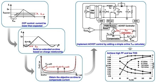
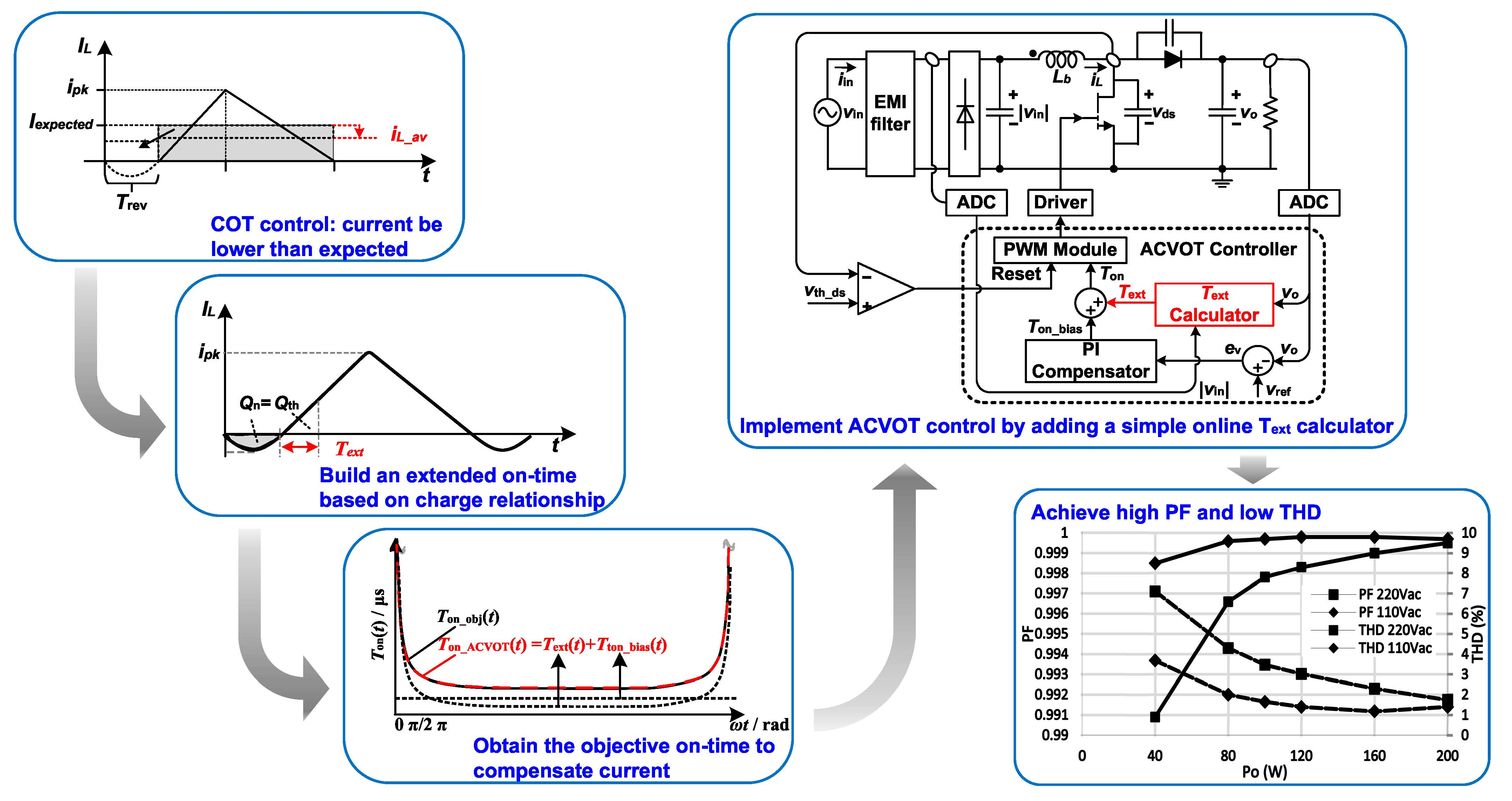
2. Proposal of ACVOT Control

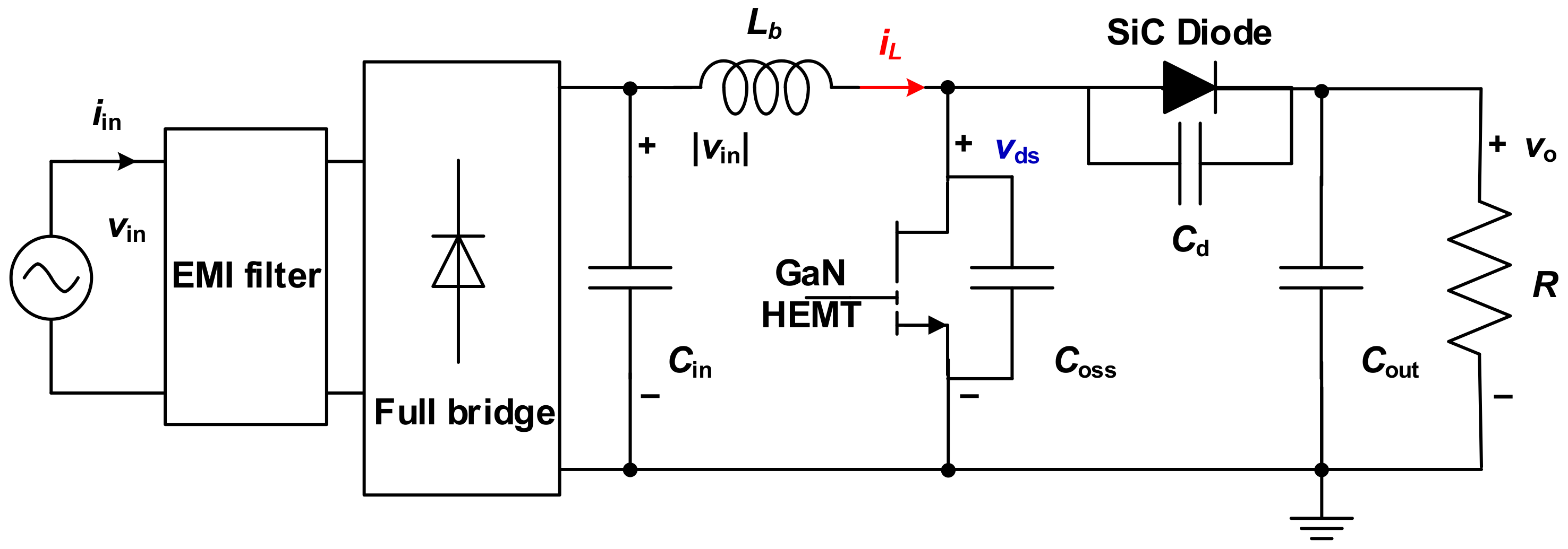
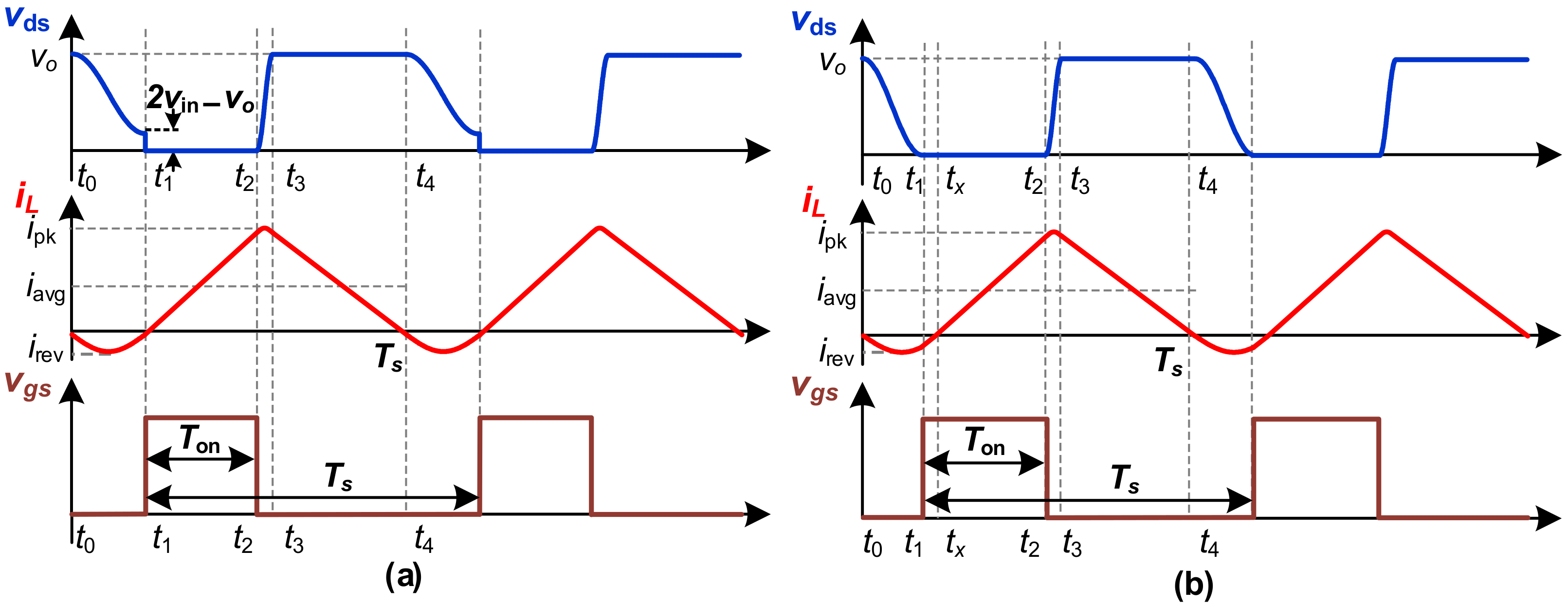
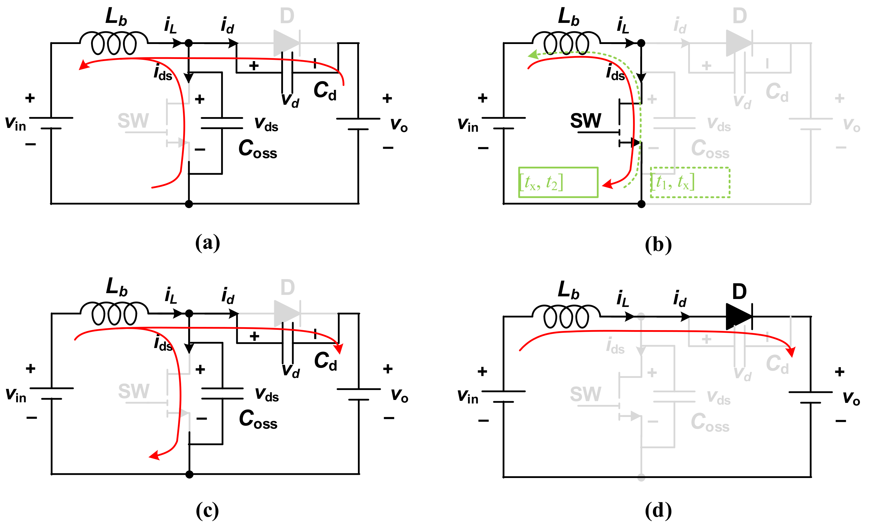
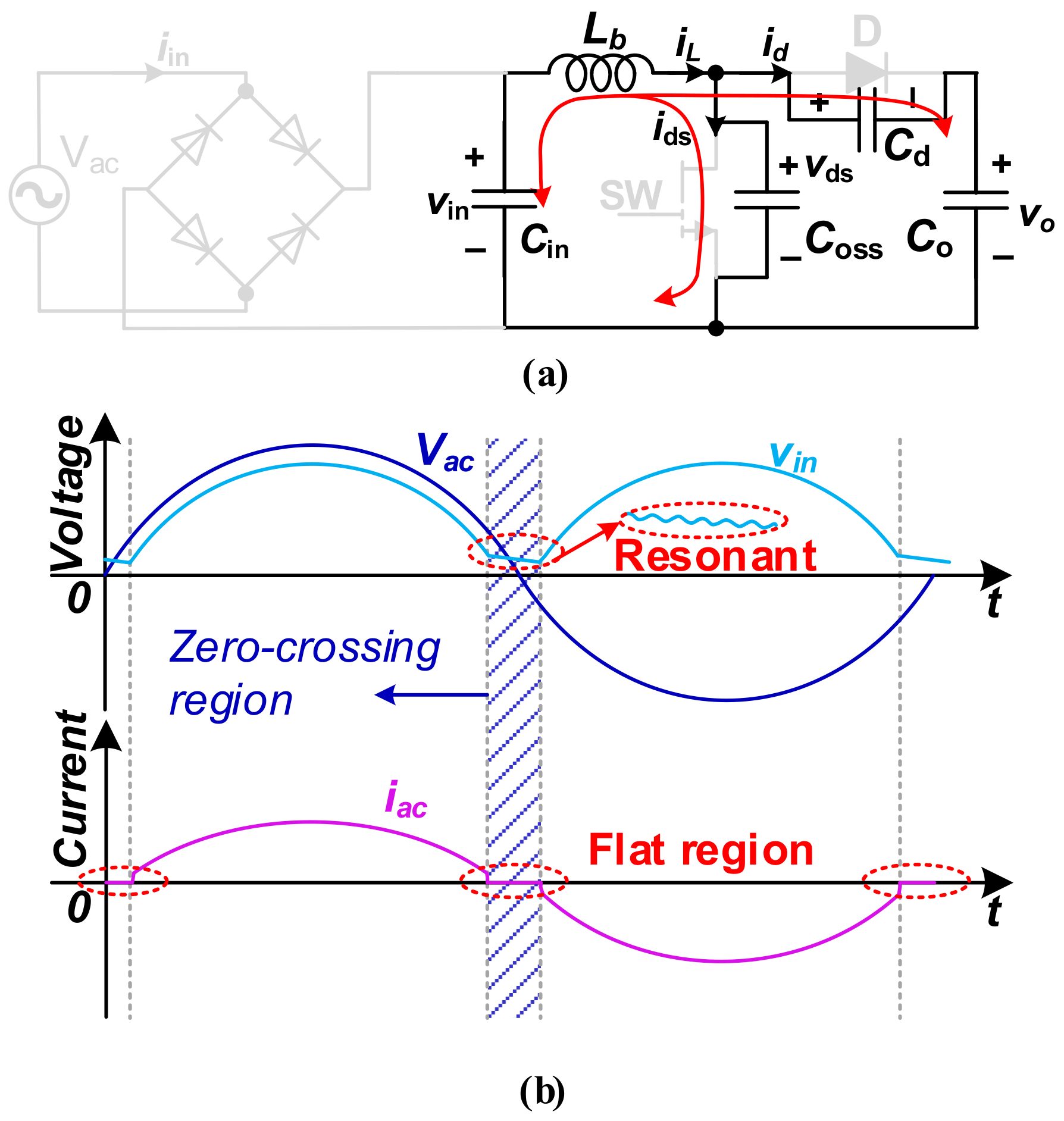
2.1. A General Analysis of CRM Boost PFC

The basic topology of a typical boost PFC converter is displayed in Figure 1, including the elements generally required, such as the EMI filter and the rectifier bridge. The GaN high-electron-mobility transistor (HEMT) and the SiC diode are used in this paper. The output junction capacitance Coss of the GaN HEMT and the parallel capacitance Cd of the SiC diode are presented.
The vs. and ZVS are vital approaches for the CRM boost converter to improve the overall operation efficiency. The key waveforms of the converter when VS/ZVS is achieved are given in Figure 2a,b. As is shown, the vgs turns high at the valley or the zero point of vds, which minimizes the switching-on loss of the power switch. In such cases, different operation stages are identified depending on the time intervals in Figure 2.
For depicting topological states, the operating circuits of each stage are included in Figure 3, where the Cin and C are treated as constant voltage sources since their voltages change slightly during one switching cycle. Unspecified parasitic parameters are ignored to highlight the most concerning part.
Firstly, the resonance process in Figure 3a,c is described by equations:
v ds = v in L b d i L d t i L = C o s s d v ds d t + C d d v d d t
where the vd = vdsvo. By solving Equation (1), the resonance stage satisfies:
v ds = A 1 cos ω r t + A 2 sin ω r t + v in i L = A 1 C eq ω r sin ω r t + A 2 C eq ω r cos ω r t
where the Ceq = Coss + Cd, ωr = sqrt (1/LbCeq), Zr = sqrt (Lb/Ceq), and A1 and A2 are the undetermined coefficients. Since the initial state of vds is vo, and the steady state of vds is vin, the criteria 2vinvo for whether the vs. or the ZVS condition is deduced. Next, different operation stages in both VS/ZVS conditions are described. The expressions for vds and iL are listed in Table 1 depending on the time intervals.
For the vs. condition (2vin > vo), there are four stages in one switching cycle.
Stage I: The reverse resonant period [t0, t1]. IL is zero at t0 instant and the initial value of vds is vo. Lb starts resonating reversely with Ceq. Stage II: The switching-on period [t1, t2]. The gate drive signal vgs stays high and iL rises linearly from zero to its peak value ipk. Stage III: The forward resonant period [t2, t3]. The power switch turn-off at t2 and Lb starts resonating forwardly with Ceq in a short period of time. Stage IV: The diode conduction period [t3, t4]. The power switch is blocked and the diode is conductive. IL decreases linearly to zero at the t4 instant.
For the ZVS condition (2vin < vo), the expression of Stage I, Stage III, and Stage IV is the same as the expression in the vs. condition. The difference in Stage II is described by the following two segmented states: Stage II-1: The switch-on period 1 [t1, tx]. The power switch becomes conductive at t1 instant and iL starts rising linearly from the reverse peak value. Stage II-2: The switch-on period 2 [tx, t2]. The power switch stays conductive and iL rises linearly from zero to its peak value ipk.
Since the equations of iL and vds are already given clearly in operation stages, the time intervals tntn−1 and the inductor charge Qn during each stage are calculated by substituting numerical boundary conditions and by using step-by-step integration. The results in Table 2 and Table 3 show a full-order model of the inductor charge.
Based on the above operation analysis, the reasons for input current distortion are now discussed.
As is known, the input current all passes through the inductor, and the average of the inductor current during the switching cycle is assumed to be iL_av = Ton(vin/Lb)/2 under COT control. Thus, with a constant Ton, the input current is in proportion to the sinusoidal input voltage in assumption. However, with the full-order inductor charge model, the iL_av is calculated as
i L _ av = Σ Q n Σ t n t n 1
where the time intervals tntn − 1 and the inductor charge Qn are given in Table 2 and Table 3. Because of the existence of the forward resonance stage and the reverse resonance stage, numerous nonlinear factors are introduced to the relation of iL_av and Ton, which distorts the input current. The reverse resonance stage is focused to reduce the distortion, since the forward resonance stage is short and has negligible influence. On the one hand, the reverse resonance decreases the charge transferred during a switching cycle. On the other hand, it increases the length of the cycle. These two points result in the iL_av being lower than expected.
Reviewing the operation of boost PFC, it is worth noting that energy is stored in the inductor Lb during the switching-on period and is transferred to the output during the diode conduction period, as shown in Figure 3b,d. However, when the energy stored in Lb is not enough to charge the Coss and discharge the Cd to let vds > vo + vdiode (vcond_diode is the conduction voltage of D), diode D cannot be turned on. The circuit enters a non-power transfer period, at which time resonance occurs, as shown in Figure 4. During this period, the energy is confined and dissipated in the tank circuit, which is composed of Cin, Lb, and Ceq.
Under COT control, the length of the switching-on period is regarded as constant. Thus, when the line voltage Vac is low near the zero-crossings, the switching-on period cannot supply sufficient energy to Lb. Non-power transfer occurs as described above. During this interval, the voltage drop rate of Cin is slow, which is determined by the relatively small loss in the resonant tank and the relatively large value of Cin. On the contrary, the line voltage decreases at a faster rate. Thus, the bridge rectifier cannot be turned on until the line voltage rises high again in the next half-line cycle. The line current iac forms a flat region during this interval, as illustrated in Figure 4b [11].
This phenomenon is called “crossover distortion”. If the energy charged during the switching-on period is described as a function of the input current, the criteria for the zero-crossing region are expressed as:
1 2 L i ac 2 1 2 C eq v o + v cond _ diode 2
Since the iac = Iac_rms·sinθPo/Vac_rms·sinθ, the θ satisfying Equation (4) is expected to increase as Po/Vac_rms decreases, which extends the zero-crossing region. Thus, serious crossover distortion occurs under COT control in case of the high input voltage with light load. Comparatively, if the VOT method is adopted to extend the switching-on period in the zero-crossing region, the distortion is expected to be significantly reduced [14].
Moreover, the input filter also affects the input current distortion. Because of the feature of the PFC, the input impedance is equivalent to a resistance when discussing the effect of the input filter. Since a capacitor Cin is commonly used, a phase leading angle ϕ1 can exist between the input current and the input voltage. It is easy to estimate ϕ1 as
i in = j 2 π f line C in + 1 R in v in tan ϕ 1 = 2 π f line C in V in _ rms 2 P o
where the Rin = Po/ V in _ rms 2 is the input equivalent resistance, fline is the line frequency, Vin_rms is the RMS value of the input voltage, and Po is the output power of the PFC converter. The current distortion caused by Cin can be reduced by introducing a phase lag into the control [23]. Since the Cin is designed small and has low effects on the input current distortion compared with the reverse resonance, Cin is ignored when considering the main method of distortion compensation for simplicity. Except for the reasons above, the errors in control, the nonlinearity, the parasitic parameters of the devices, and the voltage ripple on Cin and Cout inevitably affect the input current. However, they are negligible for the analysis.

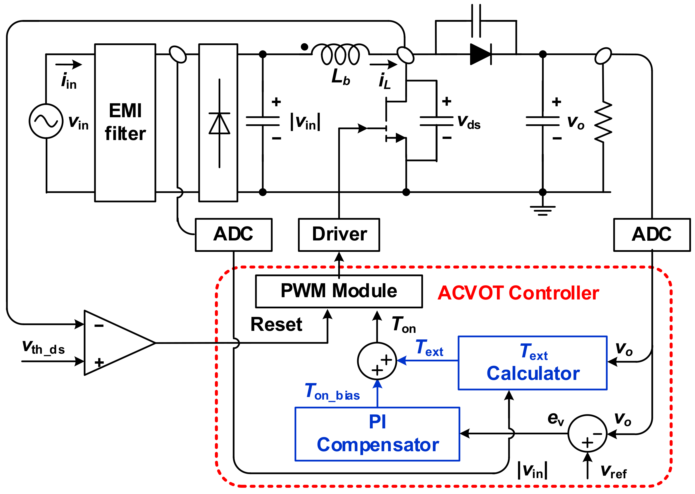
2.2. The Proposal of ACVOT Control

In order to eliminate input current distortion, the average inductor current of switching cycle should be controlled as the expected value. Assuming that the converter efficiency is η and the output power is Po, the expected input current is expressed as
i in _ expected = 2 P o η V in _ rms sin ω t
Therefore, the objective Ton_obj(t) curve that guarantees the iL_av being sinusoidal can be calculated by letting the iin_expected = iL_av, where iL_av is obtained with the full-order inductor charge model for accuracy. The Ton_obj(t) is derived as
T on _ obj ( t ) = L R 2 + L C v o ( v o 2 V in _ rms sin ( ω t ) ) ( V in _ rms sin ( ω t ) ) 2 + L C L R 2 ( v o V in _ rms sin ( ω t ) ) V out π a cos V in _ rms sin ( ω t ) v o V in _ rms sin ( ω t ) + v o V in _ rms sin ( ω t ) 2 2 v o V in _ rms sin ( ω t ) + L R + L C v o ( v o 2 V in _ rms sin ( ω t ) ) ( V in _ rms sin ( ω t ) ) 2
It is obvious that the Ton_obj(t) is too complex to directly calculate. Figure 5a shows the calculated Ton_obj(t) curve with certain circuit parameters: Po = 200 W, Vin_rms = 220 V, vo = 400 V, Lb = 200μH, Ceq = 120 pF, η = 100%, and fline = 50 Hz. It is noticed that the Ton_obj(t) curve can be treated as its shape part is superimposed on a fundamental part.
To simplify the calculation of Ton_obj(t), these two parts are considered to be acquired separately. Since the bias part is linear, utilizing feedback adjustment is suitable to avoid calculation. In addition, if the bias is adjusted by feedback, the shape curve is allowed to shift up and down as long as its shape is correct. This means that it is possible to simply obtain the shape curve using an over-compensation algorithm.
The generation of objective on-time under ACVOT control is divided into two parts accordingly. As shown in Figure 5b and Figure 6, the ACVOT controller obtains an extended on-time Text with correct curve shape using a real-time calculator while obtaining a bias on-time curve with correct amplitude using the PI compensator in each half-line cycle. The combination of Text and Ton_bias easily generate the desired on-time curve. The detailed control strategy is proposed as follows.
Since the main reason for the input current distortion is the reverse resonance in previous discussion, it is reasonable to build the Text curve based on the influence of the reverse resonance part. From the view of charge, the negative charge caused by the reverse inductor current stage needs to be compensated. Figure 7 labels the related charge during a switching cycle. The extended on-time Text is derived by building partial charge compensation in both VS/ZVS conditions.
When the vs. condition is achieved, two parts of the inductor charge are shown in Figure 7a, where the charge Qn_vs represents the level of the current distortion. To compensate Qn_vs, an extra conduction time Text is extended and Qth_vs represents the level of compensated charge by Text.
Qn_vs is Q1 in the vs. condition, as shown in Table 3. Therefore, Qn_vs is obtained by
Q n _ vs = 2 C eq v o v in ,
where t1 = Tr/2 = π sqrt(LbCeq) is the valley switching point of the resonance.
The inductor current keeps rising with the almost constant slope K = vin/Lb during the time interval [t1, t2]. Thus, Qth_vs is given by
Q th _ vs = v in T ext 2 2 L b
Let Qth_vs = Qn_vs. The extended conduction time for the vs. condition is derived as
T ext _ vs = 2 ω r v o v in v in
When the ZVS condition is achieved, two parts of the inductor charge are shown in Figure 7b, where the charge Qn_zvs during [t0, tx] represents the level of the current distortion, and Qth_zvs represents the level of the compensated charge introduced by Text.
Like with the vs. condition, Qn_zvs is the sum of Q1 and Q21 of the ZVS column in Table 3. Q1 is obtained first in Table 2, which is expressed as
Q 1 = v o C eq .
To derive Q21, the peak value of the reverse inductor current is given as i L ( t 1 ) = v o 2 2 v o v in / Z r according to the expression of iL(t) in Table 1, where t1 is derived by setting vds(t1) = 0 in expression of vds(t) in Stage I, and the time interval txt1 is given in Table 2 by setting iL(tx) = 0 in expression of iL(t) in Stage II-1. With the initial condition and the integration time, Q21 is calculated as
Q 21 = C eq v o 2 2 v o v in 2 v in
With Q1 and Q21, Qn_zvs is obtained. Thus, Qn_zvs and Qth_zvs are briefly expressed as
Q n _ zvs = C eq v o 2 2 v in Q th _ zvs = v in T ext t x t 1 2 2 L b
Let Qth_zvs = Qn_zvs. The extended conduction time for the ZVS condition is derived as
T ext _ ZVS = v o ω r v in 1 2 v in v o + v o ω r v in
The charge compensation relation Qth_vs = Qn_vs/Qth_zvs = Qn_zvs generates the required Text(t) of each cycle in both VS/ZVS conditions. Therefore, the final form of the extended on-time is established as
T ext = 2 ω r v o v in v in , v in > 0.5 v o VS v o ω r v in 1 2 v in v o + v o ω r v in , v in < 0.5 v o ZVS
Then, the initial bias on-time is estimated as
T on _ bias t = 2 L b v in t i in _ expected t
Finally, the complete on-time form of ACVOT control is expressed as
T on _ ACVOT t = T on _ bias t + T ext t
In order to obtain a good compensation effect, the Ton_ACVOT(t) curve should accord with the Ton_obj(t) curve. After adjusting the Ton_bias(t), the Ton_ACVOT(t) curve under the ACVOT control is plotted in Figure 5b with the same circuit parameters. It is obvious that the on-time curve under the proposed control and the Ton_obj(t) curve have good consistency. Further research about the ACVOT control is given in the following section.

3. Simulations and Details of the ACVOT Control

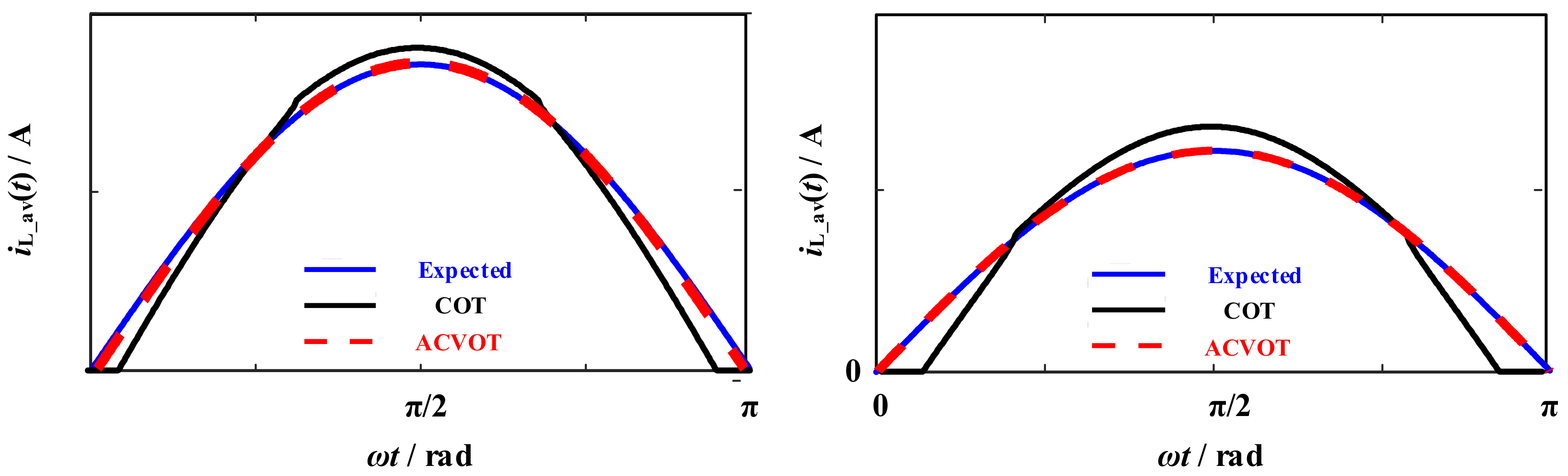
3.1. Mathematical Simulations for the ACVOT Control

In order to research the compensation effectiveness of the proposed control intuitively, close-loop mathematical simulations are applied based on the following steps:
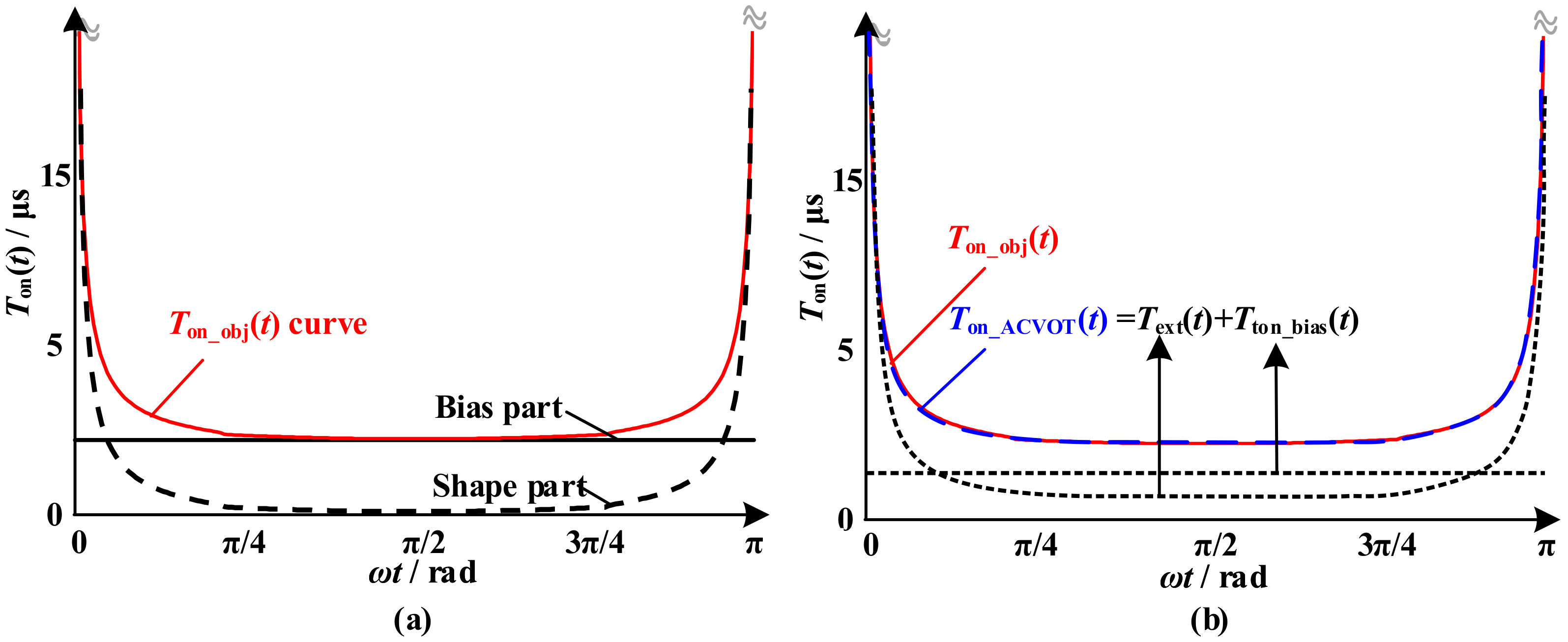
  • Under arbitrary Po and Vin_rms, the reference inductor current is given by Equation (6), the bias conduction time is given by Equation (16), and the extended on-time is determined by Equation (15). Then, the on-time Ton_ACVOT(t) curve is calculated by Equation (17).
  • With the Ton_ACVOT(t), the average inductor current curve is estimated by Equation (3). Further, the input power Pin_cal is calculated by integration in each half-line cycle. Since the feedback loop keeps adjusting the amplitude of the expected input current Iin_exp to match the output power, an adjusting process is applied as follows: when Pin_calPo > 0, the loop shifts Iin_exp downward. When Pin_calPo < 0, the loop shifts Iin_exp upward. Thus, the Pin_cal can be regulated to match the Po. After several iterations, the stable state of the closed-loop ACVOT controller is obtained.
  • The above two steps are repeated to obtain data in full input and load range. For comparison, the simulations about the COT control are also applied by the same steps.
The input current waveforms under the COT control and the ACVOT control are illustrated in Figure 8 with the simulated data, which has 200 W full load and the same circuit parameters as the previous section. It is observed that the input current waveform is significantly rectified using the ACVOT control.
Although the input current waveforms in the above cases show good effectiveness of the ACVOT control, it is worth considering that the working conditions of PFC are complex and the control parameters have deviations in real implementations. Further research is conducted to verify the adaptivity of ACVOT control.
To show the feasibility of the ACVOT control in a wide input and load range, quantitative analysis of current distortion is established using PF and THD calculations. For a list of stable states at different Po and Vin_rms conditions, the PF and THD values are estimated by
P F = P in V in _ rms I rms = 1 π 0 π v in t i in t d ω t V in _ rms 1 π 0 π i in 2 t d ω t THD = cos θ / P F 2 1
where θ is the angle between the vin and the fundamental component of iin. θ is equal to 1 in calculation because the input filter is ignored.
The close-loop THD mapping under ACVOT control is shown in Figure 9b. For contrast, the THD mapping under COT control is plotted in Figure 9a. It is obvious that the ACVOT control is expected to effectively reduce the current distortion in a wide input and load range.
It is important to verify the sensitivity of values of Lb and Ceq under the ACVOT control, since they have large tolerance and the Ceq varies according to the variation of the drain–source voltage. Thus, the simulation is carried out with ±20% tolerance of the values of Lb and Ceq. The simulated PF and THD surfaces against different Lb and Ceq values with full load are shown in Figure 10 and Figure 11. Limited by the article length, surfaces under different load conditions are not plotted but they have the same trend as Figure 10 and Figure 11. It is observed that the ACVOT control slightly changes the THD and PF values under the variation range of Lb and Ceq. Moreover, better THD and PF occurs when the negative Lb and positive Ceq variations are achieved. Thus, a small Lb value and a large Ceq value are recommended to set.

3.2. Implementation Problems of ACVOT Control

Figure 6 illustrates the implementation of the proposed control, which is further discussed here.
In practical terms, the proposed control can be implemented based on a prior COT system, which mainly includes an input/output sampler, a voltage loop compensator, a PWM generator, and a valley/zero-voltage switching optimizer. In general, only an additional Text calculator is required for the proposed solution. This calculator uses the input, the output, the inductor value Lb, and the parasitic capacitance value Ceq to calculate Equation (15). Furthermore, its output is added to the output of voltage compensator, as shown in Figure 6, which is similar to a current loop compensator. The calculator consumed resources are discussed in Section 3.3. Without other required operations, the proposed solution is easy to implement. Moreover, the calculation of Text is feasible for common digital processors and chips. The proposed solution is flexible to be realized by DSP or ARM.
Furthermore, considering the practical problems of the ACVOT control, some essential details require explanation.
Firstly, input voltage sampling before the rectifier bridge is recommended, since it avoids the residual voltage of Cin near the input zero-crossing point. Otherwise, the additional phase lock model is required to obtain the sinusoidal input voltage.
Secondly, it is important to realize the detection of the VS/ZVS point. As illustrated in Figure 6, voltage-based detection is adopted in this paper. If the vds_th = max(2vinvo, 0) is set, the RESET signal flips at the valley or zero-voltage point of vds according to the operation condition. In addition, a small offset is added to vds_th to ensure the comparator be trigged ahead of time, which also compensates for the detection delay.
Thirdly, the consideration of Ceq is simple under ACVOT control. Although the variations of Ceq are difficult to solve under different drain–source voltage curves and the piecewise equivalent method in [24] is more precise, using a constant Ceq is enough under ACVOT control in most implementations because Ceq is not sensitive under ACVOT control.
In addition, although the analytical solution of Text(t) is continuous at the boundary of VS/ZVS conditions, it is better to make minor boundary adjustments to ensure a smooth Text(t) curve when boundary error exists in implementation.

3.3. Features of ACVOT Control

The ACVOT control has the advantage of achieving both high performance and easy implementation. Related features are summarized as the following aspects:
  • Only a simple and fixed calculation is required to realize the compensation within the universal ac input and entire load range. There is no need to detect the maximum value of input voltage or calculate the phase of input voltage, and any pre-calculation procedure is avoided for designers.
  • The longest chain length of total calculation is six and they are basic operations except for one square root operation. To evaluate the resource consumption, an FPGA controller (EP4CE22F17C8N with ALTFP calculation IP cores) is used, the time and space consumption is reflected by the required clock-cycles, and the LUTs/registers resource is used. Table 4 compares the computing consumption between the ACVOT control and the control in [22], since [22] has the lowest operations consumption among the referenced digital methods that are not LUT-based (explained in Appendix A). As shown in Table 4, the ACVOT control consumes 54%/43% less LUTs/registers resources than the previous control.
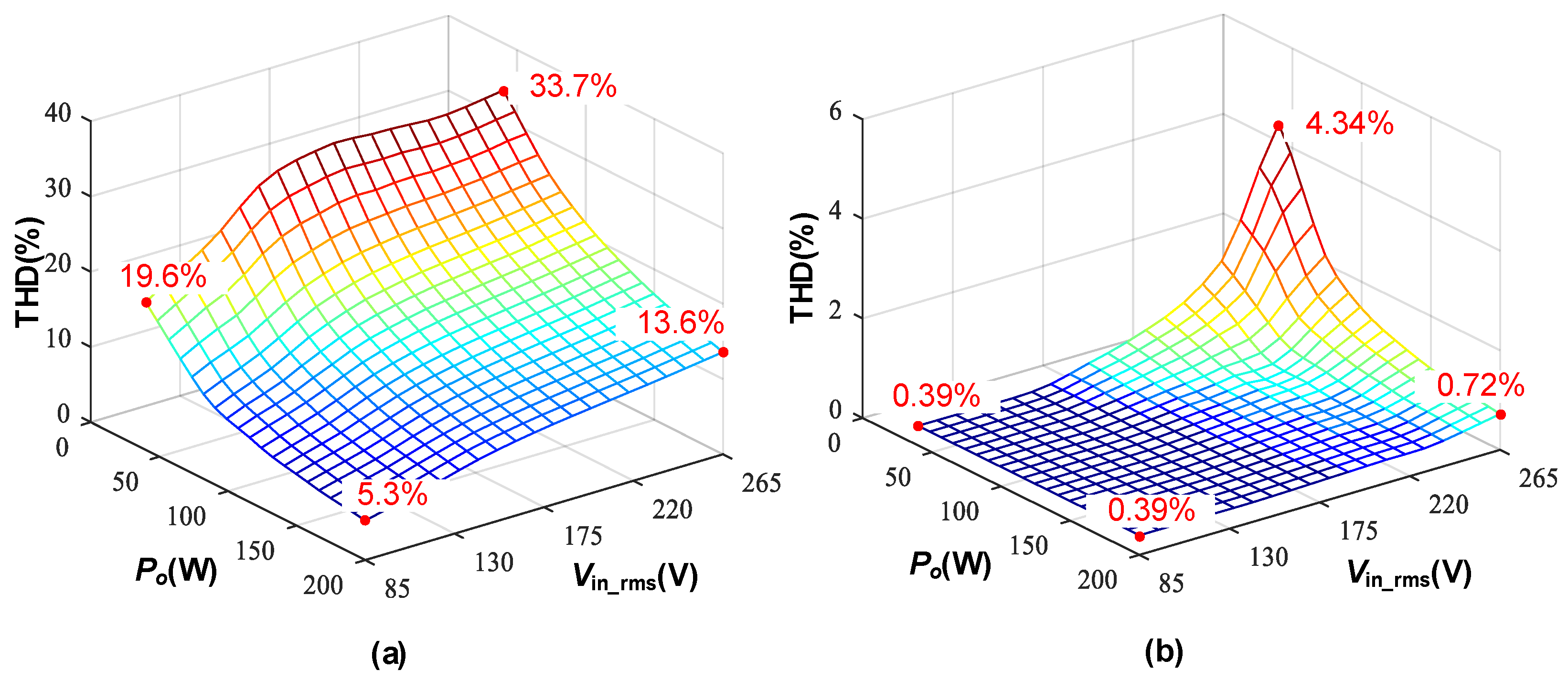
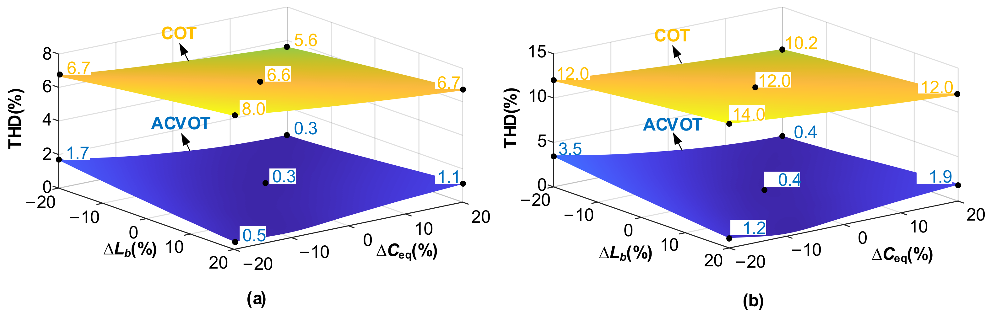
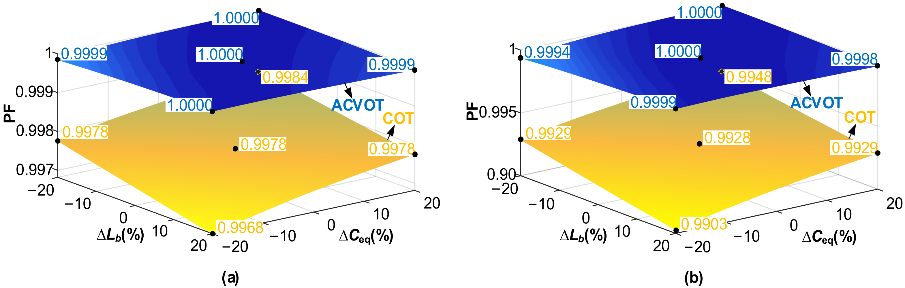
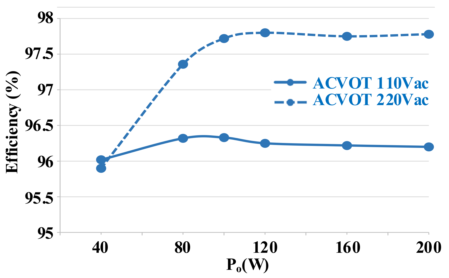
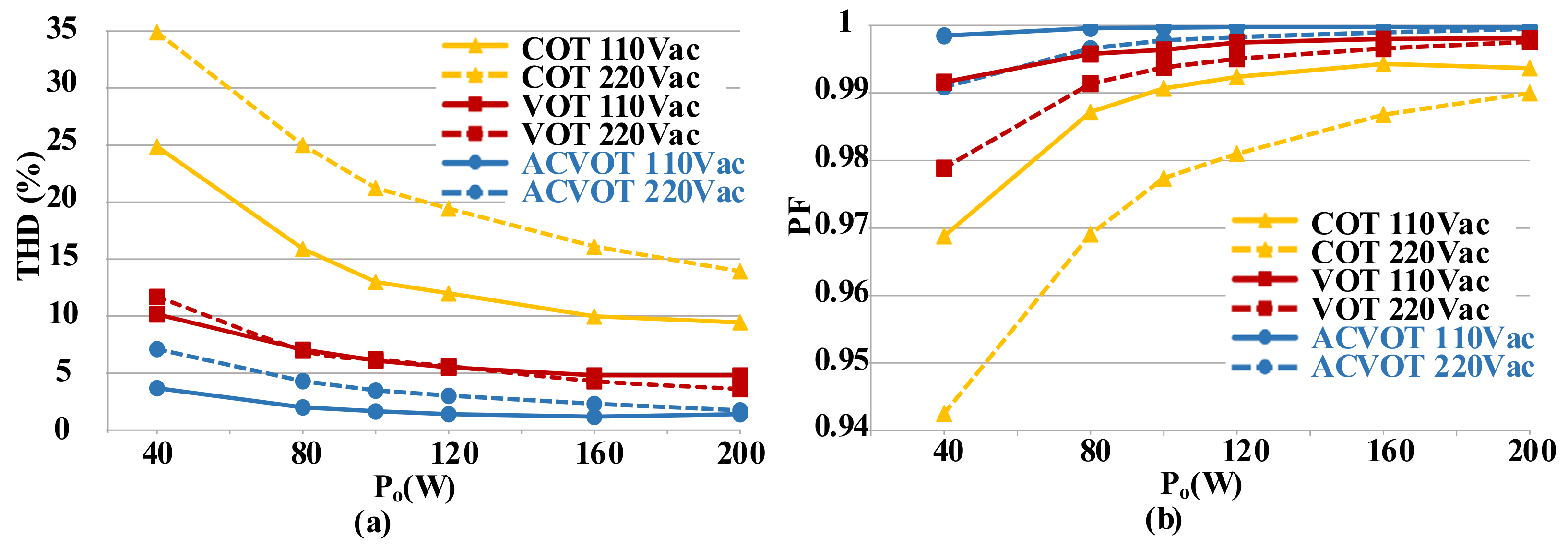
  • Moreover, the input current distortion can be significantly reduced. According to Fourier analysis, the total harmonic component is less than 1% of the fundamental waveform at the condition in Figure 8. The fault tolerance of Lb and Ceq is sufficient, which guarantees the robustness of the ACVOT control. The experiments in the next section further verify the performance of the ACVOT control. In general, it is a real-time method with minimal cost but remarkable performance among the VOT controls.

4. Experimental Results and Discussions

A 200 W boost PFC prototype is used to verify the effectiveness of the ACVOT control, which has main specifications in Table 5. Figure 12 gives a photograph of the experimental boost PFC prototype. The control implementation diagram is the same as Figure 6. The core material of the inductor Lb is PQ20/16-3F36 from FERROXCUBE. The Ceq is derived by the Coss and Cd capacitance given in datasheets, based on a time-related equivalent model.
The board is modularity-based. The control module uses an FPGA chip Cyclone IV EP4CE22F17C8N from INTEL. The ADC modules use LTC2314-14 chips from TI and two ADC modules are used in the prototype. A 220nF CBB capacitor is adopted for filtering near the input. An 180 μF electrolytic capacitor is adopted near the output. The high-speed comparator TLV3501 is used to generate the RESET signal.
The experimental waveforms of vin, iin, and iL at 110/220 Vac with 20%/100% load are shown in Figure 13 and Figure 14 (measured with oscilloscope MDO3054 and current probe CPA300A). It is observed that there is serious input current distortion near the zero-crossing point of the input voltage under the COT control, while the distortion is obviously reduced under the ACVOT control.
It is noteworthy that the maximum value of Ton_ACVOT(t) is limited to 25 μs near the zero-crossing point for safety in experiments. Thus, the experiment results are slightly limited at the light load, at which time Cin also has a bigger effect. However, the light load condition is not necessary for PFC function, and the experimental results are acceptable and convincing for proving the improvement in the input current distortion.
Figure 15 gives the measured efficiency of the boost PFC prototype, and Figure 16a,b give the PF and THD charts at 110 Vac/220 Vac input with full load under the ACVOT control and the COT control (measured using the high-precision-power analyzer PA5000H). It is observed that the THD and PF are improved greatly within the entire load range at different AC input voltages under the proposed control. From Figure 16a, the input current THD is reduced to 1.4% at 110 Vac input with full load and 1.7% at 220 Vac input with full load.
Table 6 shows the comparison between the ACVOT control strategy and the previous VOT control strategies. Since [18] had relatively low THD data in the table, we also repeated the VOT control process in [18] at our board and showed the results in Figure 16a,b. Some of the differences shown between the data in Figure 16a and Table 6 are due to different prototypes used. In comparison, the proposed method achieves lower THD than other real-time control methods and achieves low THD levels close to reference [18]. It is noticed that [18] is based on a look-up table method. The difference between LUT implementation and real-time implementation can be explained. Method in [18] is roughly realized by:
  • Establishing a MATLAB file to estimate the average inductance current iL_av (according to all fifteen equations in Table 1 and Table 2);
  • Building an iterative model to acquire a table with right on-time values, which finally fits specific sinusoidal iL_av curve;
  • Converting the table into a suitable storage file (satisfy different controllers of small power converter);
  • Adding storage units and accessing logic to the controller;
  • Adding accurate input phase detection to help table look-up.
Table 6. Comparison of the different control strategies.
ControlsACVOT[15][18][20][22][25]
Input line voltage90–240 Vac90–240 Vac90–264 VacN/A90–230 VacN/A
Output voltage400 V400 V400 V400 V380 V400 V
Rated power200 W200 W160 W30 W200 W100 W
Efficiency (max)97.8%N/A98.35%91.6%97.35%N/A
Input current THD (at rated power)1.4%
at 110 Vac
3.9%
at 110 Vac
0.97%
at 110 Vac
Lack of data4.3%
at 90 Vac
3.74%
at 110 Vac
1.7%
at 220 Vac
Lack of data2.9%
at 220 Vac
5.6%
at 220 Vac
9.8%
at 230 Vac
5.5%
at 220 Vac
Control methodCRM, digital
Real-time
CRM/DCM, analogCRM, digital
LUT-based
CRM, digital
Real-time
CRM, digital
Real-time
CRM, digital
Real-time
The method in this article is realized by:
  • Adding a several lines of the computing code (according to Equations (15) and (17)) in the prior control program).
As noted above, the easy implementation of the proposed method should be considered as a significant advantage for engineering. In summary, the ACVOT control is remarkable for its performance and easy implementation.

5. Conclusions

This paper proposes an adaptive charge-compensation-based control strategy for CRM boost PFC. The control strategy is established using the partial charge compensation algorithm and the feedback loop. A bias on-time is generated using the feedback loop. Furthermore, an extended on-time is calculated online using an algorithm to compensate the charge during the reverse inductor current stage. The above two times are added up to obtain the objective on-time, which avoids the need for numerous computing resources to directly obtain the accurate on-time. The proposed strategy improves the THD and reduces the LUT/register resources by 54%/43% in FPGA realization. Good adaptivity and robustness are shown in simulations and experiments. The input current THD is only 1.4% at the 110 Vac input with the full load and 1.7% at the 220 Vac input with the full load, supported by the 200 W prototype.

Author Contributions

Conceptualization and methodology, D.Z. and W.W.; resources, F.Z.; software and validation, N.L.; writing—review and editing, X.L.; supervision and project administration, J.Y. All authors have read and agreed to the published version of the manuscript.

Funding

This was funded by the National Natural Science Foundation of China (under grant 62074067).

Data Availability Statement

The datasets used and/or analyzed during the current study are available from the corresponding author upon reasonable request.

Acknowledgments

This work is supported by the Hubei Jiufengshan Laboratory and the Huazhong University of Science and Technology.

Conflicts of Interest

The authors declare that they have no conflict of interest.

Appendix A

To explain why [22] has the lowest operations consumption among the referenced digital methods, as opposed to being LUT = based. Authors briefly list the key equations required for mentioned referenced methods in Table A1 [20,22,25], which correspond to Table 6. Moreover, Ref. [19] is excluded because it is used for totem-pole PFC, and Ref. [21] is excluded because it lacks specific calculations.
To simplify this information, symbols in the original equations are replaced by symbols with the same meaning in this paper, and complicated values which can be calculated in advance are replaced by constant symbols G1, G2, …. The readers should note the differences introduced by conversion of the expression styles.
Table A1. The key equations required for mentioned referenced methods.
ControlsEquations for the ZVS ConditionEquations for the vs. Condition
[20] M = v o v in T on = G 1 + M 1 G 2
k 1 = G 3 v in + i L t 3 G 4 v in + G 5 v o + G 6 i L t 3
k 2 = G 7 M M 1  
T s = T on + k 1 + k 2
[22] M = v in v o , M = v o v in k 1 = 1 M T on G 8 + G 9 M 2 4 T on = k 1 + G 10 M 1 2 1 M = v in v o , M = v o v in k 1 = 1 M T on G 8 + G 9 3 M + 4 M 8 T on = k 1
[25] M = v o v in k 1 = G 11 ( G 12 + M 1 sin G 12 ) T on = G 13 + G 13 2 + 4 M 1 G 13 + k 1 π 2 M 2 k 1 2 M = v o v in k 1 = G 14 G 12 + G 15 M 1 T on = G 13 + G 13 2 + 4 M 1 M k 1 2
The required basic arithmetic units can be counted using the equations with consistent form in Table A1. This table shows that the equations in [22] have relatively few required computation consumptions.

References

  1. Tayar, T.; Abramovitz, A.; Shmilovitz, D. DCM Boost PFC for High Brightness LED Driver Applications. Energies 2021, 14, 5486. [Google Scholar] [CrossRef]
  2. Castellan, S.; Buja, G.; Menis, R. Single-phase power line conditioning with unity power factor under distorted utility voltage. Int. J. Electr. Power 2020, 121, 106057. [Google Scholar] [CrossRef]
  3. Gerber, D.L.; Musavi, F.; Ghatpande, O.A.; Frank, S.M.; Poon, J.; Brown, R.E.; Feng, W. A Comprehensive Loss Model and Comparison of AC and DC Boost Converters. Energies 2021, 14, 3131. [Google Scholar] [CrossRef]
  4. Ren, X.Y.; Zhou, Y.T.; Guo, Z.H.; Wu, Y.; Zhang, Z.L.; Chen, Q.H. Simple Analog-Based Accurate Variable On-Time Control for Critical Conduction Mode Boost Power Factor Correction Converters. IEEE J. Emerg. Sel. Top. Power 2020, 8, 4025–4036. [Google Scholar] [CrossRef]
  5. Liu, B.; Wu, J.J.; Li, J.; Dai, J.Y. A novel PFC controller and selective harmonics suppression. Int. J. Electr. Power 2013, 44, 680–687. [Google Scholar] [CrossRef]
  6. Min, R.; Tong, Q.L.; Zhang, Q.; Chen, C.; Zou, X.C.; Lv, D.A. Corrective frequency compensation for parasitics in boost power converter with sensorless current mode control. Int. J. Electr. Power 2018, 96, 274–281. [Google Scholar] [CrossRef]
  7. Santos, A.; Duggan, G.P.; Young, P.; Frank, S.; Hughes, A.; Zimmerle, D. Harmonic cancellation within AC low voltage distribution for a realistic office environment. Int. J. Electr. Power 2022, 134, 107325. [Google Scholar] [CrossRef]
  8. Marxgut, C.; Krismer, F.; Bortis, D.; Kolar, J.W. Ultraflat Interleaved Triangular Current Mode (TCM) Single-Phase PFC Rectifier. IEEE Trans. Power Electron. 2014, 29, 873–882. [Google Scholar] [CrossRef]
  9. Datasheet of L6562AT Transition-Mode PFC Controller. Available online: https://www.st.com/resource/en/datasheet/l6562at.pdf (accessed on 26 April 2022).
  10. Datasheet of UCC28063 Natural Interleaving™ Transition-Mode PFC Controller. Available online: https://www.ti.com/lit/gpn/UCC28063A (accessed on 26 April 2022).
  11. Su, Y.; Ni, C.; Chen, C.; Chen, Y.; Tsai, J.; Chen, K. Boundary Conduction Mode Controlled Power Factor Corrector With Line Voltage Recovery and Total Harmonic Distortion Improvement Techniques. IEEE Trans. Ind. Electron. 2014, 61, 3220–3231. [Google Scholar] [CrossRef]
  12. Tsai, J.C.; Chen, C.L.; Chen, Y.T.; Ni, C.L.; Chen, C.Y.; Chen, K.H.; Chen, C.J.; Pan, H.L. Perturbation on-Time (POT) Control and Inhibit Time Control (ITC) in Suppression of THD of Power Factor Correction (PFC) Design. In Proceedings of the 2011 IEEE Custom Integrated Circuits Conference (CICC), San Jose, CA, USA, 19–21 September 2011; pp. 1–4. [Google Scholar]
  13. Tang, S.H.; Chen, D.; Huang, C.S.; Liu, C.Y.; Liu, K.H. A new on-time adjustment scheme for the reduction of input current distortion of critical-mode power factor correction boost converters. In Proceedings of the 2010 International Power Electronics Conference—ECCE ASIA, Sapporo, Japan, 21–24 June 2010; pp. 1717–1724. [Google Scholar]
  14. Guo, Z.; Ren, X.; Wu, Y.; Zhang, Z.; Chen, Q. A novel simplified variable on-time method for CRM boost PFC converter. In Proceedings of the 2017 IEEE Applied Power Electronics Conference and Exposition (APEC), Tampa, FL, USA, 26–30 March 2017; pp. 1778–1784. [Google Scholar]
  15. Chen, Y.; Chen, Y. Line Current Distortion Compensation for DCM/CRM Boost PFC Converters. IEEE Trans. Power Electron. 2016, 31, 2026–2038. [Google Scholar] [CrossRef]
  16. Marxgut, C.; Biela, J.; Kolar, J.W. Interleaved Triangular Current Mode (TCM) resonant transition, single phase PFC rectifier with high efficiency and high power density. In Proceedings of the 2010 International Power Electronics Conference—ECCE ASIA, Sapporo, Japan, 21–24 June 2010; pp. 1725–1732. [Google Scholar]
  17. Wu, Y.; Ren, X.; Li, K.; Zhang, Z.; Chen, Q. An Accurate Variable On-time Control for 400Hz CRM Boost PFC Converters. In Proceedings of the 2019 IEEE Applied Power Electronics Conference and Exposition (APEC), Anaheim, CA, USA, 17–21 March 2019; pp. 734–738. [Google Scholar]
  18. Ren, X.; Guo, Z.; Wu, Y.; Zhang, Z.; Chen, Q. Adaptive LUT-Based Variable On-Time Control for CRM Boost PFC Converters. IEEE Trans. Power Electron. 2018, 33, 8123–8136. [Google Scholar] [CrossRef]
  19. Liu, Z.; Huang, Z.; Lee, F.C.; Li, Q.; Yang, Y. Operation analysis of digital control based MHz totem-pole PFC with GaN device. In Proceedings of the 2015 IEEE 3rd Workshop on Wide Bandgap Power Devices and Applications (WiPDA), Blacksburg, VA, USA, 2–4 November 2015; pp. 281–286. [Google Scholar]
  20. Wang, J.; Eto, H.; Kurokawa, F. Optimal Zero-Voltage-Switching Method and Variable ON-Time Control for Predictive Boundary Conduction Mode Boost PFC Converter. IEEE Trans. Ind. Appl. 2020, 56, 527–540. [Google Scholar] [CrossRef]
  21. Bianco, A.; Adragna, C.; Scappatura, G. Enhanced constant-on-time control for DCM/CCM boundary boost PFC pre-regulators: Implementation and performance evaluation. In Proceedings of the 2014 IEEE Applied Power Electronics Conference and Exposition—APEC 2014, Fort Worth, TX, USA, 16–20 March 2014; pp. 69–75. [Google Scholar]
  22. Kim, J.; Youn, H.; Moon, G. A Digitally Controlled Critical Mode Boost Power Factor Corrector With Optimized Additional On Time and Reduced Circulating Losses. IEEE Trans. Power Electron. 2015, 30, 3447–3456. [Google Scholar] [CrossRef]
  23. Louganski, K.P.; Lai, J. Active Compensation of the Input Filter Capacitor Current in Single-Phase PFC Boost Converters. In Proceedings of the 2006 IEEE Workshops on Computers in Power Electronics, Troy, NY, USA, 16–19 July 2006; pp. 282–288. [Google Scholar]
  24. Lyu, D.; Shi, G.; Min, R.; Tong, Q.; Zhang, Q.; Li, L.; Shen, G. Extended Off-Time Control for CRM Boost Converter Based on Piecewise Equivalent Capacitance Model. IEEE Access 2020, 8, 155891–155901. [Google Scholar] [CrossRef]
  25. Kim, J.-W.; Yi, J.-H.; Cho, B.-H. Enhanced Variable On-time Control of Critical Conduction Mode Boost Power Factor Correction Converters. J. Power Electron. 2014, 14, 890–898. [Google Scholar] [CrossRef] [Green Version]
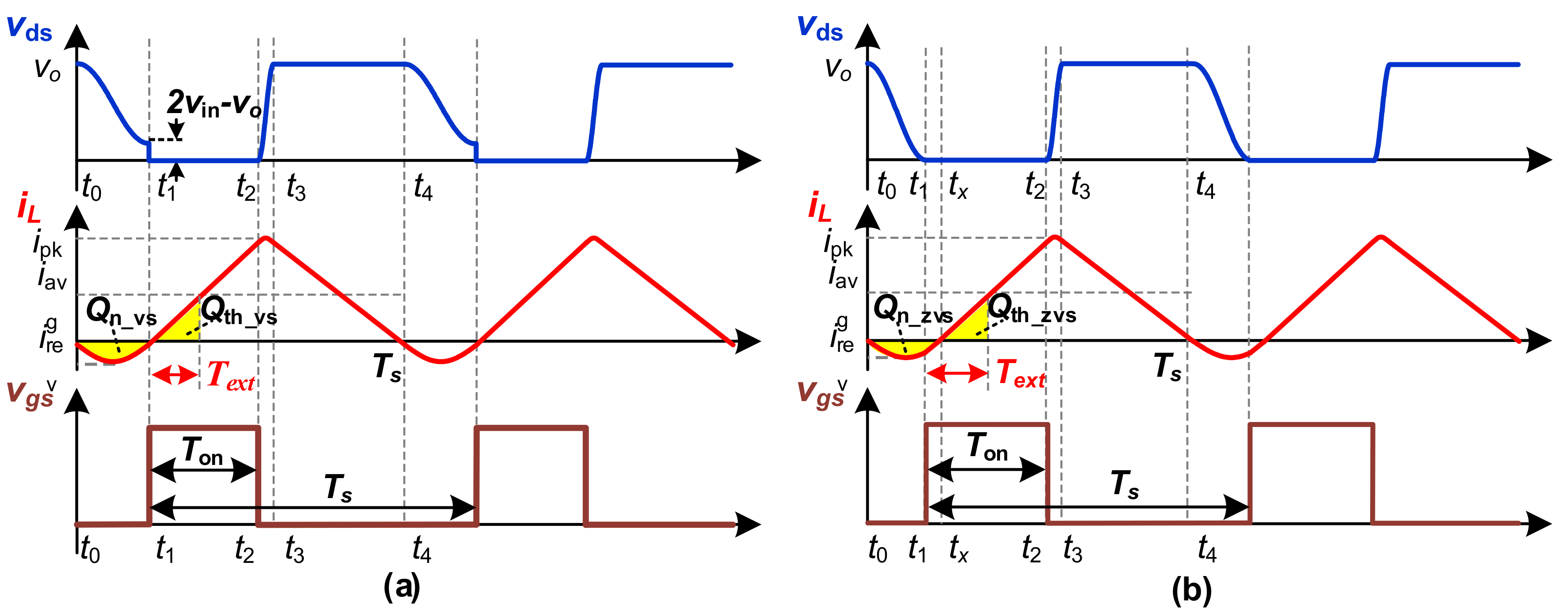
Figure 1. Boost PFC converter circuit with the GaN high-electron-mobility transistor (HEMT) and the SiC diode.
Energies 15 04021 g001
Figure 2. Key waveforms of CRM operations: (a) the vs. condition (2vin > vo); (b) the ZVS condition (2vin < vo).
Energies 15 04021 g002
Figure 3. Operating circuits: (a) the reverse resonant period, i.e., [t0, t1]; (b) the switching-on period, i.e., [t1, t2]; (c) the forward resonant period, i.e., [t2, t3]; (d) the diode conduction period, i.e., [t3, t4].
Energies 15 04021 g003
Figure 4. Typical operating circuit and waveforms in the crossover distortion phenomenon: (a) operating circuit during the non-power transfer period; (b) line voltage and current waveforms of the crossover distortion phenomenon.
Energies 15 04021 g004
Figure 5. Ton(t) curve with certain circuit parameters: (a) objective on-time curve, (b) calculated on-time curve under ACVOT control.
Energies 15 04021 g005
Figure 6. Implementation of the proposed control.
Energies 15 04021 g006
Figure 7. Diagram of the key inductor charge and the extended time of the ACVOT control: (a) the vs. condition (2vin > vo); the (b) ZVS condition (2vin < vo).
Energies 15 04021 g007
Figure 8. The simulated input current waveforms with full load under the COT control and the ACVOT control.
Energies 15 04021 g008
Figure 9. The close-loop THD mappings: (a) the COT control; (b) the ACVOT control.
Energies 15 04021 g009
Figure 10. The THD surfaces with Lb and Ceq deviations: (a) 110 Vac; (b) 220 Vac.
Energies 15 04021 g010
Figure 11. The PF surfaces with Lb and Ceq deviations: (a) 110 Vac; (b) 220 Vac.
Energies 15 04021 g011
Figure 12. The experimental boost PFC prototype.
Energies 15 04021 g012
Figure 13. Waveforms at 110 Vac with 20%/100% load: (a) under the COT control; (b) under the ACVOT control.
Energies 15 04021 g013
Figure 14. Waveforms at 220 Vac with 20%/100% load: (a) under the COT control; (b) under the ACVOT control.
Energies 15 04021 g014
Figure 15. Measured efficiency of the prototype under the ACVOT control.
Energies 15 04021 g015
Figure 16. Measured input current PF and THD comparison: (a) THD; (b) PF.
Energies 15 04021 g016
Table 1. Expressions for vds and iL depending on the time intervals.
Time Intervalsvds(t)iL(t)
[t0, t1] v in v in v o cos ω r t t 0 v in v o Z r sin ω r t t 0
[t1, t2]0 For   VS , v in L b t t 1
For   ZVS ,   t 1 , t x i L t 1 + v in L b t t 1 t x , t 2 v i n L b t t X
[t2, t3] v in v in cos ω r t t 2 + Z r i L t 2 sin ω r t t 2 i L t 2 cos ω r t t 2 + v in Z r sin ω r t t 2
[t3, t4] v o i L ( t 3 ) v o v in L b ( t t 3 )
Table 2. Lists of the time intervals during the switching cycle.
StageThe ZVS ConditionThe VS Condition
I t 1 t 0 = 1 ω r π arccos v in v o v in t 1 t 0 = π ω r
II-1 t x t 1 = 1 ω r v in v o 2 2 v o v in t 2 t 1 = T on
II-2 t 2 t x = T on 1 ω r v in v o 2 2 v o v in
III t 3 t 2 = 1 ω r arcsin v in v in 2 + Z r i L t 2 2 + arcsin v o v in v in 2 + Z r i L t 2 2
IV t 4 t 3 = L b v o v in i L t 3
Table 3. Lists of the inductor charges during the cycle.
StageThe ZVS ConditionThe VS Condition
I Q 1 = C eq v o Q 1 = 2 C eq v o v in
II-1 Q 21 = C eq v o 2 v in v o 2 v in Q 2 = v in 2 L b T on 2
II-2 Q 22 = v in 2 L b T on 1 ω r v in v o 2 2 v o v in 2
III Q 3 = C eq v o Q 3 = C eq v o
IV Q 4 = v in 2 2 L v o v in T on v o v o v in ω r v in 2 v o v o 2 v in ω r 2 v in 2
Table 4. Computing consumption of the proposed method and the method in [22].
Proposed[22]
VSZVSVSZVS
Counts of SQRT1112
Counts of DIV1222
Counts of MUL1357
Counts of ADD1246
Clock-cycles6270
LUTs/Registers1126/55122443/9738
Table 5. The main specifications of the prototype.
ItemsValuesItemsValues
Input voltage90–245 VacLb287 μH
Output voltage400 VdcCoss142 pF
Rated power200 WCd38 pF
Power switchGS66508TCeq (Coss + Cd)180 pF
Power diodeSTPSC8H065Cin220 nF
Rectifier bridgeGBU6JCout180 μF
Publisher’s Note: MDPI stays neutral with regard to jurisdictional claims in published maps and institutional affiliations.

