1. Introduction
Electric vehicles (EVs) are promising due to their eco-friendly features such as saving fossil fuels and reducing emissions [
1]. When it comes to EV charging, wireless power transfer (WPT) is an attractive method thanks to its incredible merits. For example, WPT can avoid tangled wires and become integrated with the parking bay, thereby improving convenience [
2]. There is no need to plug-in or unplug operations. This means reduced abrasion and an extension of the service life of applications [
3]. Compared with traditional conductive EV charging, WPT can avoid electric shock or arc [
4,
5]. Fortunately, these advantages can be further enlarged by dynamic wireless power transfer (DWPT) because it can charge EVs, either while running or parked [
6,
7]. Not only can the driving range be extended, but a smaller battery pack can be realized as well [
8,
9].
In general, there are two typical DWPT structures, i.e., long-track-loop structure and multiple-individual-transmitter structure [
10]. The advantage of the long-track-loop type is its simple structure. Nevertheless, drawbacks such as low coupling and low efficiency hinder its development. The high level of exposure to electromagnetic field (EMF) is another problem, because its entire transmitter is constantly energized no matter where the receiver is. Accordingly, the multiple-individual-transmitter structure is proposed to resolve these problems. It is also called segmented DWPT because multiple-segmented transmitters are placed one by one to build a charging route. One fundamental function is that transmitters can be switched on or off according to the position of the receiver. Therefore, higher efficiency and low level of exposure to EMF can be achieved compared with the long-track loop structure [
11,
12,
13,
14].
Impressively, Li et al. proposed a segmented DWPT system to address electric vehicle range anxiety and the on-board cost [
15]. It reduces the unwanted couplings between adjacent transmitters and ensures a stable mutual inductance between transmitters and the receiver. The coupling structure is made up of LITZ-wire coils and ferrite plates. A related winding technique to reduce the conductor loss is reported to reduce the loss further [
16]. The technique is used to provide a winding method for any shape of the ferrite core. The method for turn pitch and stranded winding structure can be designed using this method and further reduce the loss. Most importantly, the load-independent output is another practical concern for charging EVs. The magnetic coupler in [
15] can achieve the constant output directly by passive components without using any sophisticated control method [
17]. This paper draws upon these experiences with this coupler, given that it dramatically simplifies the entire system.
Nevertheless, previous segmented DWPT studies [
8,
14,
15] mainly focus on using one inverter to drive several transmitters. In terms of high-power applications, using one inverter to drive is very difficult because of the high current or voltage stress on semiconductor components. Additionally, the switching sequence still needs clarifying. Hence, this paper presents one improved and integrated design to resolve the problems mentioned above. The key contributions are summarized as follows:
- (1)
A modified switching sequence: The switching means turning on/off coils. The proposed switching sequence seeks to establish a balance between minimizing energized transmitters and reducing the magnetic coupling variation. Only three consecutive transmitters are energized according to the receiver position, which can ensure stable power transmission for EVs. In this paper, a combination of a Q-shaped coil, DD shaped coil and Q-shaped coil (QDDQ) is used as an elementary energized group. Specifically, QDDQ refers to a group of three consecutive coils, i.e., a Q-shaped coil, a DD-shaped coil, and a Q-shaped coil again;
- (2)
The integrated design for high-power transfer: The magnetic coupler is refined for high-power transfer and stable operation through the ANSYS Maxwell. The transmitter (TX) and receiver (RX) coils are all designed as 500 mm × 500 mm, which ensures enough magnetic coupling to avoid the power-null phenomenon. Compared with using only one inverter, parallel inverters can reduce the current stress of semiconductor devices like MOSFET. Thus, the presented method is suitable for high-power applications.
The experimental results show that this research can make the load-independent constant voltage (CV) charging possible, which is vital to charge a typical battery because its equivalent resistance is changed during the entire charging process. Moreover, the overall dynamic wireless charging efficiency (dc-dc efficiency) can reach about 85% from 100 Ω to 200 Ω loads. The maximum output power is 2.5 kW at 100 Ω load value.
Specifically, this section gives an overview of the entire work.
Section 2 demonstrates the detailed magnetic coupler design. Then,
Section 3 offers circuit analysis.
Section 4 explains the proposed switching sequence.
Section 5 gives the experimental verification. Next,
Section 6 presents the efficiency and power analysis.
Section 7 offers a comparison with the previous research. Finally, the conclusion summarizes the entire project and includes routes for future work.
2. Magnetic Coupler Design
The shape of the magnetic coupler draws from findings from [
15]. In this paper, the rectangular coil is defined as the Q-shaped coil. DD coil was initially proposed in [
18] to provide a larger charge zone than circular pads with a similar material cost. Recently, DD-shaped coils were utilized with Q-shaped coils for unwanted cross-coupling elimination [
14,
15]. This combination is different from the conventional DDQ coil, where the Q coil and the DD coil are overlapped [
18].
In this work, the transmitter and receiver coils are all designed as 500 mm × 500 mm to ensure enough magnetic coupling for high-power applications. Specifically, Q-shaped and DD-shaped coils are utilized as consecutive transmitter coils to reduce unwanted cross-couplings. This process is illustrated in
Figure 1. It shows that the amount of the magnetic flux generated by the DD coil flowing into the Q-shaped coil equals that flow out of it and vice versa. Thus, the mutual inductance between the DD coil and the Q-shaped coil can be negligible [
15].
Figure 2 demonstrates the overview diagram of the entire system. Two different types of coil, i.e., unipolar (Q-shaped) and bipolar (DD), are arranged in turn to form a charging route. The mutual inductance between two non-adjacent coils, i.e., the identical shape transmitter coils, is negligible. The reason for this is that this magnetic coupling is already small enough due to the non-adjacent distance. Therefore, the compensation networks can be designed straightforwardly.
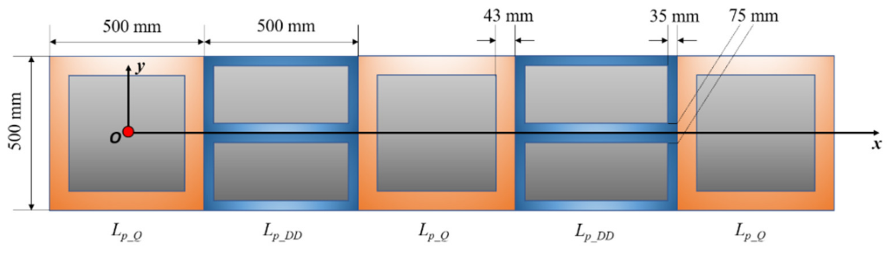
The detailed size of the transmitter array is demonstrated in
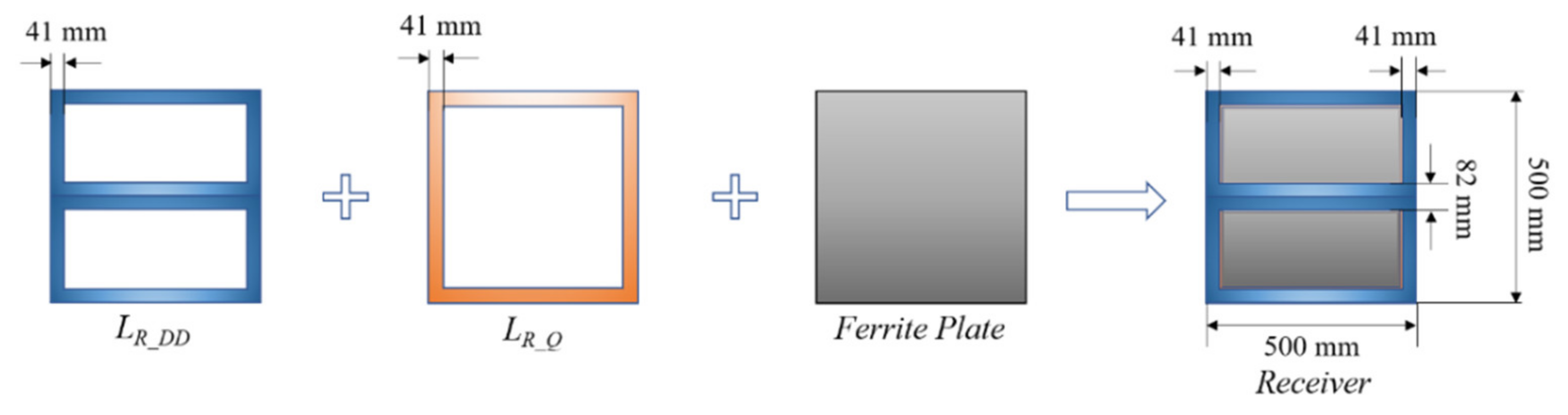
Figure 3. Because of the test size limitation, only five transmitters and one receiver are considered in this work. The receiver coil is designed with the same size as the transmitting coil, as illustrated in
Figure 4. Both transmitters and the receiver consist of LITZ-wire coils and ferrite plates. Furthermore, ferrite plates are the same size as the coil pads to improve the magnetic field and reduce flux leakage. Each ferrite core thickness is 10 mm, and the raw material is PC40 from TDK [
19]. In terms of manufacturing the inductors and the magnetic coupler, this work adopts the 1000-strand LITZ-wire with a 6.5 mm wire diameter. The advantage of multi-stranded LITZ-wire is its ability to reduce losses from the skin effect and proximity effect [
16].
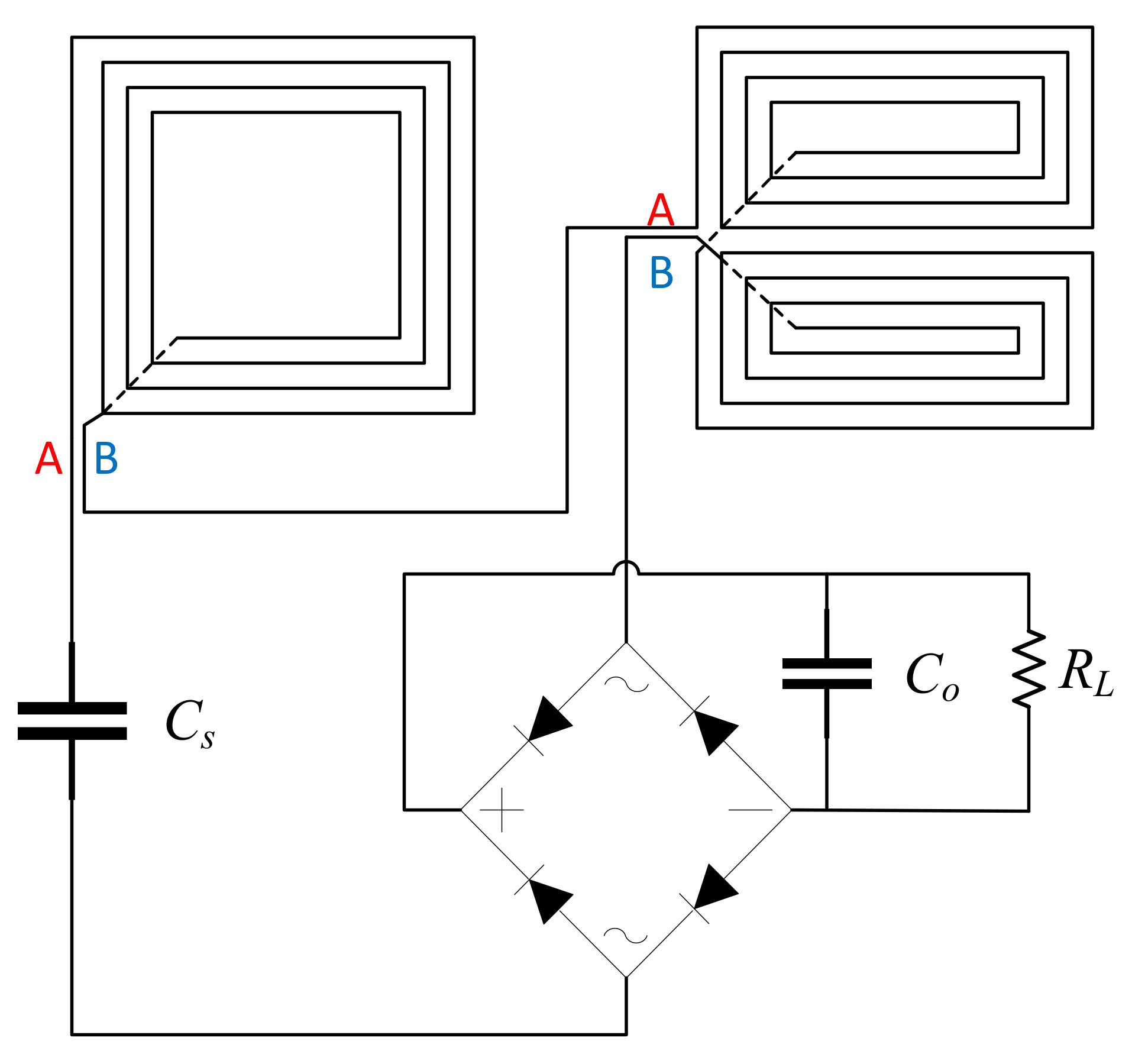
Even though the magnetic coupler shape has been presented in [
15], the coil connection method still needs clarifying because it plays an essential role in stabilizing mutual inductance. Specifically, there are two terminals, i.e., A and B, for each coil, as illustrated in
Figure 5. The exact coil connection method from this work is demonstrated in
Table 1.
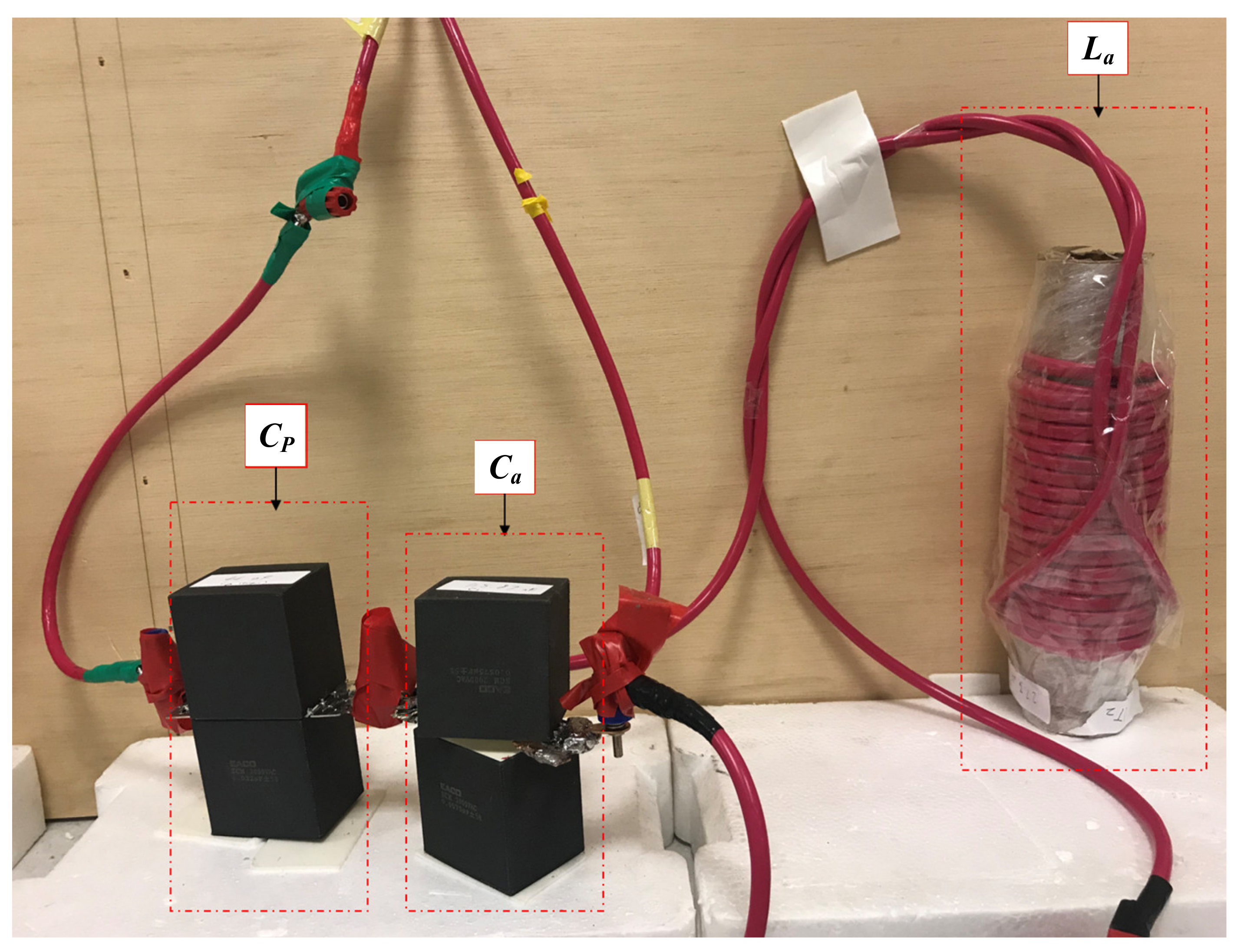
3. Circuit Analysis
As depicted in
Figure 6, the entire circuit system can be divided into two parts, i.e., the primary and secondary sides. The primary side consists of a high-power DC source, high-frequency inverters, and the
TX. The receiver part is composed of the
RX, a rectifier, and the load part. In this paper, five transmitters and one receiver are used for demonstration. Each transmitter coil works with the LCC unit that is made up of additional inductors
, additional capacitors
, and primary capacitors
. CV can be gained directly at the load side [
15]. The operating frequency is 85 kHz for industrial consideration, subject to SAE J2954 [
20]. The angular frequency should satisfy
In this paper, three inverters are used to power the transmitters. Due to the parallel connection, the phasor relationship of output voltage from the inverter can be expressed as [
21]
According to Kirchhoff’s current law (KCL), the current relationships can be gained as
Through manufacturing
delicately, the following equation can be revealed as
Similarly, it is easy to attain the relationships for the transmitting side by using Kirchhoff’s Law [
21]
Substituting Equations (2) and (4) into (5), the relationship can be rewritten as
which indicates that all the currents flowing through each transmitter coil
can be designed as the same value.
Furthermore,
Figure 7 depicts the equivalent circuit at the secondary side. The total induced voltage can be obtained as [
15]
where
is the total mutual inductance among segmented transmitters and the
.
is different according to different switching sequences, which highly depends on the number of energized coils. They can be expressed as
For stable switching operation, the average value of
should be equal to
with slight variation while
RX is moving.
is the total mutual inductance between
RX and all
TX coils, i.e.,
LP1 to
LP5. In
Figure 7,
because of the S-compensation network at the
RX side. Regarding the relationship between the input and output of the rectifier, it can be written as [
15]
Substituting Equations (6) and (7) into (9), the load-independent constant output voltage can be derived as
4. Switching Sequence
Only three transmitters need energizing in each segmented group. As illustrated in
Figure 8, the purple dotted line refers to the switching point line. In other words, the switching points include the −25 cm, 75 cm, and 175 cm points shown in
Figure 9. Due to the test size limitation, only the 75 cm switching point (
P2) is demonstrated in this work.
Silicon carbide MOSFET CCS050M12CM2 is adopted in the inverters, which ensures the high-power operation. The present design is to limit to one inverter to drive at most two transmitter coils in the experimental prototype to lower the current demand. The sequence of QDDQ is chosen as one segmented energizing group. The QDDQ refers to an energized group of three consecutive coils, i.e., a Q-shaped coil, a DD-shaped coil, and a Q-shaped coil again.
Furthermore, switching occurs when the right edge of the receiver directly faces the dotted line. In other words, switching happens where the receiver directly faces the Q coil transmitter. The periods of starting and ending are not considered in this article; the main concern is the period of stable operation.
Specifically, two-segmented energizing groups (e.g., G1 and G2) are built and demonstrated in this experimental test. G0 and other energized groups are neglected due to the size limitation of the test site. To be specific, G1 is conducted before P2. From P2 to P3, G2 is conducted, etc.
This article only considers the stable running period without the start and the end. The stable charging zone is from 0 cm to 162.5 cm, as illustrated in
Figure 9.
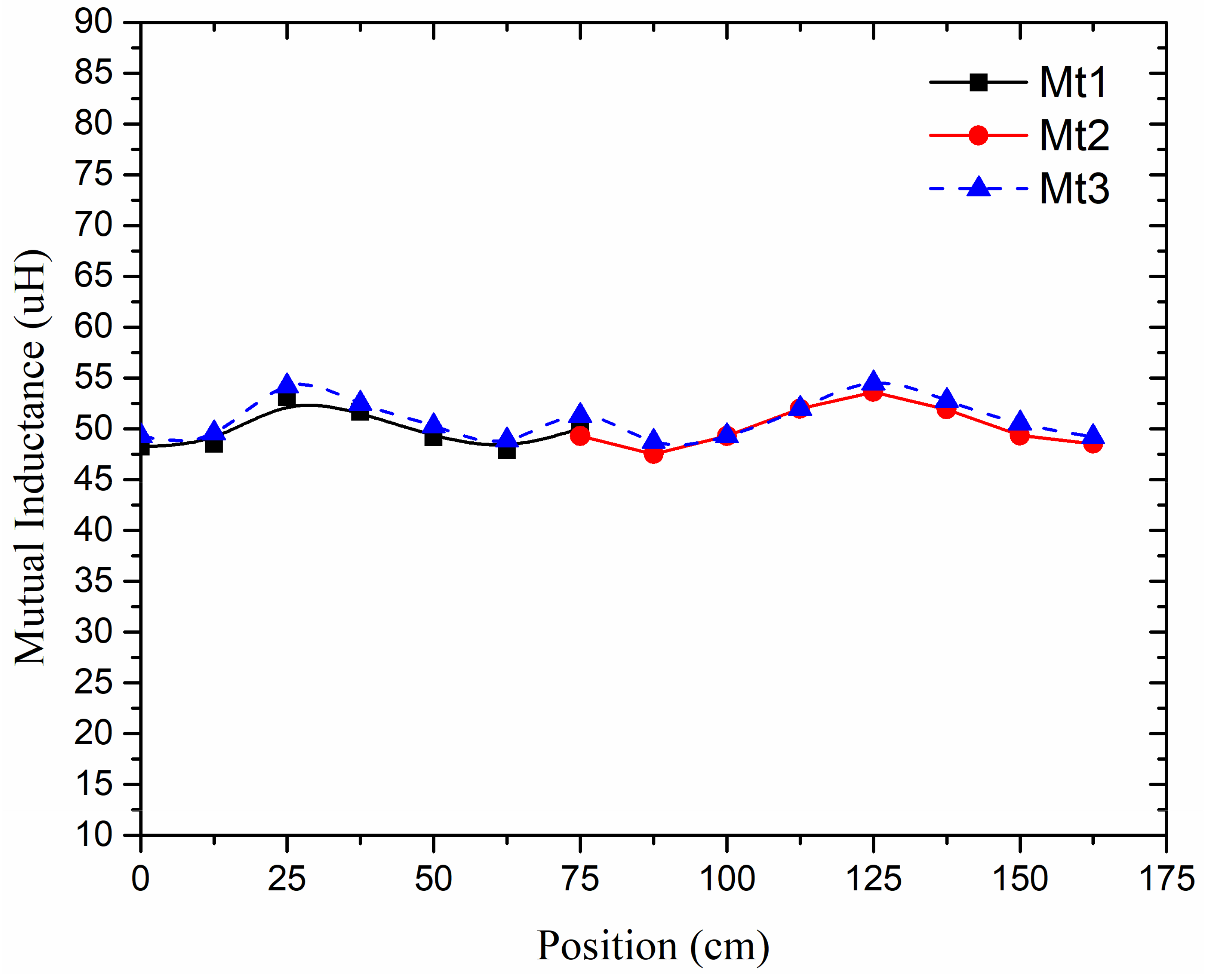
The mutual inductance between the
TX and
RX can be concluded in
Figure 10. Specifically,
is the total mutual inductance between the
RX and
G1 including
,
, and
.
is the total mutual inductance between the
RX and
G2 including
,
, and
. Finally,
is the total mutual inductance between
RX and all
TX coils from
to
.
This figure also illustrates that the magnetic coupling contribution from
and
is small during the
P2 to
P3 process. As demonstrated in
Figure 10, one QDDQ sequence after another can maintain the relatively stable mutual inductance, i.e.,
and
. Hence, the three-consecutive-coil group QDDQ can be selected as one segmented energizing group.
The measured value of total mutual inductance is changed from 47.5 µH to 53.6 µH. The minimum value occurs at 87.5 cm, whereas the peak value occurs at the 125 cm position. The average value of the total mutual inductance is approximately 50 µH.
After QDDQ, there is no need to energize DDQDD, i.e., a DD-shaped coil, a Q-shaped coil, and a DD-shaped coil. Firstly, the mutual inductance is already stable using the proposed sequence. Additionally, only one switch operation is required when using one QDDQ after another QDDQ. If using QDDQ, DDQDD, and then QDDQ again, three switching operations will be required for the same distance in this experimental prototype.
5. Experimental Verification
As illustrated in
Figure 11, a laboratory prototype of the proposed segmented DWPT system is built. This prototype consists of five transmitters and one receiver. The moving speed is assumed to be slow enough so that its effect on the segmented switch can be neglected [
15]. One DC power supply is adopted to power these three parallel inverters. Through the well-designed LCC units shown in
Figure 12, the load-independent CV can be achieved at the load side [
14,
15].
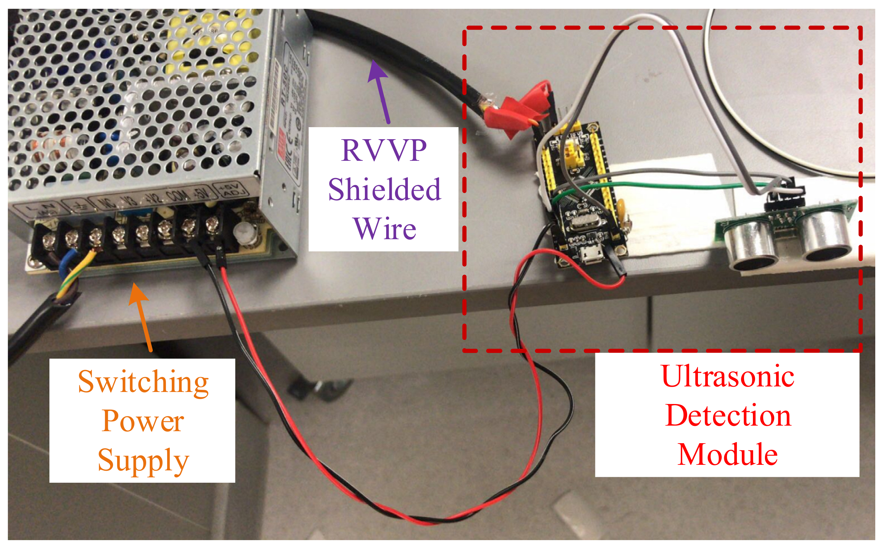
Segmented wireless charging can be achieved according to the positions of the receiver. The ultrasonic module HY-SRF05 can realize position detection with an RVVP shielded wire, as shown in
Figure 13, which ensures that the signal data cannot be interfered by the high-frequency magnetic field. The detailed parameters of the entire experimental prototype are listed in
Table 2.
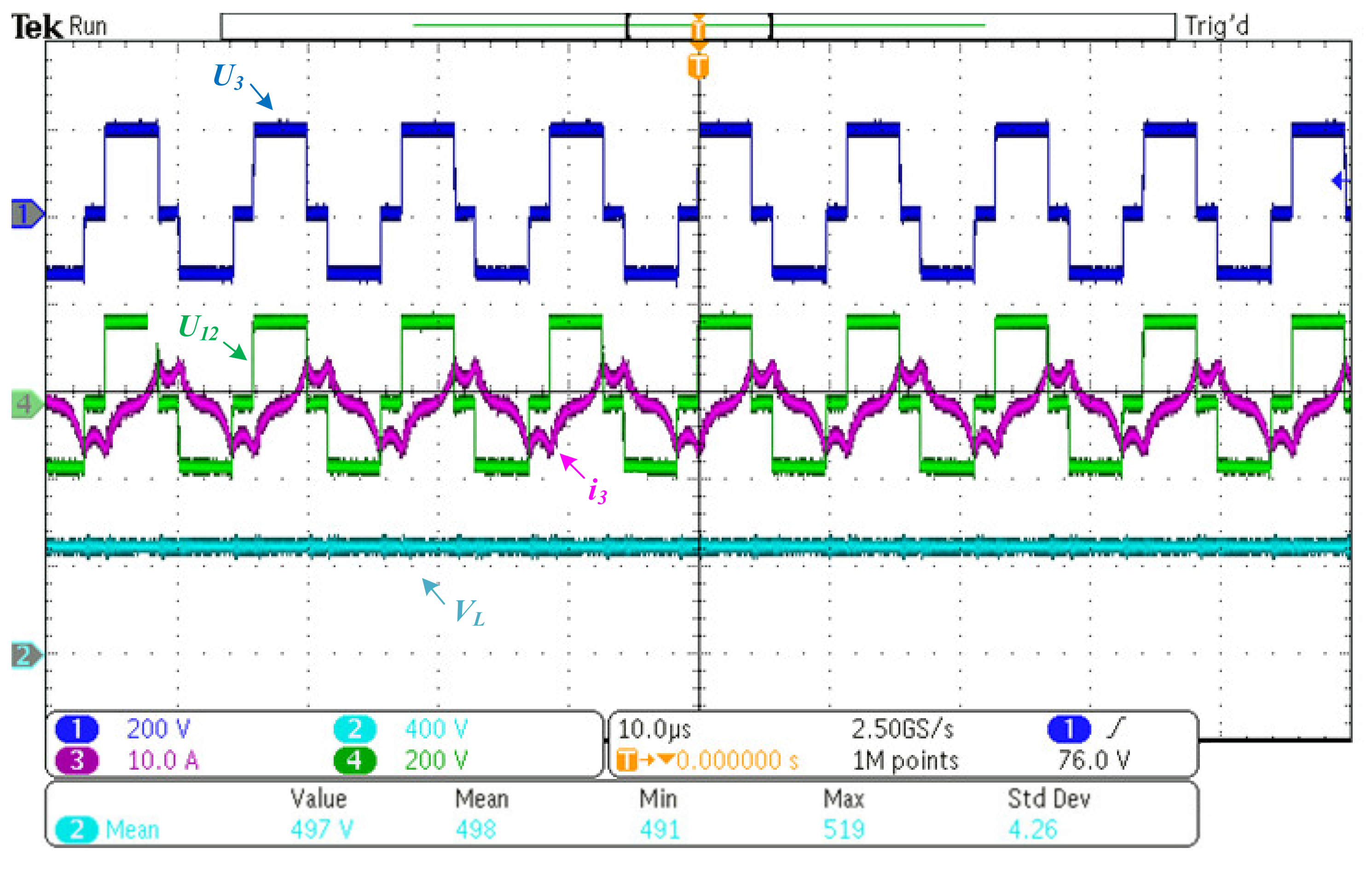
As illustrated in
Figure 14, the constant voltage can be maintained around 500 V through the whole operation period with slight variation.
Figure 15 and
Figure 16 describe the key waveforms before and after the switching point, respectively. Before the switching point,
is turned on, whereas
is turned off. After the switching point,
is switched on, whereas
is turned off.
is constantly turned on during the whole period because both
G1 and
G2 need
in this experimental validation.
The current distortion can be seen in
Figure 15 and
Figure 16, a problem that will be addressed in future work. The possible cause may be the slight change in resonant state caused by the secondary side while in motion.
Overall, load-independent 500 V output voltage is achieved with oscillation ripples under 25 V (5% of the nominal voltage).
6. Efficiency and Power Analysis
It is necessary to investigate the performances with different load values for practical use. In this article, the efficiency is the overall dc-dc power transfer efficiency defined as
where
Pin is the input power and
Pout is the output power. In this article, the input power can be directly gained from the DC power supply EA-PSI 9500-30. The output power can be calculated as
where load
RL is changed from 100 Ω to 200 Ω. The load voltage
VL is kept at 500 V. The 2.5 kW maximum output power occurs at the 100 Ω load condition. The output voltage can be directly measured by oscilloscope Tektronix MDO3024. Therefore, the measured values of overall dc-dc efficiency and the output power at different loads are shown in
Figure 17.
7. Benchmarking
Table 3 demonstrates the benchmarking among several segmented DWPT research projects and the findings described in this paper. Compared with [
8,
14,
15,
22], the proposed DWPT system achieves a high-power level, i.e., 2500 W, with refined energized transmitters.
8. Conclusions
Overall, this paper presents a high-power and high-voltage segmented DWPT. The maximum output power and voltage can achieve 2.5 kW and 500 V, respectively. This integrated and improved design offers a stable operation with refined transmitter coils. The well-designed magnetic coupler ensures safe operation for high-power applications. Parallel inverters are adopted to enhance the power level and reduce the voltage or current stress on semiconductor devices.
Furthermore, the QDDQ switching sequence is proposed. The connection method is clarified for Q-shaped coils and DD coils. Three transmitters, QDDQ, are energized in each group, which can ensure a stable operation. The proposed switching sequence also establishes a balance between the number of energized transmitters and the output voltage variation reduction.
A laboratory test using 85 kHz operation frequency was conducted. The experimental results show that the output voltage of the proposed DWPT is stable and constant while in motion. The dc-dc efficiency can reach approximately 85% from 100 Ω to 200 Ω loads. Future work will focus on resolving current distortion, improving the lateral misalignment tolerance, and achieving a zero-phase angle for the whole system.


