1. Introduction
The European project “Shift2rail” [
1] is investigating the advantages of the SiC wide bandgap devices in railway applications. The potential benefits of using SiC MOSFETs in future converters are explored, but also the mandatory impacts on the 3D layout design. With the high speed commutation of these new switches, there is a strong need of properly designing a geometrical arrangement of the various parts of a converter, in order to prevent all consequences of the stray elements originated from the cabling. Voltage overshoots, ringing, and power drive interactions are major concerns of power electronics designers in the “wide bandgap era” [
2,
3,
4].
Among the issues arising from high switching speed in high current applications, the current division among paralleled power modules is a key topic, which has to be addressed carefully to avoid any derating of the devices [
5].
Several parameters may generate a bad current division among power modules [
6]:
difference between device’s parameters due to industrial processes or different operating temperatures,
the power layout which provides various current paths among the paralleled devices and therefore different loop inductances, leading to a different current commutation speed (dI/dt),
the gate circuit layout, including the common emitter and the mutual coupling between gate and power circuits: both effects modify the gate-to-emitter voltage, and consequently the dI/dt.
All these phenomena have been investigated for many years for Si IGBTs, and more recently for SiC MOSFETs. The impact of power layout dissymmetry has been reported in [
7,
8,
9,
10]. It was shown that an electrical symmetry (i.e., equivalent loop inductance seen from each devices) can be obtained even with non-symmetrical geometries, taking into account the effect of mutual inductances. However, this necessitates many degrees of freedom for the 3D placement of the power modules, which are not always available in a railway inverter. Indeed, compact solutions are requested, and the cold plate of the cooling system often imposes the modules arrangement.
Another very important origin of the bad dynamic current division is due to the gate driver. Many papers have addressed the issue of the common inductance between power and gate circuits on the emitter (or source) pin [
11,
12,
13,
14]. Of course, this phenomena has mainly been studied for the internal layout of the power module, and has more impact on the current division among the dies than the difference between several modules. However, these papers also described the impact of the mutual coupling between gate and power circuits, which is another origin of power-drive interaction. In other words, reducing the common emitter impedance is not sufficient to avoid the feedback effect from power to gate during transients, and the impact of the magnetic couplings has to be considered. This has been done in [
15], where a metric has been defined in order for all the dies inside the power module to be submitted to the same feedback voltage from the power circuit. Therefore, using mutual couplings, and despite different values of common emitter inductances, all gate to emitter voltages during transients were identical, leading to the same dI/dt. Defining a gate circuit layout according to this metric was obtained, using an optimization process, for a fixed power layout.
Nevertheless, in a general situation, the current imbalance among power devices during transients combines both effects of power layout and power-drive interaction. To elucidate these joint effects, it is necessary to add the device’s behavior. This was done in [
16] to account for electro-thermal effects, the device’s parameters being modified with temperature.
The present paper will propose a full investigation of the impact of all inductive stray effects generated by both power and gate layout. It will be shown that a dynamic current imbalance generated by the power layout can be compensated by properly designing a gate circuit layout. The electrical equations developed in this paper are more or less similar to the recent work reported in [
17] and will be used in an optimization process to obtain an improved current division, despite the current imbalance caused by the power layout.
The approach to get the circuit equations must start with a clear link between the 3D geometry and the electrical representation. Partial Element Equivalent Circuit (PEEC) [
18] is today the classical modeling approach to reach this goal. It allows for the representation of any conductor with a partial inductance, and for mutual couplings with the rest of the circuit. However, if the transfer from a simple interconnection linking two points to its electrical model is straightforward, multiple port connections, as busbars, must be clarified. This paper will present a generic electrical representation for this kind of multiport conductors, which is implemented in many PEEC software but not reported in the literature so far.
To support the proposed method, a 1700 V 1200 A railway inverter,
ONIX 671, will be used as an example. Even if this inverter is not based on SiC devices, it exhibits some current imbalance, whose origin will be investigated thanks to simulation (
Section 2). In
Section 3, the generic circuit model derived from the 3D layout will be presented. Equations got from the model will be used to obtain a cabling rule to guarantee balanced currents during transients, despite a non-symmetric power layout. This cabling rule will be the objective function of the optimization process carried out in
Section 4.
2. Inverter Description
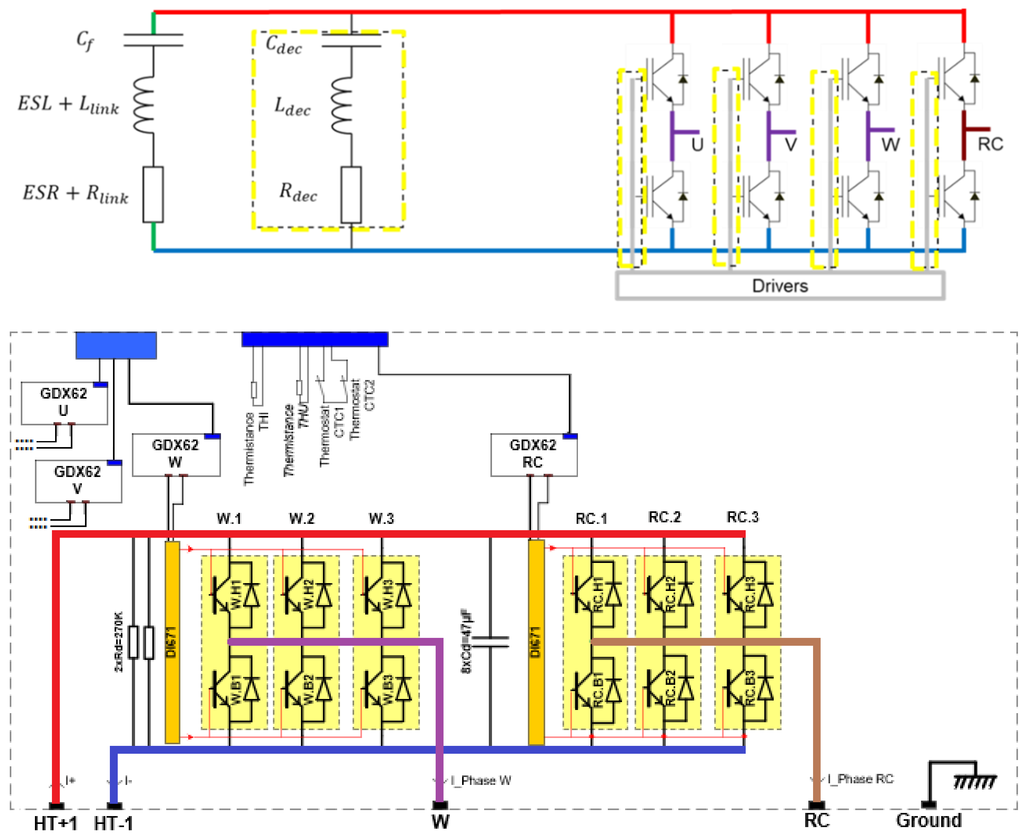
The 1700 V 1200 A studied inverter is a 3 phases + 1 brake chopper topology. The electrical representation of the inverter is given in
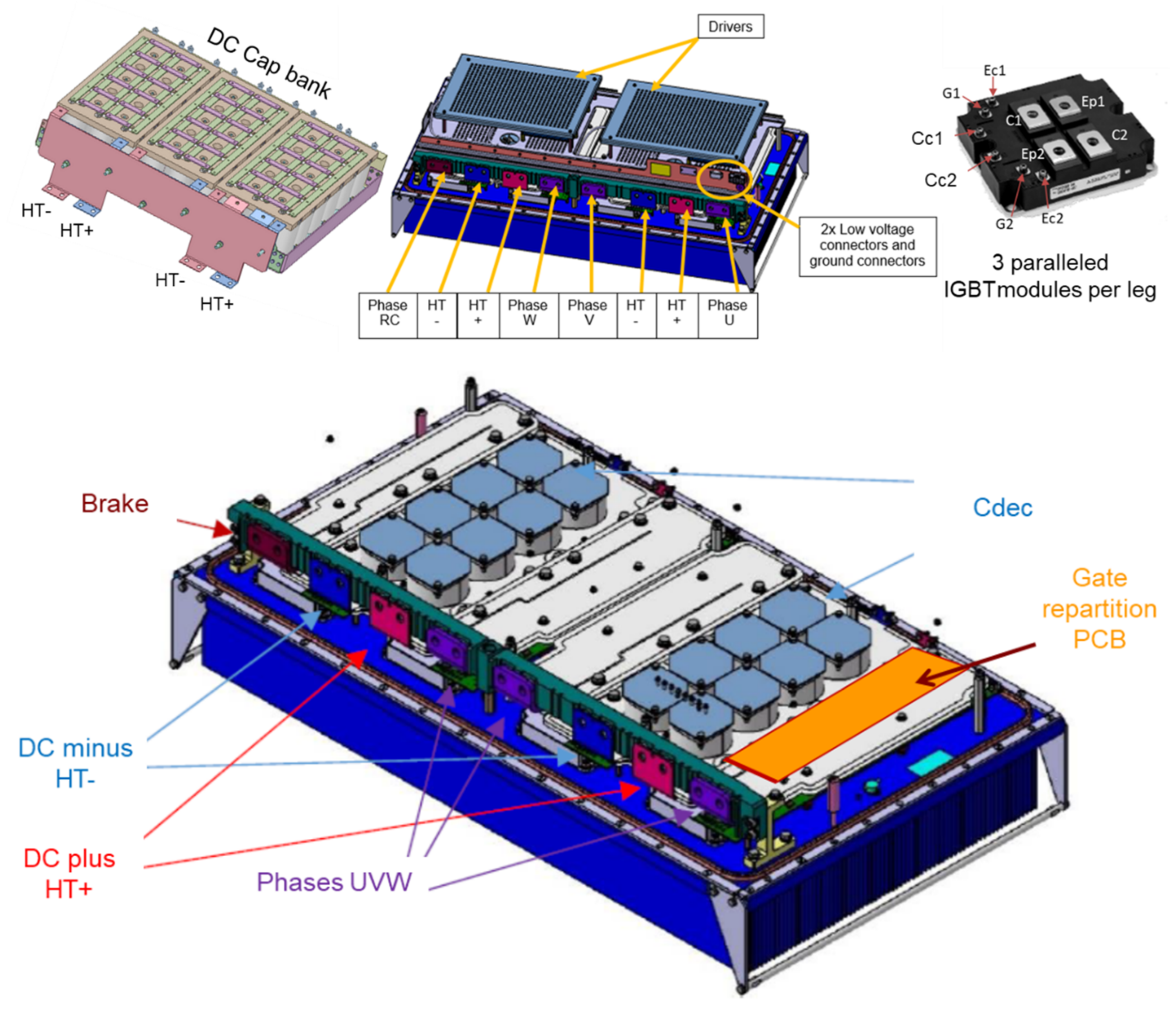
Figure 1, and the 3D layout in
Figure 2. Several parts can be identified:
An Electrolytic Capacitor Bank made of 54 devices (18 groups of three series capacitors), connected to the two HT+ and the two HT− terminals (DC bus);
two identical subparts, each of them realizing two legs. One sub part is composed of six power modules (three paralleled devices for top and bottom switches), eight decoupling capacitors, and three busbars for linking the aforementioned elements: one power busbar (DC bus) and two phase busbars for connection to the output phases.
Each subpart contains drivers for controlling the IGBTs. A specific Printed Cicuit Board (PCB) carries the driver signal to the three paralleled devices for the top and bottom switch of each phase. Two Gate Distribution PCBs are thus used for each subpart.
A cold plate is supporting all 12 power modules (dry natural cooling system).
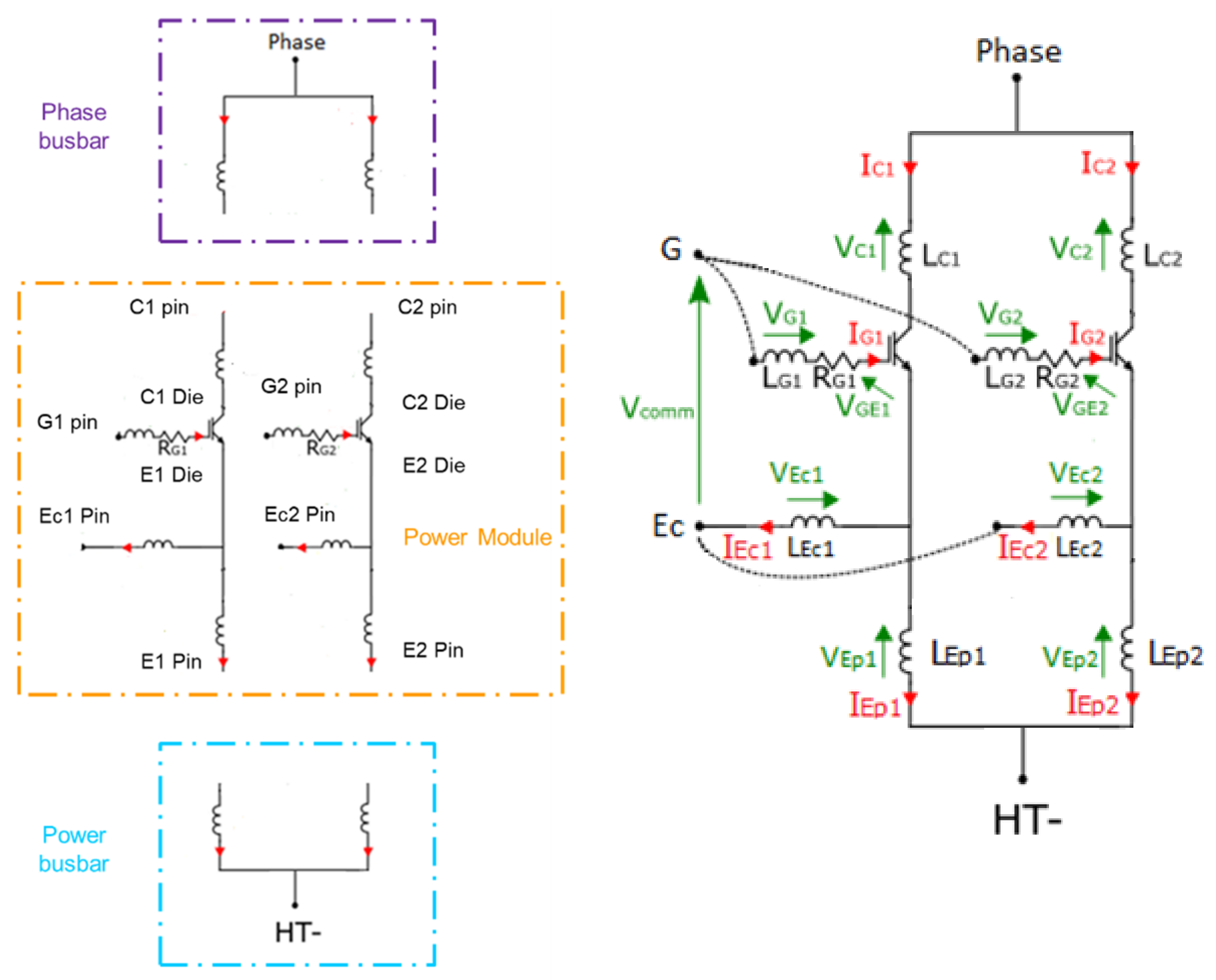
Figure 2 shows the 3D representation of the inverter. The Electrolytic Capacitor Bank associates three groups of capacitors realized with simple copper bars and is linked to the two inverter subparts through a dedicated busbar. The HT+ and HT− connections are therefore duplicated. The IGBT module is also displayed in
Figure 2. It offers separate Emitter and Collector pins for top and bottom switches (E1, C1 and E2, C2), the series connection being made by the phase busbar. A Kelvin connection is of course provided for each emitter of each IGBT (Ec1 and Ec2). Gate pins G1 and G2 as well as separate collectors Cc1 and Cc2 for control purposes are also indicated in the figure. On the bottom of
Figure 2, one can see the inverter power layout, which is split into two parts, each of them associating two inverter legs. For each subpart, six power modules are fixed on the cold plate and interconnected with a power busbar in the center and two phase busbars on both sides, which also provide the connection between all top emitters and bottom collectors of the three paralleled IGBTs. The power busbar associates the power module and eight decoupling capacitors, and provides links to the DC capacitor tank. The gate drivers are on the top, and a specific PCB is used for interfacing them with the three paralleled IGBTs. These four Gate Distribution PCBs are localized directly over the phase busbars.
The cold plate is not much larger than the 12 power modules. Therefore, there are almost no degrees of freedom for their geometrical implementation. The DC power busbar, linking the decoupling capacitors Cdec to the power modules, has to provide both small loop inductance and as much symmetry as possible for ensuring an equal current division between power modules. As mentioned before, the power modules are not providing the series association of the two IGBTs of the leg, and the electrical link between the Emitter of switch 1 and the Collector of switch 2 is performed through a part of the phase busbar. The switching cell is thus composed of Decoupling Capacitors, Power Busbar, and a part of the Phase Busbar.
It is worth noting that all phase busbars exhibit a slit, visible on
Figure 3. This one has been inserted for managing the static current division (DC resistance) between the three paralleled IGBTs. Indeed, the current path from the power modules to the phase output will have almost the same length, whereas without the slit the module close to the power connections would see a much shorter path than the most distant one.
In the experiment, the operations of this converter were not fully satisfying regarding the current division among the three paralleled modules. A huge experimental investigation was carried out to check if this current imbalance was due to the devices’ properties, but even when carefully sorting IGBTs with the same characteristics, the issue remained.
The 3D layout is thus at the origin of the bad current distribution among the three switches. Moving to SiC MOSFET with this kind of layout is not possible because the influence of the cabling will be much more important with a higher commutation speed. Understanding the root cause of the issue is therefore mandatory. For this purpose, an investigation using a simulation has been carried out, using Ansoft Q3D [
19] and the associated time domain simulator Simplorer.
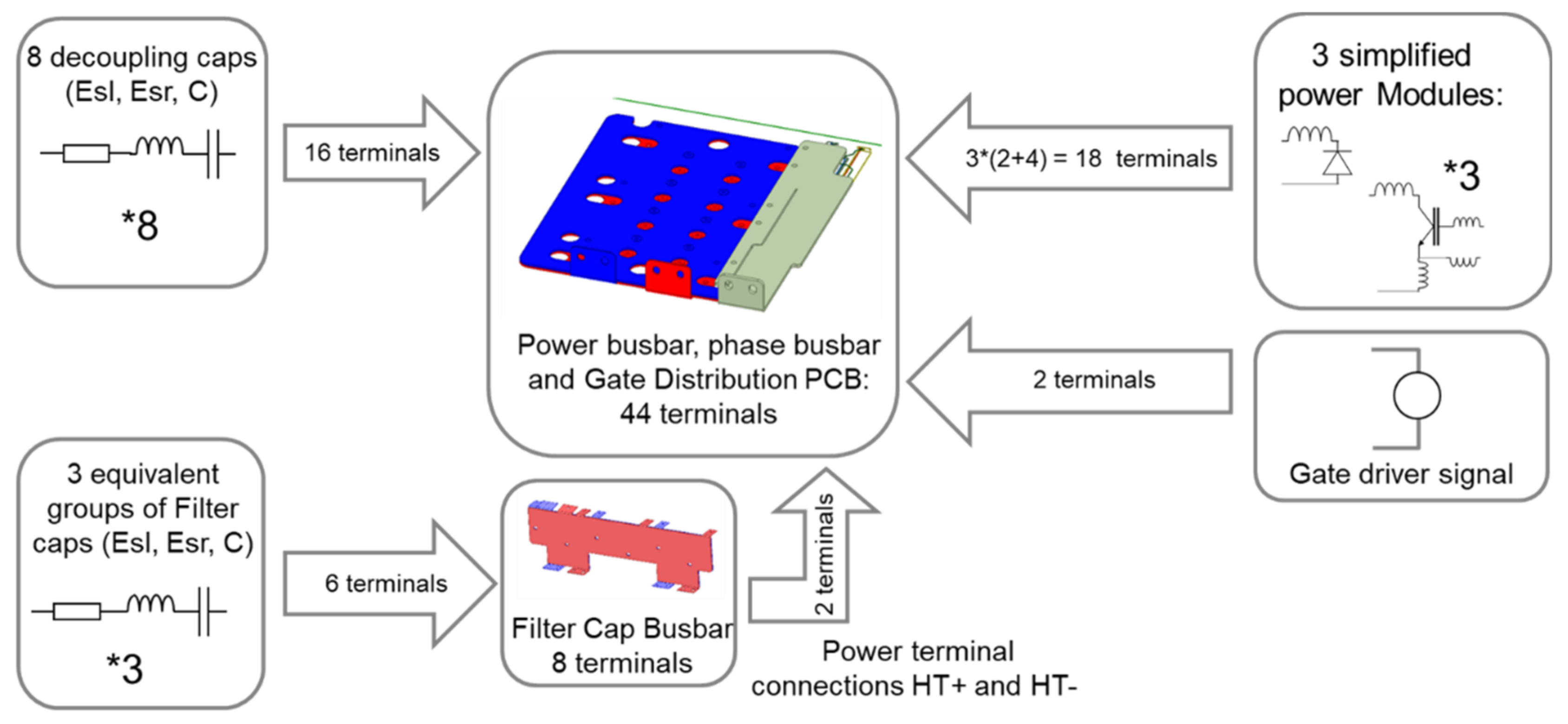
For this purpose, it was decided to focus on the bottom switch of phase W, composed of 3 paralleled IGBTs. The power layout is composed of the DC busbars and the phase W busbar. IGBT power modules have been simplified and represented by simple lumped inductances, to avoid overloading the 3D simulation model. This simplification is not a real issue, since all modules are identical: this is not the origin of the current dissymmetry. The eight decoupling capacitors have been identified through impedance measurement (simple esl–esr model [
20]) and their equivalent circuit is connected to the appropriate ports of the 3D PEEC model. The DC capacitor bank has also be simplified: from
Figure 2, it can be seen that the parallel association of 18 groups of three series capacitors is realized with three blocks of 6 * 3 series components. An equivalent model of each block has been identified (again, equivalent series inductance and resistance), and only the DC capacitor busbar (
Figure 2) has been modeled in Ansoft Q3D. The power busbar and phase W busbar are also included in the 3D description. It is worth noting that to save memory space, the DC capacitor busbar has been modeled in a separate file, since its mutual coupling with the rest of the power structure is negligible.
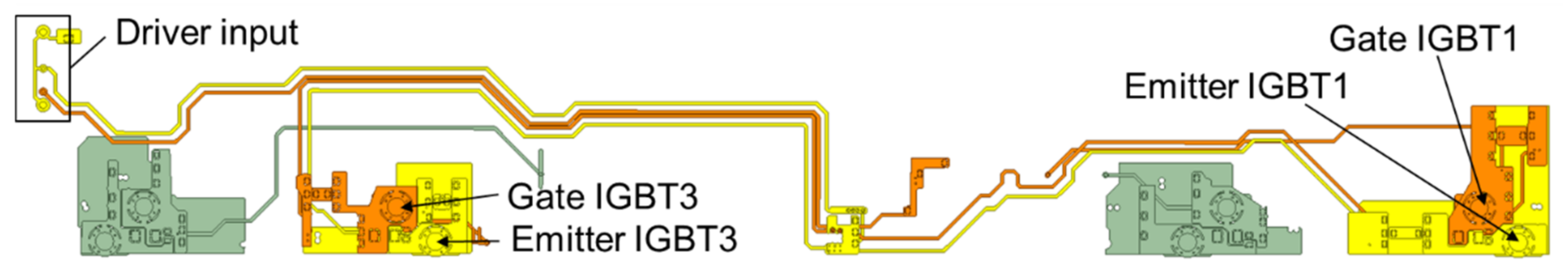
The gate driver is replaced by a perfect voltage source, common to each of the three paralleled IGBTs. The link between this voltage source and each of the three devices is made by the Gate Distribution PCB (
Figure 4 represents the part of this PCB corresponding to the bottom switches). It is a pure passive PCB, connecting the drive signal to each IGBT, and providing external gate resistances (some additional feedback and protection circuits are not studied here). It was included in the full 3D model, together with power and phase W busbars.
An illustration of the electrical simulation with all aforementioned blocks is provided in
Figure 5.
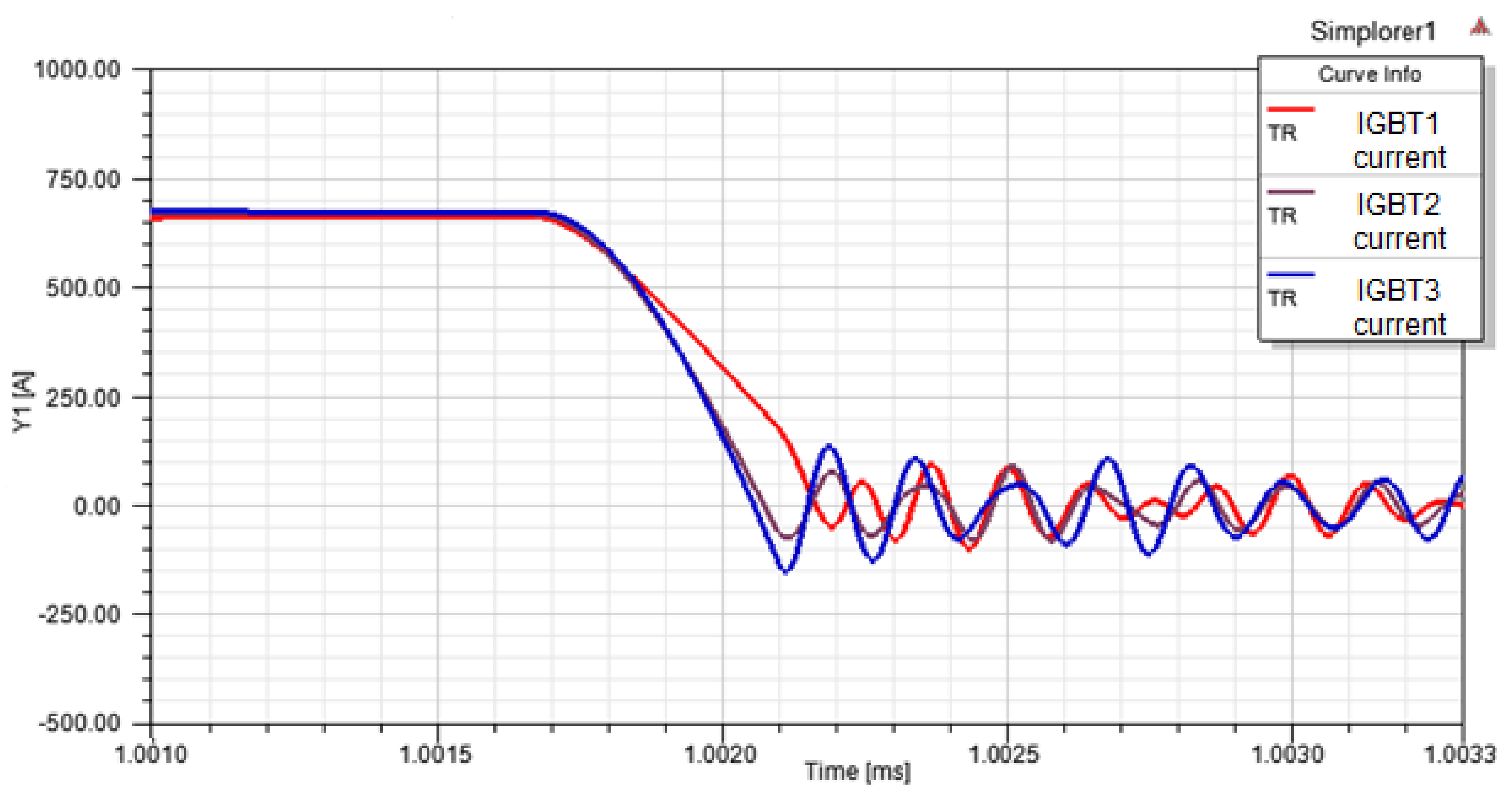
Figure 6 shows the simulation results for the three IGBTs. It is obvious in this figure that IGBT 3 (far from the phase output and close to the driver input) is slower than the two other ones, resulting in higher switching losses at turn off. IGBT 2 (in the middle) is the quickest one, and consequently takes the major part of the diode recovery current.
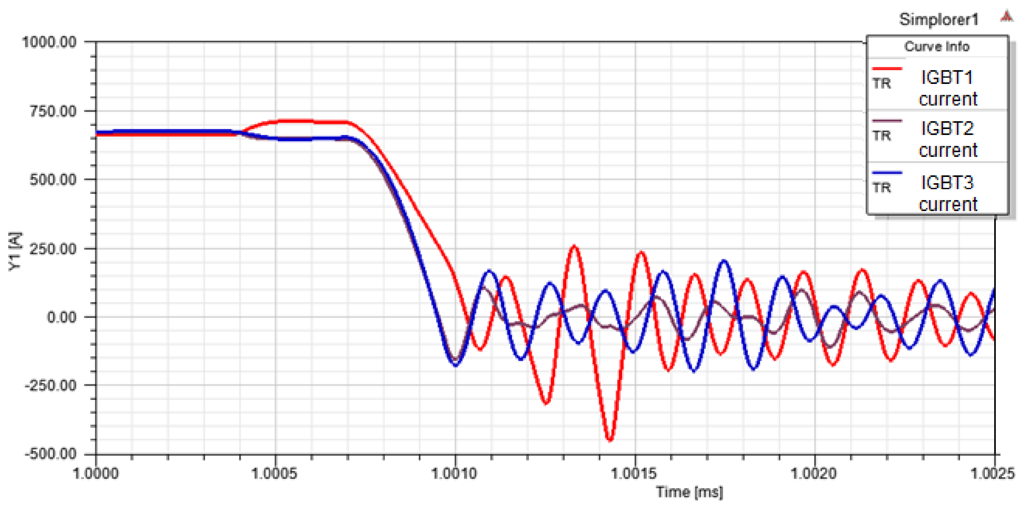
To understand the root cause of the imbalance and determine if was due to the power layout or to the power-drive interaction, a second simulation was done, removing the Gate Distribution PCB from the 3D representation and directly controlling the IGBTs by the ideal driver voltage source. Therefore, only the power layout was impacting the current division. Simulation results are given in
Figure 7. Again, current division is not perfect, but this time the slowest device is not IGBT3, as in
Figure 6, but IGBT 1. Therefore, the current imbalance is necessarily affected by both effects, power and gate circuits.
A last simulation was also carried out to confirm the impact of mutual couplings in the power-drive interaction. The Gate Distribution PCB was described in a separate file in Q3D, therefore keeping the effects of its impedance, but not considering the mutual couplings with the power layout. The results of
Figure 8 show that IGBT1 is still the slowest, as with the perfect gate circuit, which clearly shows that the most impacting effect is due to this coupling between Power and Gate Distribution PCB. This is not surprising considering the position of this PCB, directly on the top of the phase busbar, which is part of the switching cell, so carrying high dI/dt.
From these simulations, it can be concluded that:
the power layout generates a current imbalance, IGBT 3 being slower than the two others
the couplings between this PCB and the power part actually modify the current division, since taking them into account leads to a real change in the slowest device (IGBT 1 instead of IGBT 3). They must therefore be considered.
The power layout is hard to modify, due to a lack of space and the mandatory position of the power modules on the cold plate. It has been shown that it is generating a current imbalance, but that this one is reversed when considering the Gate Driver PCB. Therefore, there is a possibility to compensate the imbalance caused by the power layout, using the coupling with the gate circuit. However, to guarantee this compensation, it is first necessary to consider both effects in a circuit model, combining an electrical representation of the power layout, the gate layout, their couplings, and the IGBT model. This is the aim of the following section.
3. Electrical Model of Paralleled IGBTs
Obtaining the circuit model from a 3D layout is quite straightforward using the PEEC approach for a simple conductor linking two points: the conductor is replaced by a resistance, an inductance, and mutual coupling with the rest of the circuit. However, in the kind of 3D geometry used in
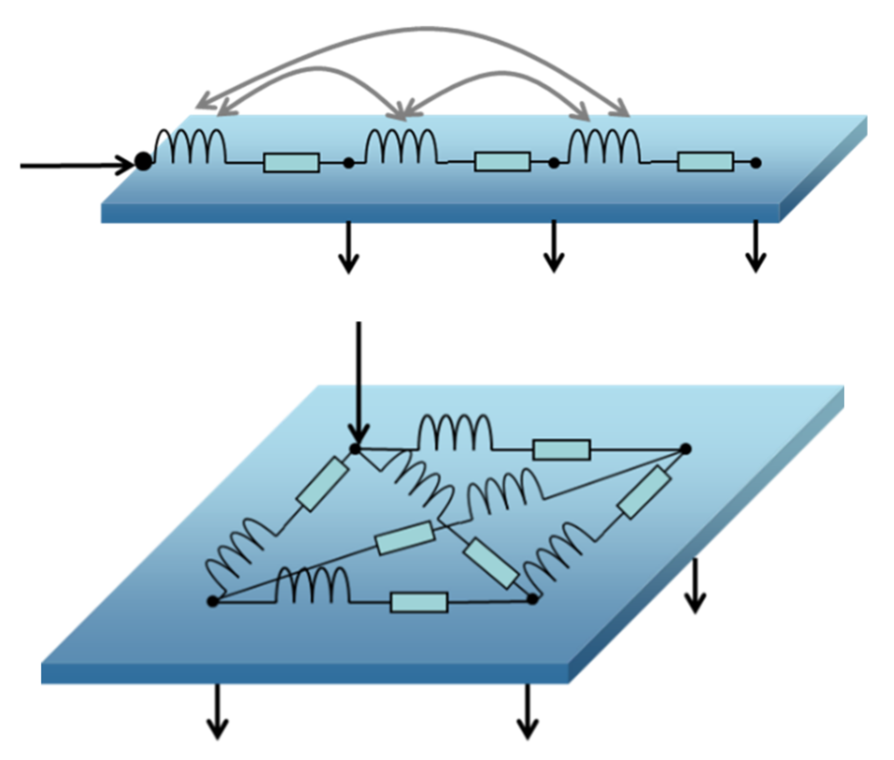
Figure 2, some conductors—as busbars, for instance—are not linking only two points but several points. Consequently, the electrical representation becomes tricky. In some cases, the geometrical layout is organized in such a way that the user can “guess” a circuit representation almost corresponding to the current path and the layout (
Figure 9 top). However, in the case of plates, for instance, the current path is unknown, and the equivalent circuit topology not straightforward. A possibility would be to connect all points with R-L coupled circuits, as in
Figure 9 bottom, but this is clearly not the representation using the minimal number of elements. The first subsection will propose a generic approach to get an electrical circuit from the 3D layout, based on a “terminal behavior” vision. This generic representation is used in several existing PEEC softwares, as Ansoft Q3D [
19] or Altair Flux-PEEC [
21], but has not been explained in such detail so far.
This circuit representation of both power and gate circuits will be combined with an IGBT conventional model in order to investigate the current division in the simplified case of two paralleled IGBTs. From this analysis, a rule on the impedance matrix will be derived to reach balanced currents in each IGBT.
3.1. Generic Circuit Representation
The results of the previous sections show the importance of considering all stray inductive elements involved in the dynamic behavior of the switching, including power, layout, and mutual couplings with the gate circuits. It is thus mandatory to take all of them into account. For simplification and illustration purposes, only two paralleled power modules will be considered in this section, even if, obviously, the generalization to three and more is quite straightforward with the proposed equations and matrix writing. We will focus on the IGBT 1 and the IGBT 3 of the bottom switch of phase W to illustrate the geometry.
The chosen electrical circuit representation of a conductor linking N_port > 2 will be composed of N_port-1 inductors and resistors. One point among the I/O ports will be considered as a reference and linked with the others with R-L circuits (and couplings). The reference point can be chosen arbitrarily.
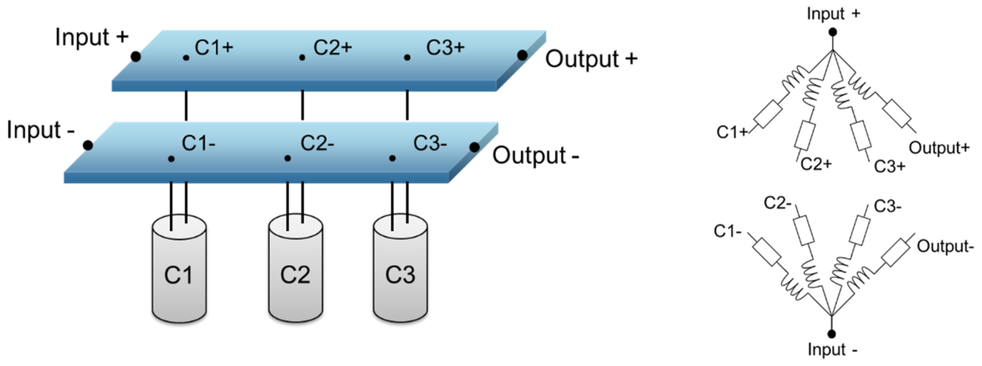
Figure 10 shows a simple illustration for the basic case of two plates associating three capacitors in parallel.
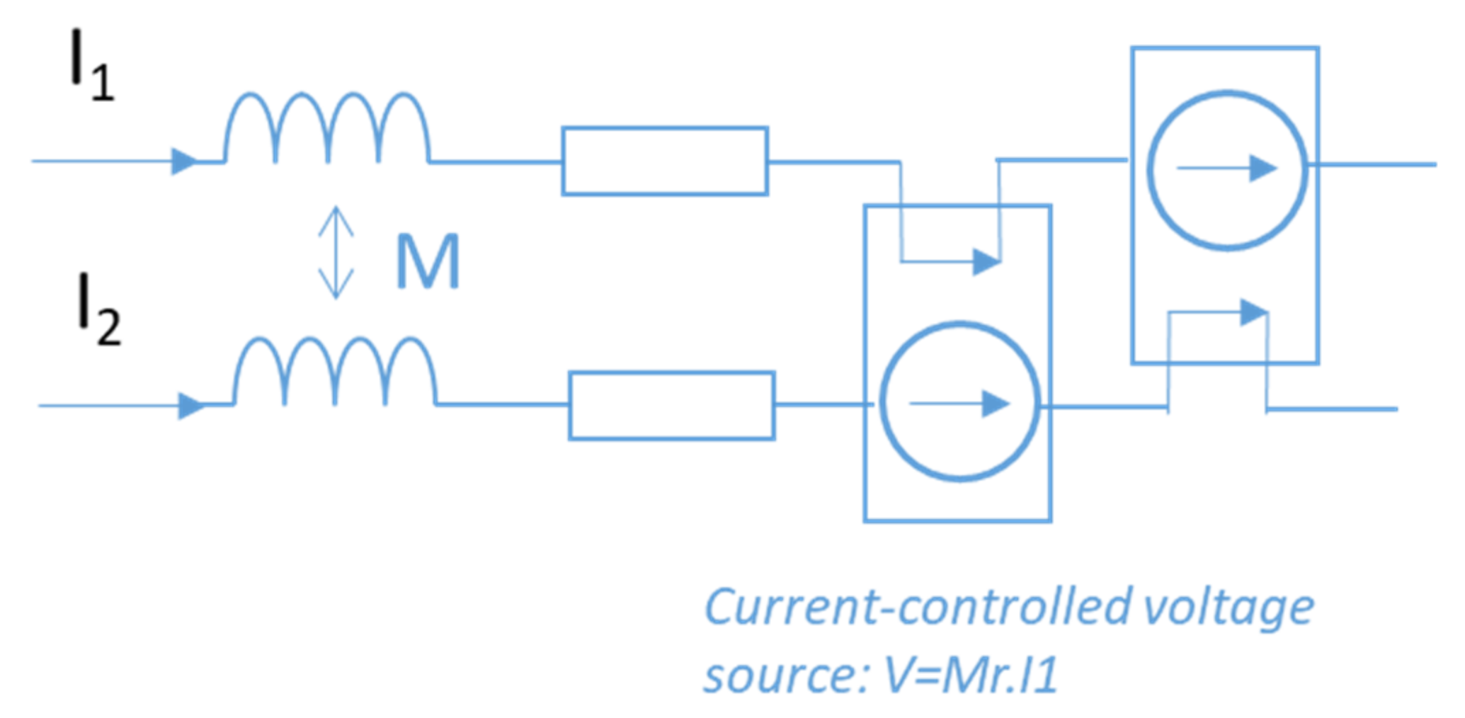
It is worth noting that this method is the one used in most PEEC-based softwares to generate Pspice-compatible netlists. One further remark is that in this representation, the full PEEC matrix exhibits both a real and an imaginary part. In other words, not only the inductors but also the resistors are coupled. Physically, this corresponds to a common resistive path within the same conductor and eddy currents induced in the rest of the geometry. These “resistive couplings” can be represented in circuit equations with current-controlled voltage sources (
Figure 11), or by writing differential equations in a programming language (VHDL AMS or MAST for Saber software).
3.2. Application to Two Paralleled IGBTs
Let’s consider two paralleled IGBTs connected between phase W and the HT− negative potential (IGBT 1 and IGBT 3 of the full geometry). The PEEC method was applied to model the power busbar as well as the phase busbar W. The power module was also described using a PEEC model.
For the power busbar, the phase W connecting terminal was chosen as reference point for linking it to both collectors C1 and C2, and the HT− potential for linking to both power emitters, E1 and E2. For the power module, collectors and gate pins are simple connections linking the die to the external pin. Only Emitters have to be linked to the Die, Control Emitter, and Power Emitter pins. In this case, the reference point was the emitter die. Therefore, the circuit of
Figure 12 left can be obtained, which can be reduced to the circuit of
Figure 12 right by associating all impedances in series.
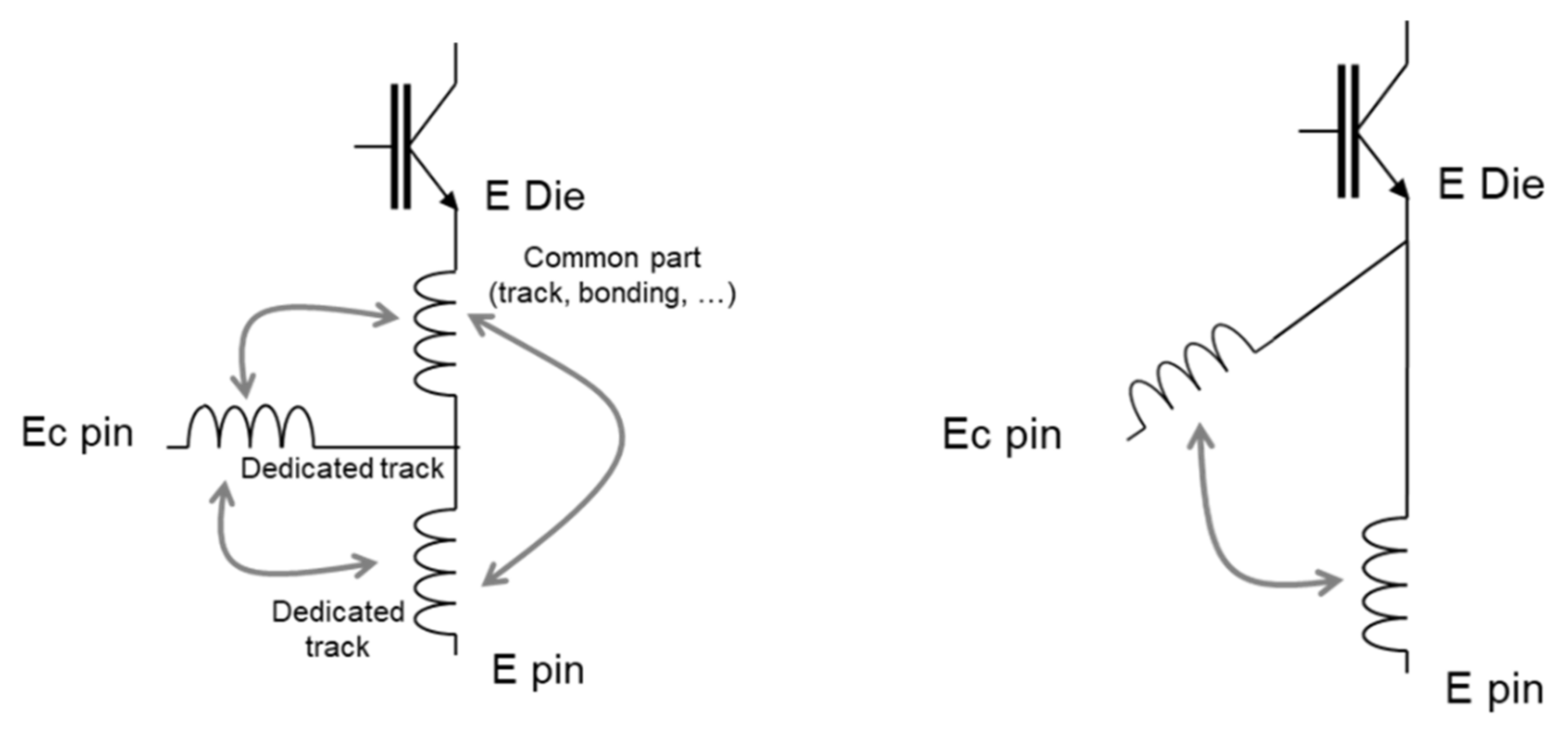
An important note is that this arbitrary circuit representation does not correspond to the geometrical layout: for instance, a part of the circuit can be common to the power and gate parts in the module (the contribution of a portion of DBC or bondings). This is not seen as a common inductance in the equivalent circuit of
Figure 12, but it is taken into account in the value of mutual impedance between stray elements. This is illustrated further in
Figure 13 for more clarity. In this figure, a part of the emitter path is common to the power and gate circuits. A geometrical representation would be as in
Figure 13 left, but the generic representation is always the same whatever the layout geometry.
3.3. Circuit Equations
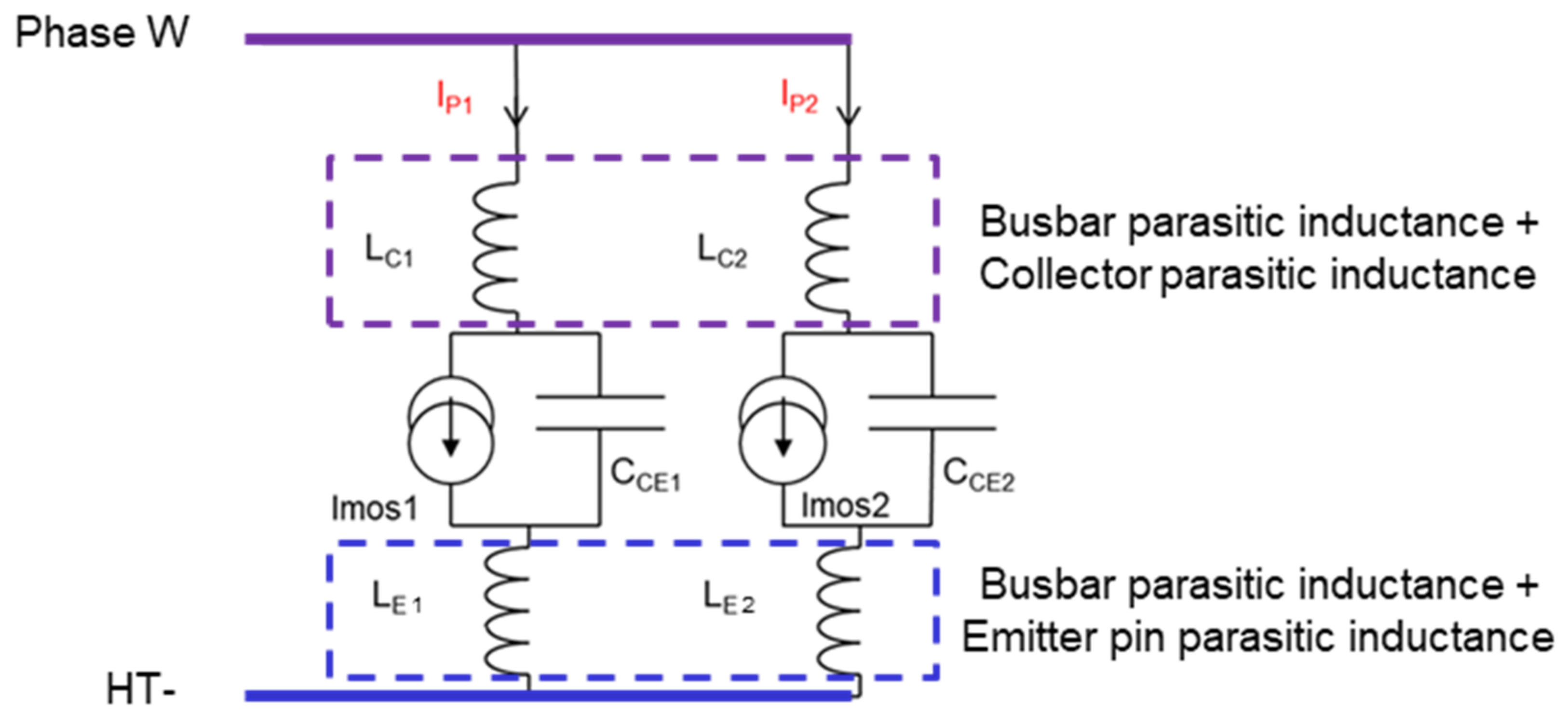
The method starts with considering the power circuit only, including a semiconductor model composed of a current source and the output capacitor, as illustrated in
Figure 14.
To simplify writing, only inductive elements are displayed and considered in the equations, but all resistive elements and resistive couplings could be easily taken into account.
The expressions of the two power currents,
IP1 and
IP2, can be written as follows.
with
according to the notations of
Figure 10 right, keeping the power elements only.
Considering identical devices,
CCE1 =
CCE2, gm
1 = gm
2, and
Vth1 =
Vth2. Furthermore, instead of solving the equation in the time domain, the frequency domain is preferred. Therefore, it leads to
Finally, combining (8) and (9), we obtain
Considering that the dynamic current share phenomena involves only high frequencies,
CDS.a.ω2 >> 1 and
CDS.d.ω2 >> 1. If we want to have
IP1 =
IP2, it leads to
This means that to obtain an equal dynamic share despite dissymmetric layouts, it is possible to act on the gate voltages in the following way:
with
It is worth noting that if the power layout is symmetrical, a = d and b = c; therefore, α = 1 and thus VGS1 = VGS2: it is not necessary to compensate the power currents from the gate side.
Once the power layout has been defined, the current dissymmetry is defined (i.e., a, b, c, d, and thus α), and it is possible to modify the gate circuit, in order to obtain different values of VGE1 and VGE2.
These gate voltages can be expressed as a function of gate and power currents and the various stray impedances of the circuit from
Figure 12 right:
ZG being the stray impedance matrix on the gate distribution PCB,
Vdriver being the driver output voltage (common for all devices), and
ZPG being the coupling matrix between gate distribution PCB and power circuit. This coupling matrix contains all mutual impedances the between power and the gate circuit, as already explained to introduce
Figure 12 right.
Neglecting gate currents in comparison with power currents leads to focus on
ZPG only. Therefore, the following expressions can be obtained for
VGE1 and
VGE2:
If we want to obtain
IP1 =
IP2, combining (11) and (12) with (9) leads to:
the summation term is just here to show that more than two paralleled devices can be considered.
Therefore, to reach equal currents, the
ZPG matrix has to be designed in such a way that (13) is fulfilled, in order to compensate the power dissymmetry, expressed by a non-unity value of α. In other words, all couplings between gate PCB and power layout should be designed in order to compensate the non-ideal behavior of the power part. This is a major improvement in comparison to previous works where only power dissymmetry [
7,
8,
9,
10] or power-drive interaction [
11,
12,
13,
14,
15] were considered, but not the possibility of compensating power dissymmetry through the gate circuit layout, using the device’s model, as in [
16,
17]. This target will be reached through optimization in the following section.
4. Optimization of the Gate Distribution PCB
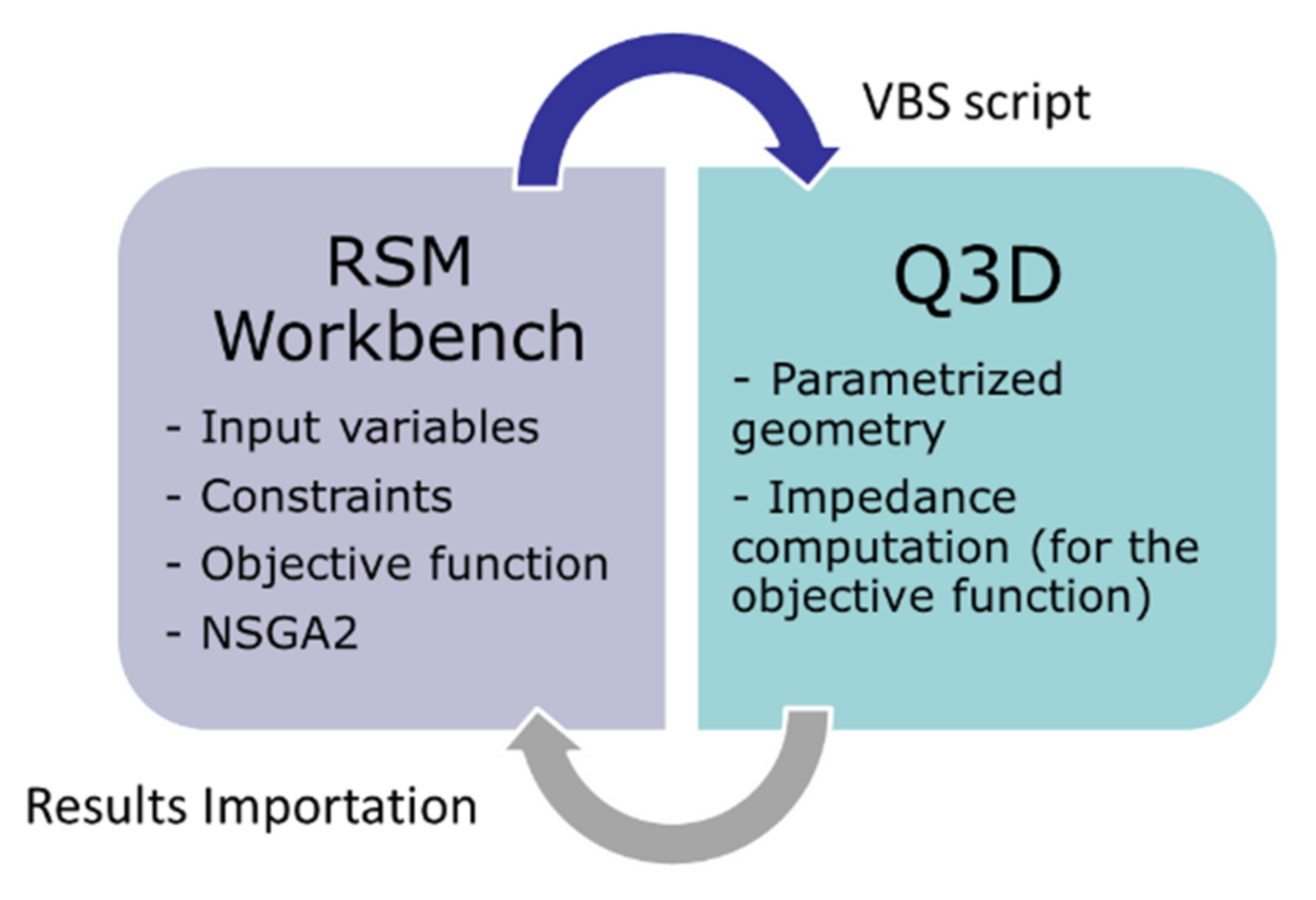
Finding the layout of the Gate Distribution PCB which, coupling with the power circuit, fits (13) is not possible with a human brain, even with years of trial-and-error work! Therefore, an optimization algorithm has been set up. The principle is illustrated in
Figure 15: a home-made optimization environment (RSM, developed by the Alstom group, Semeac France), controls the Ansoft Q3D PEEC software, in which a parametrized geometry of the Gate Distribution PCB and the power layout is described. By varying the geometrical parameters of the PCB, the objective function defined by (13) is minimized. The optimization used in the RSM environment is based on genetic algorithms NSGA2 [
22] and will not be described in this paper. The parametrized geometry of the Gate Distribution PCB is given in
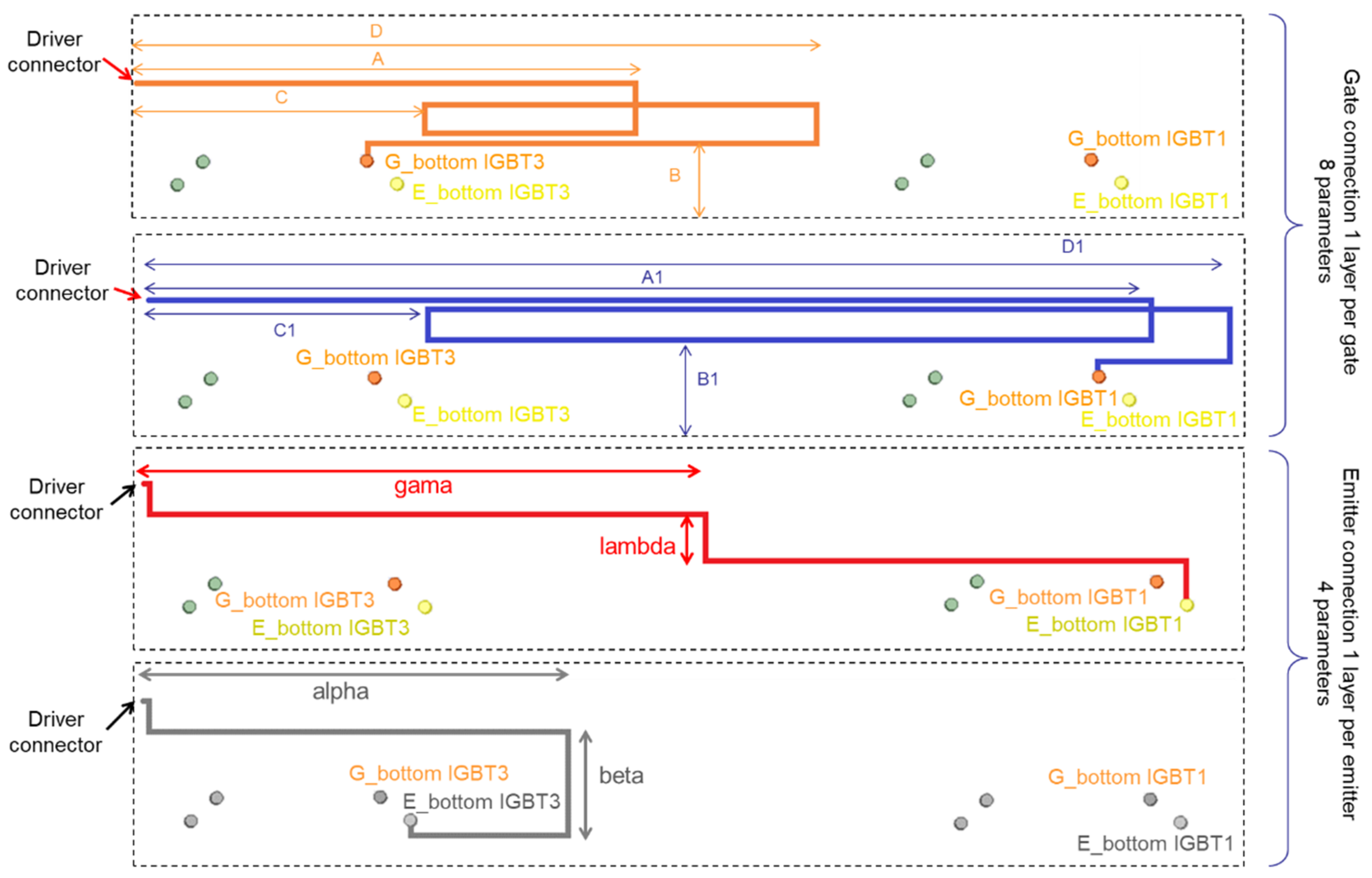
Figure 16. For simplicity, a multilayer description has been chosen, in order to draw the two gate tracks and the two emitter tracks independently. Track crossing in each layer is also allowed, to simplify the description. After optimization, the number of layers can be easily reduced, and track crossing can be avoided using vias. The geometrical description of the gate connections involves four parameters per gate, whereas the source connections are simpler and defined using two parameters per IGBT. Parameter description and an example of corresponding geometrical constraints are given in
Figure 16 and
Table 1, respectively. Choosing these 12 parameters allows the layout building some “loops”, which can provide positive or negative couplings with the power part, and thus allow sufficient degrees of freedom for the algorithm to reach the goal defined by the objective function. All connection points to the power modules are obviously fixed, since the power layout and the module location remain unchanged.
The optimization function is frequency-dependent: first of all, because equations were written in the frequency domain, and also because impedance evaluation in the PEEC software is carried out at a specific frequency. Since the goal is to balance currents during the switching phase, an equivalent frequency corresponding to the switching time, 0.35/t
switching, has been used [
23]. It has been evaluated to 50 MHz. The impact of this choice will be discussed later.
The main interest of the proposed method is that it does not imply any time simulation in the optimization loop, which is really time-consuming and often generates convergence issues: some configurations generated by the optimizer may indeed not be able to converge in the time domain, and the optimization process may thus fail.
After several hours of optimization, which is quite a reasonable amount of time, since the process is automatic, a result has been obtained. It is displayed in
Figure 17. The geometry displayed on the top of the figure is compatible with the imposed constraints (fixed connection points and maximum size of PCB).
On the bottom of
Figure 17, the evolution of the objective function is plotted as a function of the number of iterations of the algorithm. This representation helps in evaluating the convergence of the NSGA2 algorithm. It can be seen, for instance, that after iteration 400, the minimal value of the objective function has been reached and is not really modified between 400 and 1050, where it has been stopped. This minimal value converges up to 225,000, which is lower than the initial value, around 260,000. This objective function is the left part of (13). It has not reached zero due to all the constraints, but it has been reduced compared to the initial situation.
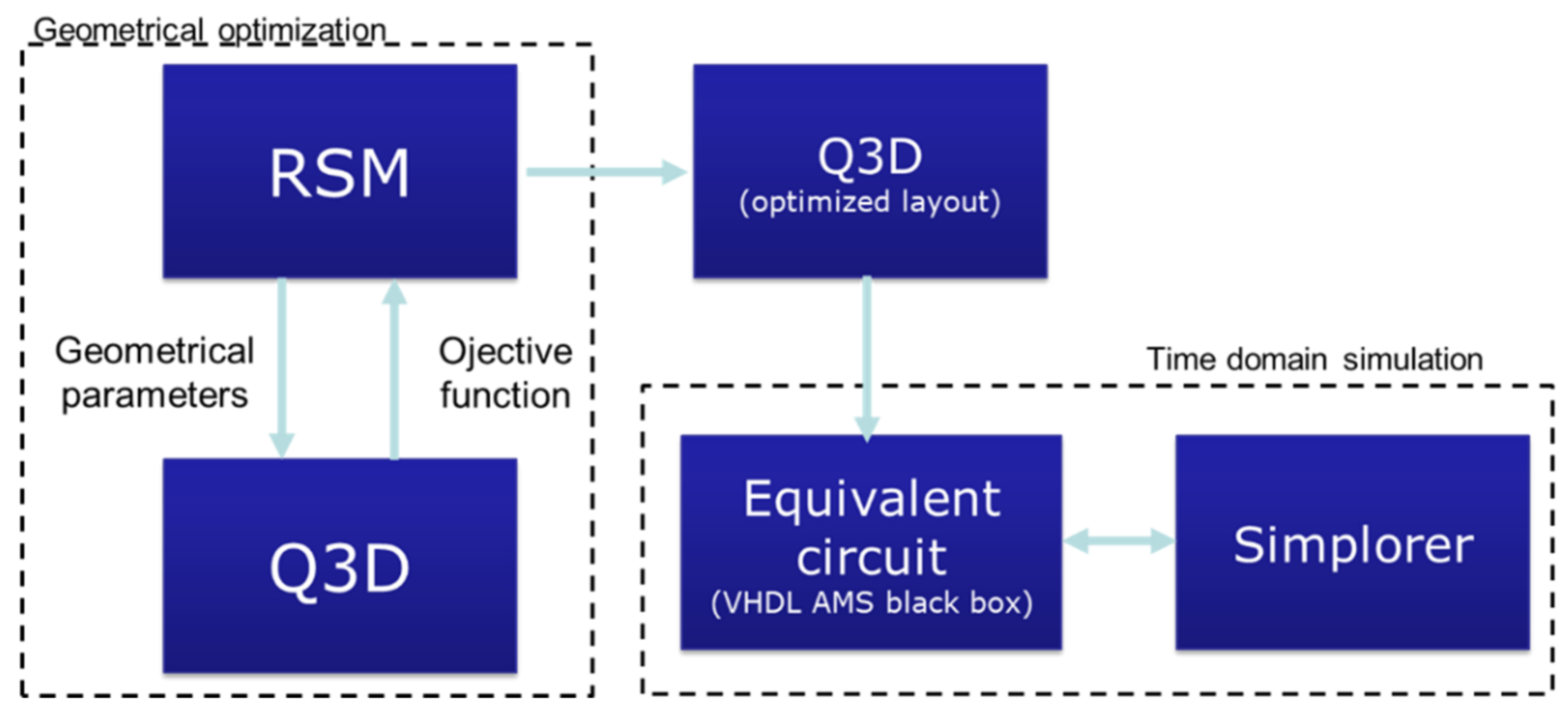
Since some assumptions have been made to build the objective function, and since it has been evaluated at a specific frequency (50 MHz), there is a strong need to validate the obtained result in the time domain. For this purpose, the PEEC model of the 3D layout (power and gate circuit in the same file for including couplings) has been combined with precise models of IGBTs in the Simplorer time domain simulator (
Figure 18).
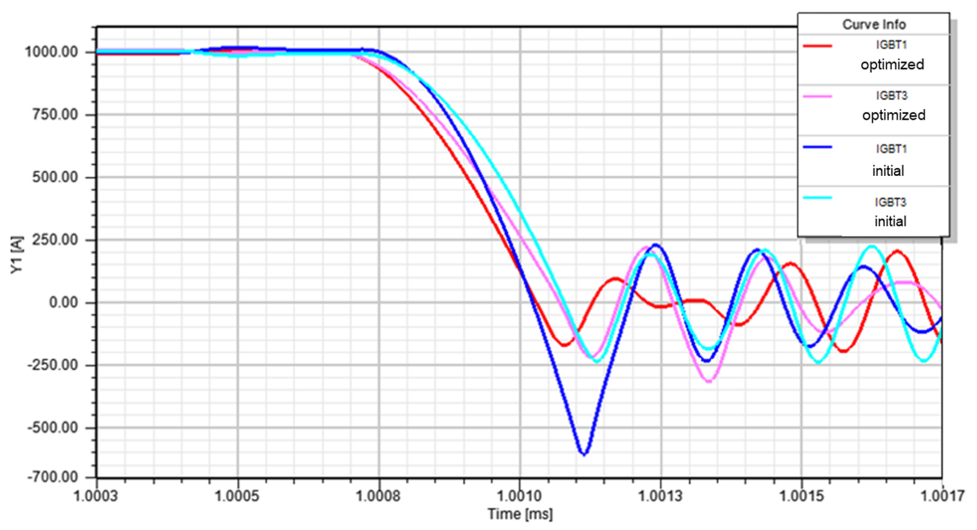
The initial geometry of the gate distribution PCB and the power layout has been simulated as well (light/dark blue curves in
Figure 19). Results are compared to the optimized gate distribution PCB (magenta/red in
Figure 19). The improvement is really obvious, which validates both the methodology and the optimized geometry.


 ,
, 


