1. Introduction
Semiconductors play an important role in solar cell technology, where the solar cell’s main parameter is high efficiency. The reported efficiency of the single-junction solar cells is low, and the multi-junction solar cells (SC) represent the most efficient approach to photovoltaic energy conversion, reporting an efficiency of around 40%. The multi-junction structure is designed based on the selective absorption of different significant parts of the solar spectrum. Different absorbers in cells improve the photogeneration and collection of minority carriers and reduce energy losses related to hot carriers’ thermalization [
1]. As the illuminated light enters the cell, the short and long wavelengths are absorbed in the top and bottom cells, respectively.
In a multi-junction solar cell, the cells are interrelated by the tunnel junctions to align the Fermi level. The tunnel junctions should have less electrical resistivity, a high optical transmission, and a high peak tunneling current density. Without the tunnel junction, the p-region of the top cell and n-side of the bottom cell directly connected, and the p-n junction in the opposite direction appears between cells. Therefore, the photo-voltage would be decreased. In theory, the generated electrons in the top cell and holes in the bottom cell will recombine in the tunnel junction, while the generated holes and electrons in the top and bottom cell will go through the load to form a complete current loop [
2,
3].
InGaP, which has a wide bandgap of about 1.9 eV and GaAs with 1.42 eV bandgap energy, are suitable for the top and bottom cells of highly capable multi-junction solar cells. The combination of the InGaP (top cell) and GaAs (bottom cell) has around 40% efficiency. The lattice parameters and photogeneration current of top and bottom cells can be coordinated when two cells consent together by the tunnel junction [
3]. However, the lattice and current mismatch are two critical factors that lower the conversion efficiency of multi-junction solar cells. In the InGaP/GaAs dual junction structure, both lattice parameters and photogeneration current can be matched [
4]. The whole current of the multi-junction solar cells series structure is bottlenecked by the cell with the smallest current. Therefore, currents from all cells should be matched as much as possible to control the electric power loss. One method to analyze the current matching of multi-junction SC is studying the internal electric field in each cell’s p-n junctions. It can provide information about the carriers’ movement generated by the illuminated light through the tunnel junction to improve the current matching.
Under illumination in the solar cell, the photogenerated carriers can be capably divided by junction electric fields and transported as a photocurrent. Thus, the depletion region width and the internal electric field’s strength is affected by generated electrons and holes. Therefore, the junction electric field related to the SC efficiency is an important material parameter of p-n junction SC. Under light illumination, the p-n junction electric field (F
pn) is varied because of the photovoltaic effect. The photovoltaic effect defines a photogenerated carrier effect on the internal electric field in the p-n junction. The photogenerated carriers induced an electric field in the opposite direction of the built-in electric field, and the total internal electric field is decreased. By increasing the photogenerated carrier density, the F
pn may be decreased due to the photovoltaic effect. In the multi-junction solar cells, the generated carriers are passed to another cell through the tunnel junction and affect the electric field. Therefore, the photovoltaic effect on the internal electric field is an important parameter in investigating the current matching in multi-junction solar cells [
5].
Electromodulation spectroscopy (EM), primarily the PR has been broadly used to examine semiconductor structure [
6]. In the PR, the basic principle is to take the optical spectrum’s derivative for a modulation parameter, which is an electric field [
7]. Therefore the PR spectroscopy is a useful method to investigate the optical characteristic of SC. The PR spectroscopy is sensitive to the surface and interface electric field, and the FKO oscillation appears for the energies above the bandgap. The period of the FKO is related to the strength of the internal electric field in the sample. At the same time, the FKO could investigate the internal electric field of semiconductors in the PR spectrum. As a vital non-destructive method with high sensitivity and high spectral resolution, the PR spectroscopy has drawn ample courtesy in the experimental investigations of multi-junction semiconductors [
8]. The PR reported a few experimental results to explore the InGaP/GaAs optical properties. However, the experimental observation of the tunnel junction impact in InGaP/GaAs has not been much focused on in many studies.
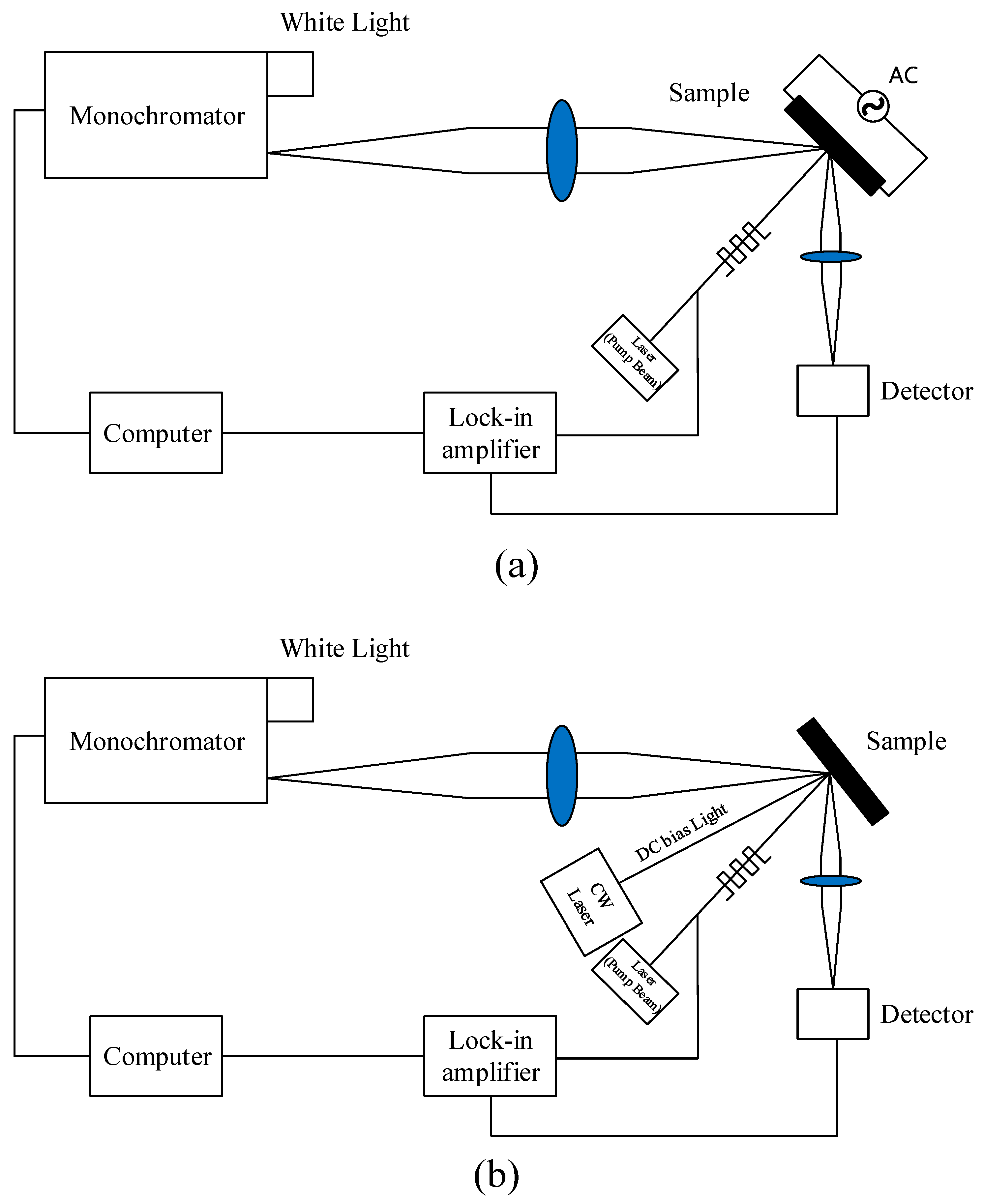
In this study, the electrical and optical biased photoreflectance (EBPR and OBPR) is used to examine the tunneling effect on the carrier density movement in this study’s dual junction solar cells. The EBPR spectrum is recorded by measuring the PR amplitude as a function of the DC bias voltage at the fixed pump beam intensity, and the OBPR spectrum is recorded by measuring the PR spectra as a function of the CW light intensity. The DC bias voltage and CW light’s internal electric field variation are measured to investigate the tunnel junction effect on the carrier density.
3. Results and Discussion
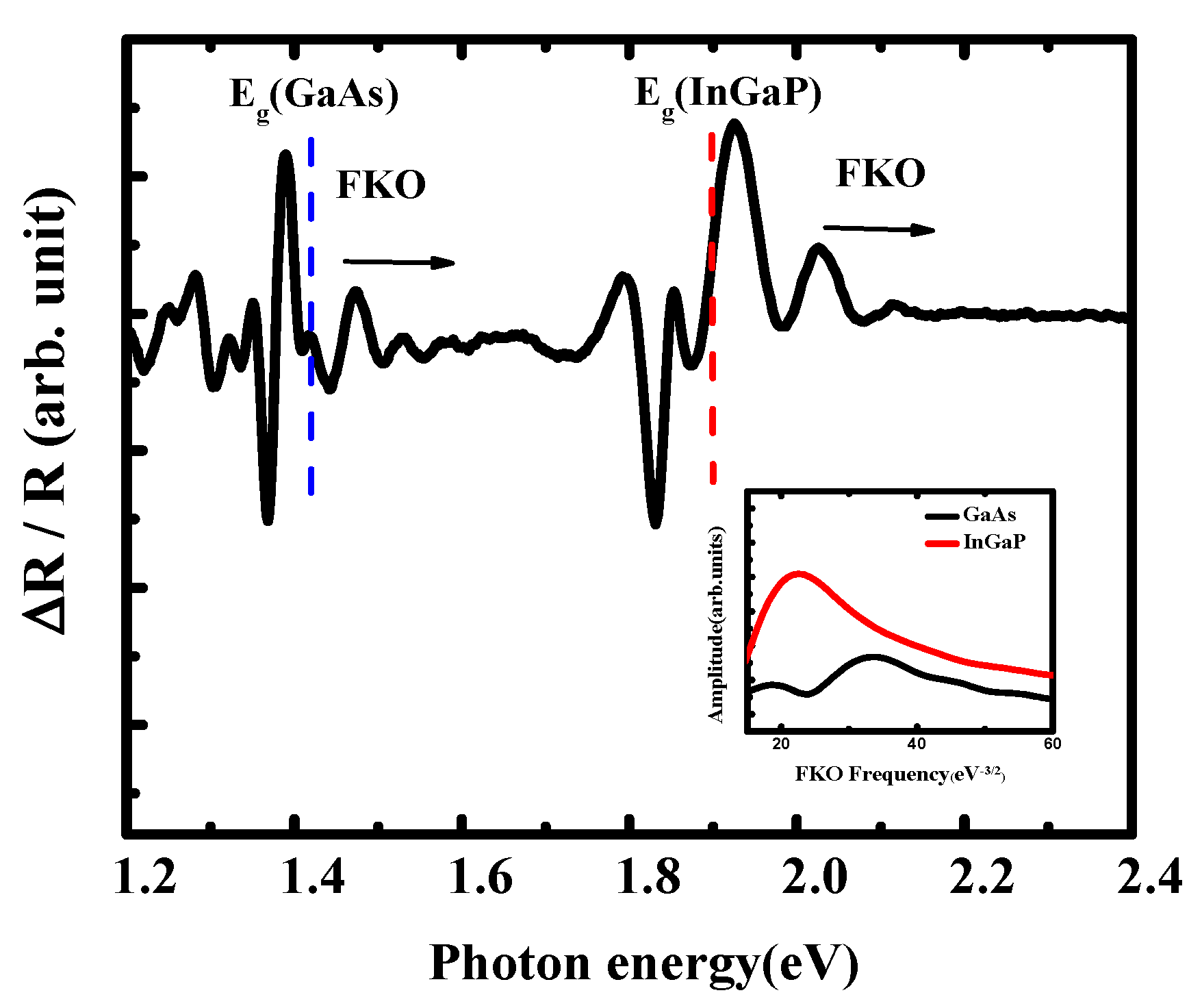
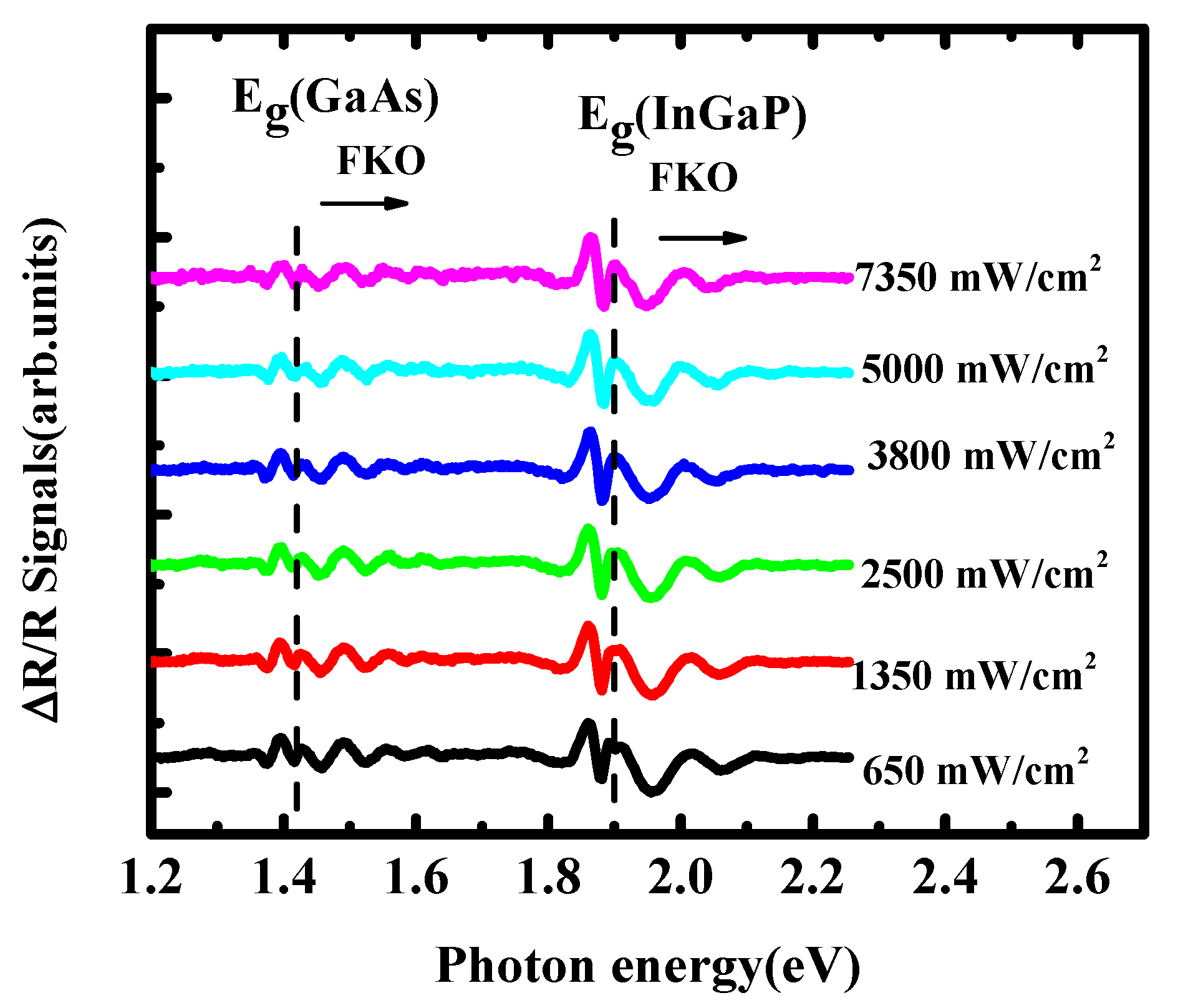
The PR spectra of the InGaP/GaAs solar cell is shown in
Figure 3. The PR spectrum contains the InGaP and GaAs band-to-band transition (E
gInGaP = 1.9 eV and E
gGaAs = 1.42 eV) and Franz—Keldysh Oscillations (FKO). At room temperature, the FKO oscillation appears in the PR spectra above the InGaP and GaAs bandgap energy because of the surface and interface electric field, as shown in
Figure 3. The Fast Fourier Transform (FFT) method was performed on the PR spectrum to recognize the FKO components in the frequency domain (eV
3/2), as shown in the inset figure.
In the high-field region, the oscillatory behavior of the FKO’s is described by Equation [
10]:
where
where the
E0 is the bandgap energy,
d is the dimensionality of the critical point,
e is the charge of an electron, ℏ is Planck’s constant,
is the frequency of FKOs and
F is the electric field strength and
µ is the reduced mass in the direction of
F. To drive the electric-field strength, estimating the oscillating period
fFFT of the FKO is done utilizing the FFT method. The period of the FKO reflects only the strength of the internal electric field as described in Equation (2), and it contains no information on its sign or direction [
11].
Generally, under illumination, the space charge field in the depletion region drifted the generated electrons and holes in opposite directions in the steady-state. These separated excess carriers induce an internal electric field in the opposite direction to the space-charge field.
Thus, the depletion region’s width and the space charge field’s strength are changed by the photogenerated induced electric field [
10]. The F
pn is affected by the carrier density variation, and the F
pn behavior is reflected in the PR spectra, especially FKO’s, because the FKO is directly associated with interface electric field strength in the sample [
12].
The PR spectra were measured using the 532 nm laser as the pump beam with energy (2.33 eV) higher than the InGaP band gap energy (1.9 eV). Therefore, the photons typically are absorbed by InGaP, and a relatively less amount of photons are transmitted and absorbed by the GaAs. Thus, the internal electric field is changed and decreased due to the photovoltaic effect. The frequency of oscillations in the FFT result is inversely related to the p-n junction’s electric field, and the values of Fpn related to the were 135.34 and 74.40 kV/cm for InGaP and GaAs, respectively.
In the multi-junction SC, the tunnel junction was a diode made of a wide bandgap and highly doped material. This decreased the depletion region length, and therefore, the electron and holes could easily tunnel through. With a tunnel-junction structure, the device’s current depends on electron transport on one side of the junction and hole transport on the other. By changing the carrier density, the internal electric field, which is an important parameter of the SC, is affected. Therefore, to investigate the SC properties and efficiency, determining the tunnel junction effect on the carrier density and internal electric field of cells is important [
12].
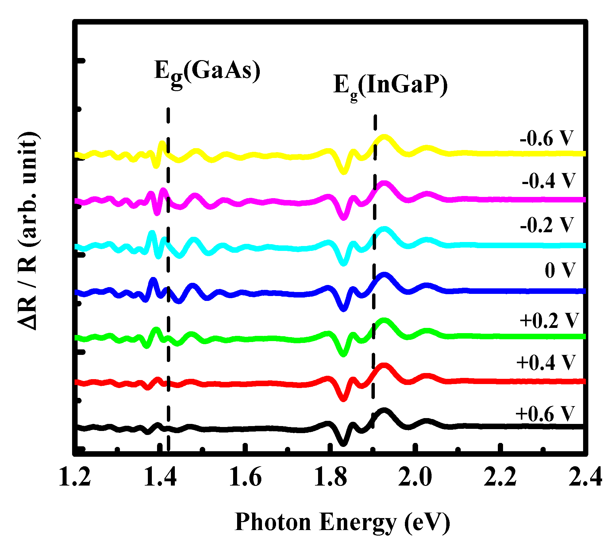
The InGaP/GaAs dual junction SC operation under a DC bias voltage was performed using DC biased photoreflectance spectroscopy (EBPR) to investigate the effect of carrier movement through tunnel junction on the electric field. The results are shown in
Figure 4.
The DC bias voltage was applied using a digital function generator, and the DC bias voltage increased from −0.6 V to +0.6 V. The PR spectra consisted of InGaP and GaAs band-to-band transition and FKO oscillations above the bandgap energies. The signals have a typical third derivate functional form (TDFF), but the amplitude of the PR signals and the Franz—Keldysh oscillations is changed when using the DC bias voltage. The shape and period of FKOs can be changed by altering the induced electric field by applying the DC bias voltage. By increasing the DC bias voltage, the peaks of the FKO shift to the left, and the period of the FKOs is decreased. The FKO components in the frequency domain are investigated using the FFT analysis on the PR spectrum. As described, the oscillation frequency is proportional to the strength of the internal electric field in the p-n junctions.
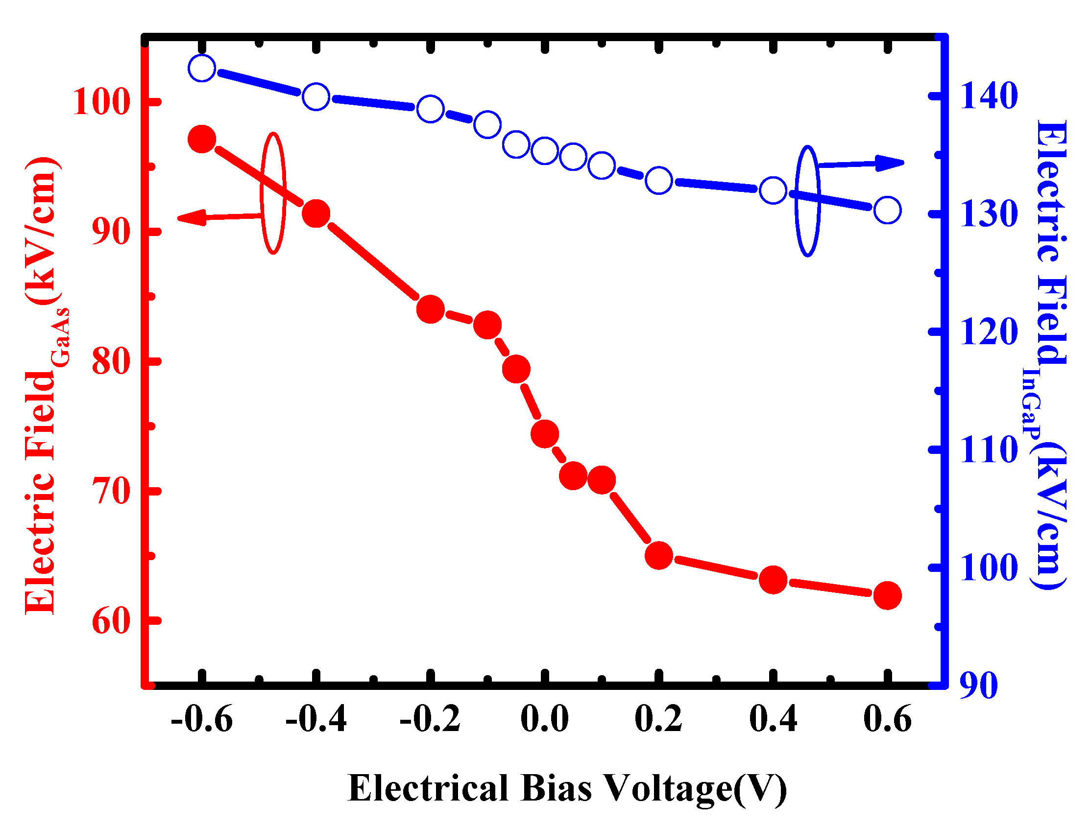
The internal electric fields are calculated using the FFT analysis, which is exhibited in
Figure 5. While the DC bias voltage was increased from −0.6 to +0.6 V, the FKO oscillations increased, and the value of F
pn reduced from 142.3 to 130.3 kV/cm and 97.1 to 62 kV/cm for InGaP and GaAs cells, respectively.
Generally, if a suitable forward bias voltage is applied to the two ends of the p-n junction, it can supply free electrons and holes with the additional energy they require to cross the junction as the width of the depletion layer around the p-n junction decreases [
13]. Decrement of the width of the depletion region and movement of the carrier to the n and p side of the junction enhanced the photogenerated induced electric field in the opposite direction of the built-in electric field. This means that the total internal electric field was reduced. Additionally, applying a reverse bias voltage results in the free charges being pulled away from the junction resulting in the increased depletion layer width. Hence, in the InGaP and GaAs cells, an increment of the voltage increased the FKO frequency. Therefore, based on the description, the internal electric field decreased and the bias voltage enhanced, owing to reducing the potential barrier of the top and bottom of cells.
Figure 5 shows the internal electrical field of InGaP and GaAs with various DC bias voltages. The results show that the decrement of the internal electric field in GaAs and InGaP is mostly due to the external bias voltage’s potential barrier variation. Furthermore, the generated carrier also affects the F
pn variation [
14].
As described previously, the pump beam is absorbed mostly by the InGaP and a few photons are absorbed by the GaAs. Therefore, the photogenerated carriers in cells affect the internal electric field strength. Resultantly, the internal electric field decreased due to the photovoltaic effect in both cells. The 532 nm laser’s input power was kept at 100 mW/cm2, and the generated carrier density was constant during the measurements. This means that the voltage variation affected the potential barrier and internal electric field strength in the EBPR measurement.
Additionally, investigating the Fpn in cells showed that the GaAs cell’s decrement rate by the DC bias voltage was higher compared to the InGaP cell. Generally, the built-in potential of the p-n structure depends on the intrinsic carrier and doping concentration. Therefore, the built-in potential in the GaAs is low. The small potential height indicates that under the same applied voltage, the variation of the potential barrier in GaAs is higher as compared to the InGaP. This indicates that due to the potential barrier’s variation, more carriers may move and drift in the p-n junction in GaAs, and the external DC bias voltage comparably decreases the internal electric field strength.
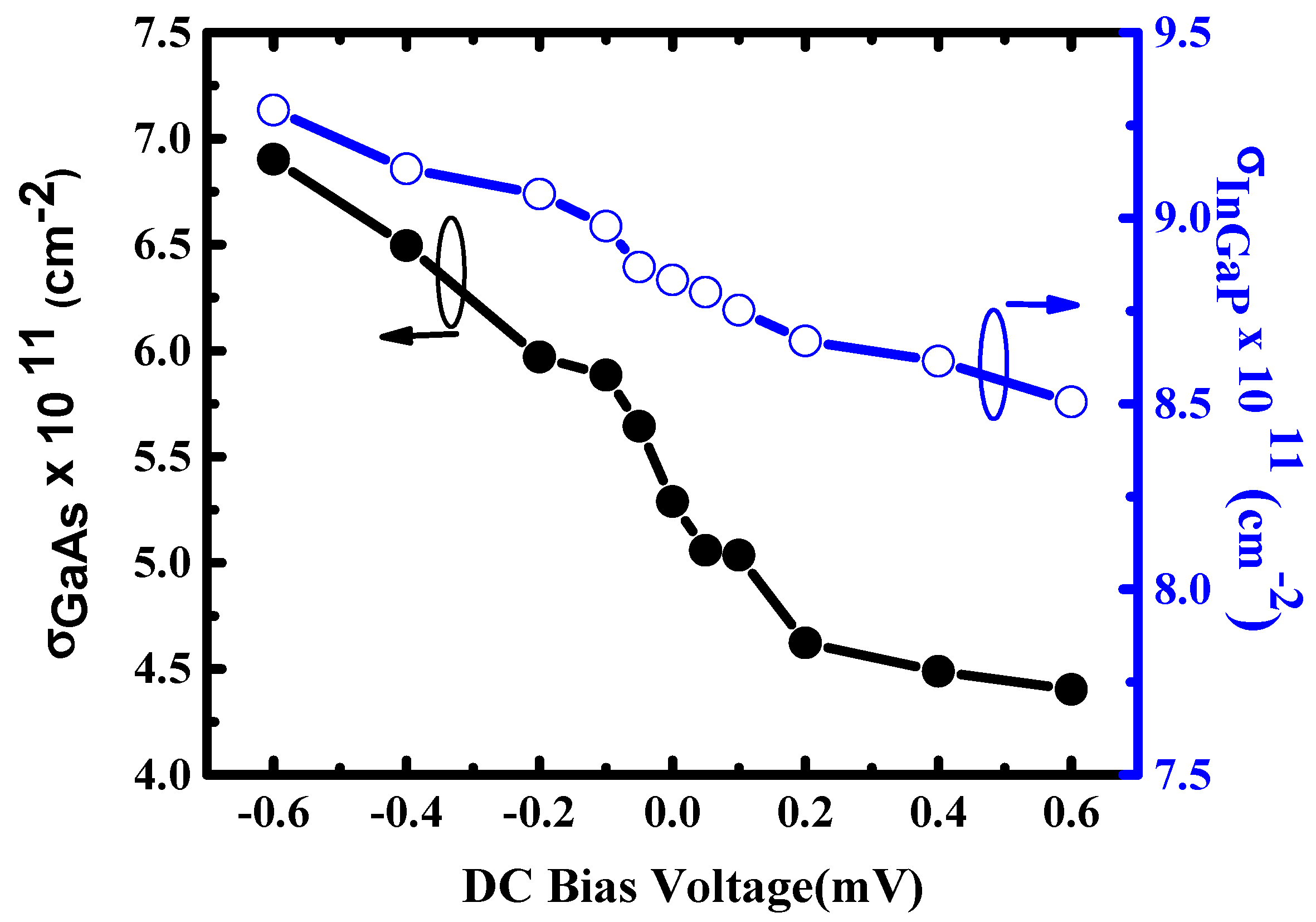
In addition, in the PR measurements, the carrier effect is not negotiable because the probe beam effect is very small. By considering the internal electric field in the p-n junctions of cells, the carrier density is caused by the electrical bias voltage, and it is represented by the following Equation [
14].
where, E is the electric field created by the bias voltage, Q is the quantity of electric charge, A is the area of the sample, ε
s is the dielectric constant of InGaP and GaAs (ε
InGaP = 11.8, ε
GaAs = 12.85), ε
0 is the permittivity of free space and σ
bi is carrier density caused by the electrical bias voltage.
Figure 6 shows the number of carrier density contribution to the photovoltaic effect. The results show that the carrier’s density, which contributes to the photovoltaic effect, in the GaAs is higher than InGaP. Meanwhile, in both cells, the carrier density number increased by increasing the reversed bias voltage.
In addition, the decrement of the internal electric field under reversed bias voltage is higher than that for the forward bias voltage. The p-n junction region acts as the electrode, and the depletion region of the p-n junction acts as the dielectric of the capacitors. Therefore, the multi-junction solar cell performs like the series capacitor. When the bias voltage is applied to the capacitor, the carriers reach the electrodes of capacitors, and a large number of charge carriers are accumulated in the electrodes [
15]. These carriers establish the electric field between two electrodes because they could not move there. The capacitance is inversely dependent on the distance between two plates and directly proportional to the electrodes’ size. Generally, in the p-n junction, two types of capacitance take place; transition and diffusion capacitance. For the reversed bias voltage, the carrier’s large number moved to the p and n side by increasing the voltage, and the depletion region width increased, whereas the size of the p and n-type region (plates) decreased. Therefore, the p-n junction with a wide depletion region and a small p and n-type region will store a small electric charge. Therefore, the reverse bias p-n junction’s capacitance decreases with voltage increment, while the potential and internal electric field variation are increased [
16].
To investigate the photogenerated carrier movement through tunnel junction effect in InGaP/GaAs dual junction SC in more detail, we measured the Optical Biased photoreflectance (OBPR) in the InGaP/GaAs dual junction solar cell. In these measurements, the 404 nm laser was used as an incident CW light source at room temperature. The power dependence of the optical CW light PR spectra is shown in
Figure 7. The CW light energy of 3.06 eV will only generate the EHP in InGaP. The pump beam with an energy of around 2.3 eV is also absorbed by cells. The carriers generated by the pump beam were located in both InGaP and GaAs. Previously we described that the InGaP mostly absorbs the pump beam, and the GaAs can absorb the small part of photons. Therefore, the carrier density generated by the pump beam in InGaP is higher than GaAs. The pump beam intensity is kept constant, and the generated carrier density can be kept constant during the measurements. At the same time, the photogenerated carriers by the CW light are located in the InGaP. Therefore, the internal electric field in the InGaP is modulated by the photogenerated carrier within the InGaP, but not the GaAs cell. Thus, the PR signal is deformed by increasing the CW light intensity in both; InGaP and GaAs. This means that the internal electric field is modulated in cells. In the multi-junction solar cell, the carriers can pass to other cells through the tunnel junction. Therefore, generated carriers by the CW beam in the top cell can pass through the tunnel junction and change the carrier’s density in the GaAs. Moreover, by changing the carrier density and modification of the internal electric field, the PR signals are changed in GaAs.
As we could see by increasing the bias light intensity (I
OB), the FKO oscillations and PR amplitude were changed. This indicated that an increase in the photogenerated carrier density decreases the interface electric fields [
12]. The photogenerated carriers create the induced electric field in the opposite direction of the built-in electric field. Therefore, with an increment of the optical bias light intensity, there will be an increase in the generated carriers, resulting in the internal electric field decrement.
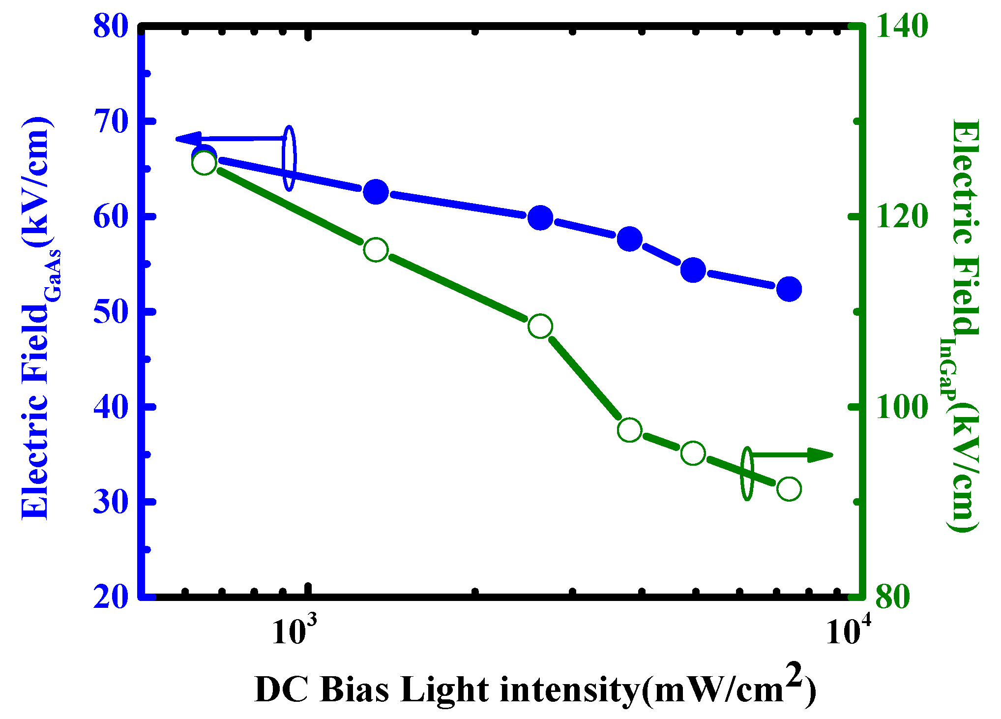
Figure 8 shows the internal electric field as a function of the CW light intensity (I
OB). F
pn is reduced in InGaP and GaAs due to the photovoltaic effect [
17].
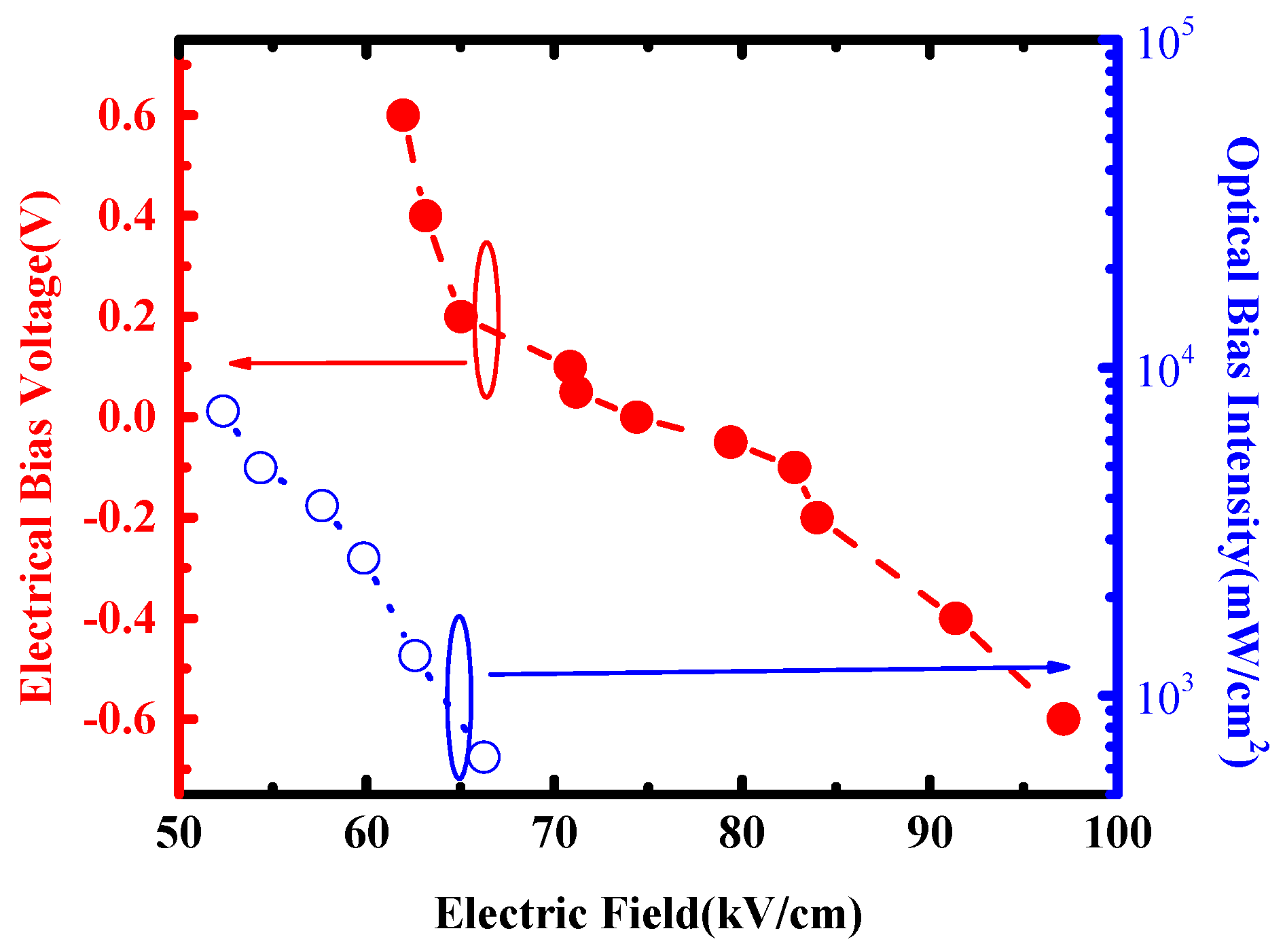
We compare the electrical bias voltage and optical bias light intensity-dependent internal electric fields of GaAs SC in
Figure 9 to examine how the tunnel junction affects carrier movement in dual junction structure. The pump beam intensity is constant, and therefore, the effect of that is the same in both measurement conditions. In electrically biased photoreflectance, the internal electric field’s decrement indicates that the decrement of the potential barrier affects internal electric fields. In these measurements, the 532 nm laser was used as an excitation source that generates the carriers in both cells, has the constant intensity during the measurements, and the carrier’s movement effect is constant. Therefore, the variation of potential affects the carrier movement and changed the internal electric field.
Figure 9 shows that F
pn strength measured under optical bias illumination is lower than F
pn measured under applying a bias voltage. The pump beam’s intensity keeps constant intensity, and therefore the photogenerated carrier density remains constant in each cell. The 404 nm laser, which is used as the CW light, has energy higher than InGaP and is mostly absorbed by it, and some part of photons can reach the GaAs. The less measured internal electric field strength under optical bias beam illumination describes that in addition to the pump beam effect, the photogenerated carrier density is also changed in GaAs cell even though the bias light has not been absorbed.
As described previously, in the PR measurement, the strength of F
pn is proportional to the period of the FKO’s, and the period of oscillation is affected by the carrier density variation. Therefore, the results show that the carrier in the GaAs is changed. In contrast, the tunnel junction exported the carrier from one cell to another cell. The photogenerated carriers by the CW light in the top cell pass through the tunnel junction. This indicates that the holes in the p- side of the InGaP pass through the tunnel junction and reach the n-side of GaAs and recombine with the electrons in the region [
18]. Changing the carrier density has an effect on the FKO oscillation period and electric field. Thus, the internal electric field in the GaAs is reduced due to the photovoltaic effect.
Therefore, understanding the carrier movement in the dual junction solar cell is important to investigate these structures’ current mismatching. In the dual junction structure, the cell which has the lowest current limits the cell current. An investigation of the carrier variation and movement by applying CW light with different energy is the method to explain the current mismatching in the dual junction solar cells. Therefore, to study the current mismatching, the photovoltaic effect was investigated by optically biased photoreflectance (OBPR) and electrically biased photoreflectance (EBPR) measurements. These spectra are sensitive to the electric field, and the Franz—Keldysh oscillation and the amplitude of the spectrum are changed.
The shape and amplitude of the spectra are changed when the CW light illuminates the SC. The internal electric fields are affected by the carrier density variation, and the variation of the internal electric field is reflected in the spectra and FKO oscillations. The internal electric field is decreased in both cells due to the photovoltaic effect. When the internal electric field changes very small under light illumination, the cell was saturated, and the number of carriers reached equilibrium and not changed more. Therefore, the current in this cell is the lowest. We can say this cell can control and limit the current in the dual junction SC. Based on the results, the internal electric field of InGaP may have the lowest changed under illuminated light. Thus, this cell can control and limit the current in the InGaP/GaAs dual junction SC. In addition to improving our result, we will use the I-V curve measurements under illuminated light with performing different wavelengths. In the future, the current mismatching will study in more detail, and we will use the optically biased ER and PR measurements.


