Article

A Multilevel Inverter Topology Using Diode Half-Bridge Circuit with Reduced Power Component

by
Jagabar Sathik
1,2,
Shady H. E. Abdel Aleem
3,
Rasoul Shalchi Alishah
4,*,
Dhafer Almakhles
1,
Kent Bertilsson
4,
Mahajan Sagar Bhaskar
1,
George Fernandez Savier
2 and
Karthikeyan Dhandapani
2
1
Renewable Energy Laboratory, Prince Sultan University, Riyadh 11586, Saudi Arabia
2
Department of Electrical and Electronics Engineering, SRM Institute of Science and Technology, Kattankulathur Campus, Kattankulathur 603203, India
3
Department of Electrical Engineering, Valley Higher Institute of Engineering and Technology, Science Valley Academy, Qalyubia 44971, Egypt
4
Department of Electronics, Mid-Sweden University, Holmgatan 10, 851 70 Sundsvall, Sweden
*
Author to whom correspondence should be addressed.
Energies 2021, 14(21), 7249; https://doi.org/10.3390/en14217249
Submission received: 13 June 2021 / Revised: 9 October 2021 / Accepted: 14 October 2021 / Published: 3 November 2021
(This article belongs to the Special Issue Power Electronics for the Grid Integration of Photovoltaic Systems)

Abstract

:
This paper presents a new multilevel converter with a reduced number of power components for medium voltage applications. Both symmetric and asymmetric structures of the presented multilevel converter are proposed. The symmetric topology requires equal dc source values, whereas the asymmetric topology uses minimum switch count. However, both structures suffer from high blocking voltage across the switches. To reduce the blocking voltage on switches, an optimal topology is presented and analyzed for the selection of the minimum number of switches and dc sources, while maintaining a low blocking voltage across the switches. A comparative analysis with recently published topologies was performed. The simulation results, as well as the comparative analysis, validated the robustness and effectiveness of the proposed topology in terms of the reduced power loss, lowered number of components, and cost. Furthermore, in addition to the simulation results, the performance of the proposed topology was verified using experimental results of 9, 17, and 25 levels.

1. Introduction

In recent years, utilization of multilevel inverters (MLIs) has increased in different applications such as renewable energy systems, utility interfacing schemes, automotive applications, and adjustable speed drives. Compared to two-level inverters, multilevel inverters offer low harmonic distortion, voltage stress on switches, and electromagnetic interference; in addition, there is no need for passive filter usage [1]. In the literature, many researchers are paying much attention to improving the structure of multilevel inverters to minimize power component number and dv/dt ratings of switches, while developing new modulation techniques to reduce the total harmonic distortion (THD) and switching losses [2,3]. The most frequently used MLIs, according to the literature, are diode clamped (dc-MLI) [4], flying capacitor (FC-MLI) [5], cascaded H-Bridge topologies (CHB-MLI) [6] and Modular Multilevel Converter (MMC) [7]. The FC-MLI topology provides better voltage balance and a more redundant state compared to the diode clamp topology. However, real power utilization is not good in FCs and a large size of dc-link capacitors is required [7,8]. Furthermore, both dc and FC topologies suffer from extra power components such as clamping diodes, dc-link capacitors. Unlike them, the CHB topology does not require any additional components or voltage balancing circuits [9]. Moreover, a cascaded connection of the two-level converter is more suitable to generate a higher number of levels and it provides enhanced modularity and reliability. Additionally, the CHB-MLI topology can be configured in both symmetric (which uses the equal magnitude of sources) and asymmetric (where the magnitudes of the dc sources are determined by geometric progression) configurations. The determination of the dc source magnitude in the case of asymmetric configurations is based on binary and trinary Algorithms [10,11,12]. Unfortunately, the CHB topology requires a large number of switches and separate dc sources. At the same time, many researchers have tried new multilevel inverter structures, while considering different criteria such as minimum number of IGBTs, dc sources, gate driver circuits, and IGBTs’ voltage rating. Several basic units and extended topologies are recommended in [13,14,15,16,17]. However, one can observe that each topology may be more suitable for specific applications, based on requirements, but may not satisfy all the design criteria at the same time. As well, the cascaded structure is introduced to reduce voltage rating on switches. The ladder structure of bidirectional switches is used for series connection of non-isolated dc sources, and it was observed that as the number of levels goes high, the blocking voltage on the bidirectional switches increases, and most of the switches are in different voltage ratings in symmetric methods [18,19,20,21]. In [22], a series-connected half-bridge structure is used to produce multilevel dc/dc voltage waveforms. A high number of IGBTs was required because unidirectional switches are used. In [23,24,25,26,27,28,29,30,31,32,33], the bidirectional switches are replaced with a diode and series-connected unidirectional IGBTs. In [23,24,25], the topologies are proposed with cascaded structure and optimal topology to determine the minimum number of power components against the number of voltage levels. However, the number of power electronics components and blocking voltage on switches is increasing. Further, topologies [26,27,28,29,30,31,32,33] have recently been published and these topologies are generating a higher number of voltage levels, but the stress on the switch, the number of power components, and dc sources are increasing as the number of levels increases. The modular multilevel converter (MMC) [34,35,36,37] is quite famous for high voltage applications. However, this NPC MLI and MMC circuit needs separate control techniques to balance the capacitors, and also the number of device counts is high [36,38]. It was observed that the presented topology required a low number of IGBTs.
From the above discussion, most of the MLI topologies required a higher number of switches, gate driver circuits and heat sink modules which are further directly involved in the cost and size of the inverter. In order to reduce the switches and required number of dc sources, in this paper, new symmetric and asymmetric multilevel converter topologies are proposed with a reduced number of switches and power components (dc sources, IGBTs, and driver circuits), while maintaining acceptable blocking voltage values. The proposed multilevel inverter is configured in symmetric, asymmetric, and cascaded methods by connecting a k-unit of the sub-multilevel inverter. A comparative analysis of the proposed topologies and other recently published topologies is presented, and the advantages of the proposed topologies are as follows:
(1)
The number of switches is reduced, which further reduces the number of driver circuits and heat sinks.
(2)
Due to the reduction of the number of switches, the power loss is minimized.
(3)
The number of isolated dc sources is reduced.
The cost of the inverter is reduced, and efficiency is increased. The proposed topologies are more suitable for medium voltage applications due to blocking voltage considerations. The paper is organized as follows: Section 2 presents the basic module of the proposed topology and the switching sequence. Additionally, in Section 2, an extended topology of the basic module is proposed and discussed for the symmetric configuration. The asymmetric configuration is proposed in Section 2. A comparison of both symmetric and asymmetric configurations is shown. Drawbacks of both configurations are highlighted. In Section 3, a cascaded topology is recommended, and two different Algorithms are presented to determine the magnitudes of the dc sources. The proposed topology is optimized for different goals and compared with recent topologies in Section 4. The comparison with recent topologies is given in Section 5. In Section 6, the modulation scheme is presented. The experimental test results are presented and discussed in Section 7. Finally, conclusions are given in Section 8.

2. Proposed Multilevel Inverter Topology

The basic module is shown in Figure 1, and it consists of two dc-link capacitors (C1 and C2), two diodes (D1 and D2), and two IGBTs (Sx and Sy). It produces output voltage levels as +Vdc and 2Vdc as shown in Table 1. When the diode D1 is conducted and Sy is turned on, Vdc will be produced. Further, 2Vdc will be produced when both Sx and Sy are turned on. The D2 is used to avoid short-circuiting of the source. By using this proposed basic module, three different topologies, named Symmetric Diode Half-Bridge Multilevel Inverter, Asymmetric Diode Half-Bridge Multilevel Inverter, and Cascaded Asymmetric Diode Half-Bridge Multilevel Inverter, can be introduced.

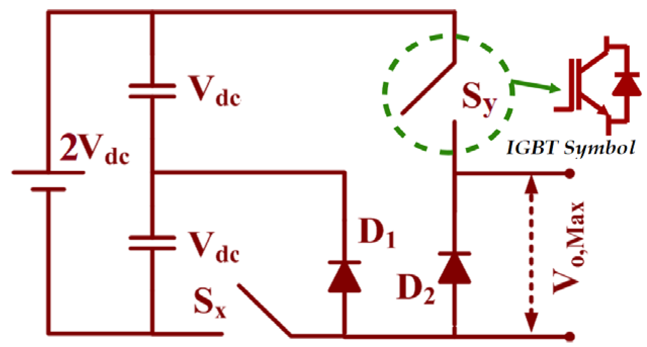
2.1. Symmetric Diode Half-Bridge (SDHB) Multilevel Inverter Topology

A generalized structure of the proposed multilevel inverter of the symmetric configuration is shown in Figure 2. It consists of n − 1 basic module and the nth module has one IGBT and one diode. In the symmetric configuration, the dc sources are equal as given in (1). By using (2), the corresponding maximum output voltage (Vo,max) can be obtained.
V 1 = V 2 = V 3 = .... = V n = V d c
V o , max = 2 n V d c
The switching sequence and corresponding states are given in Table 2 to synthesize the multiple stepped dc output voltage waveforms. The full-bridge inverter at the load side produces the positive and negative output voltage levels such as ±Vdc, ±2Vdc up to ±nVdc. The required number of switches (NIGBTs), diodes (Ndiode), and the dc-link capacitors (Ncapacitor) are obtained, respectively, as expressed in (3) and (4), where n represents the number of modules.
N L e v e l = 4 n + 1 ,   N I G B T s = 2 n + 3
N C a p a c i t o r = 2 n ,   N d i o d e = 2 n 1

2.2. Asymmetric Diode Half-Bridge (ADHB) Multilevel Inverter Topology

The symmetric topology is more suitable when the values of the dc sources are equal; but the required number of power components like switches, dc sources, and gate driver circuits will increase in proportional to the number of voltage levels. This is an obvious disadvantage with a large number of voltage levels. On the other side, the asymmetric topology requires low numbers of components compared with the symmetric topology. The structure of the ADHB is given in Figure 3 and the switching sequence is given in Table 3. The ADHB topology consists of n number of basic modules connected in series, in addition to the full-bridge inverter on the load side. Similar to the conventional CHB topology, the proposed asymmetric method is also configured in trinary configuration, and determination of the magnitude of the dc voltage sources and the maximum output voltage, is expressed as follows,
V 1 = V d c , V 2 = 3 V d c , .... V n = 3 n 1 V d c
V o , m a x = [ ( 2 × 3 n ) 2 2 ] V d c
For this topology, numbers of the output voltage levels and IGBTs are given in (7) and (8), respectively.
N L e v e l = ( 2 × 3 n ) 1
N I G B T s = 2 n + 4
The comparison of the symmetric and asymmetric DHB topologies, in addition to the topologies presented in [13,14,15,16,17], is shown in Figure 4.
As obvious, the proposed topologies require a lower number of power components compared to the conventional topologies. Moreover, in the proposed topologies, the required number of isolated dc sources is lower than that required in the other topologies. This makes it more suitable for renewable energy source applications, especially photovoltaic systems. However, a remarkable disadvantage is that these topologies suffer from high voltage stresses on the full-bridge inverters switches because of dc voltage sum across the switches (F11F14). Consequently, the proposed topologies are more suitable for medium voltage applications. In addition, the series connection of the dc-link capacitors results in a non-equal share of the voltages. Thus, an extra circuit that has one capacitor and three diodes as provided in [23] will be required to stabilize the voltage across the capacitors.

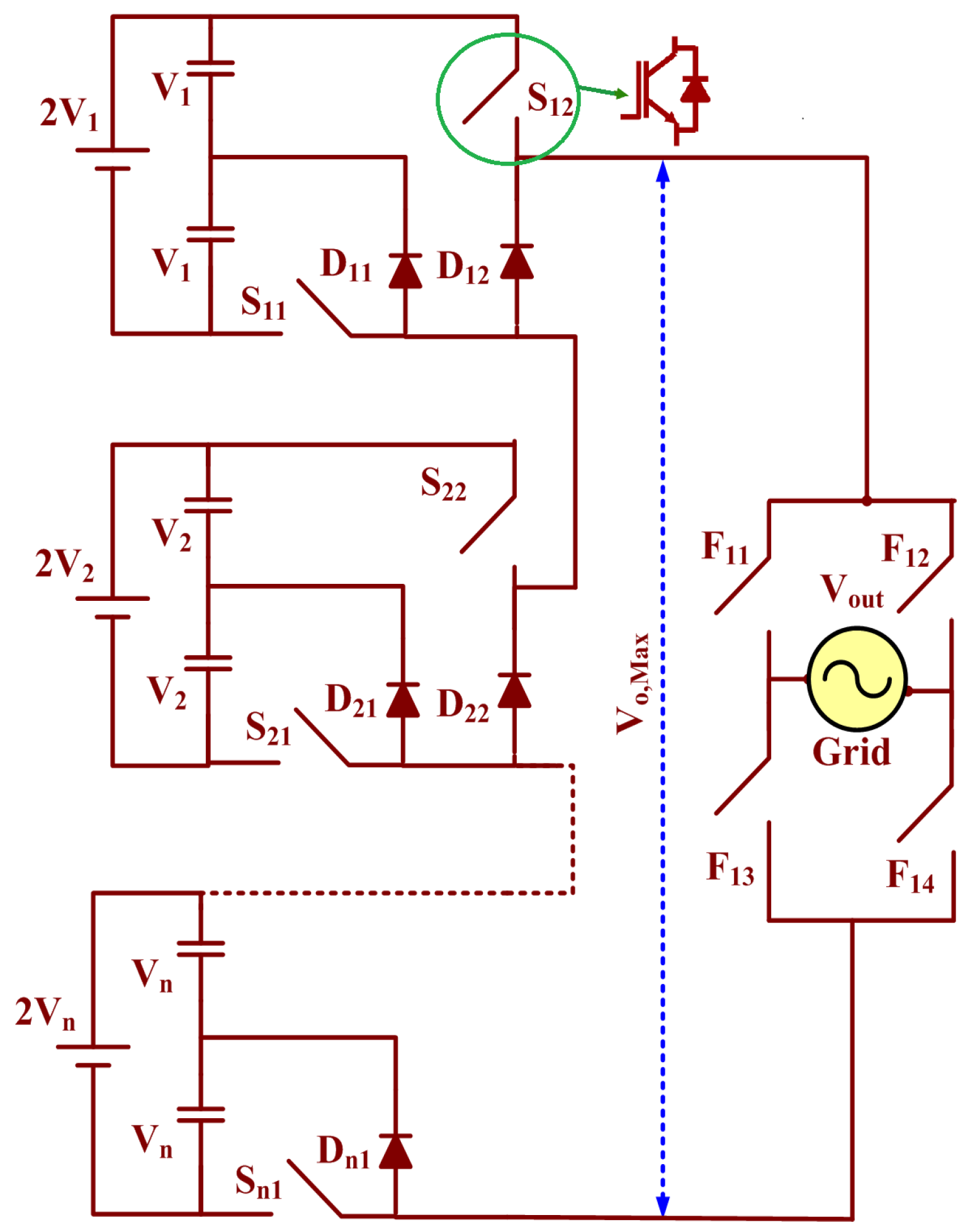
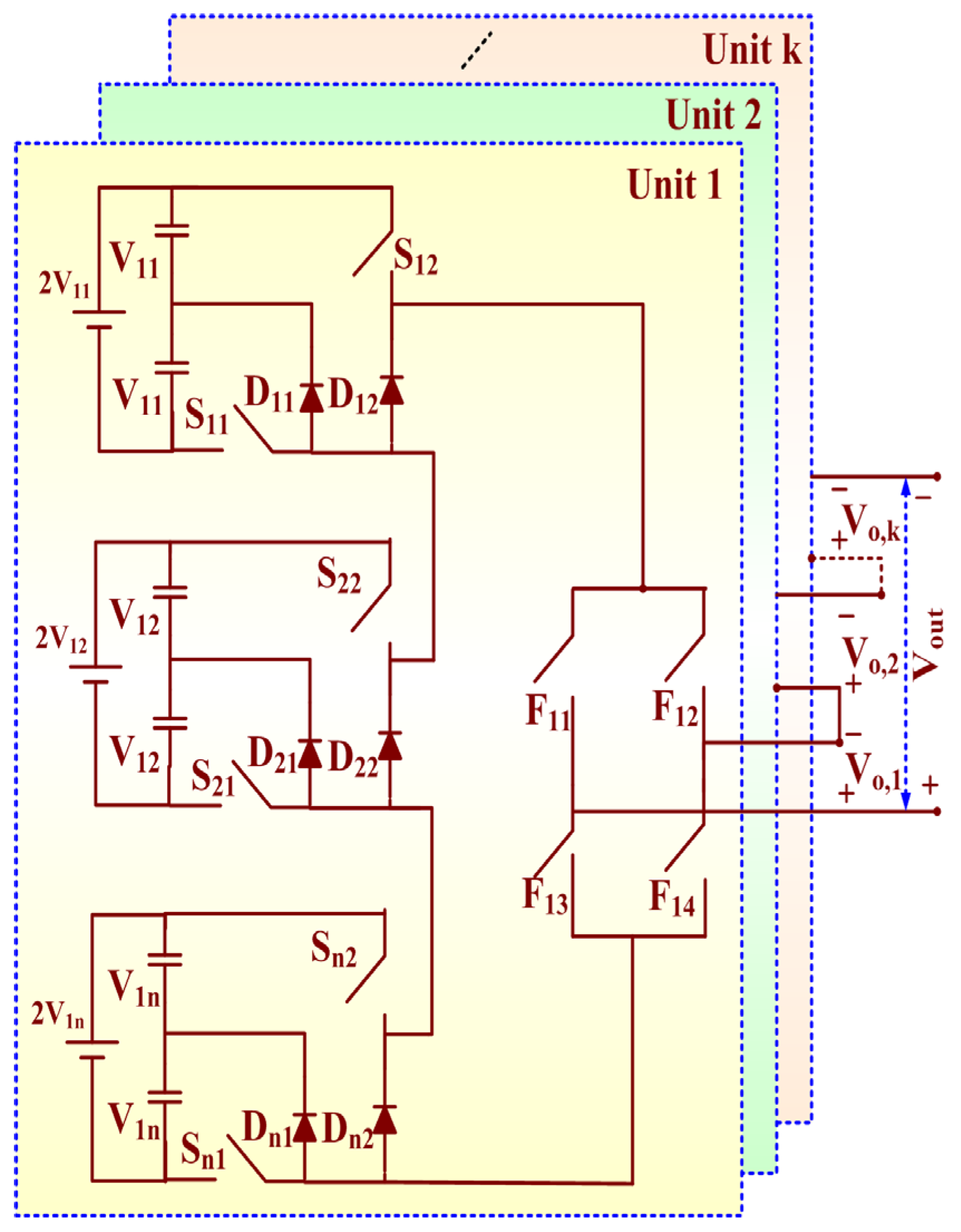
3. Cascaded Asymmetric Diode Half-Bridge Multilevel Converter

The symmetric and asymmetric configurations suffer from high blocking voltage across the switches, which necessitate the design of the full-bridge switches to withstand the sum of all the dc source values as well as the increase of the ratings of the gate driver and snubber circuits and using cooling schemes (which increase the cost of inverters). Hence, to avoid such problems, a cascaded topology is recommended for a higher number of levels with reduced maximum blocking voltage across the switches. However, the uneven power distribution is occurred in asymmetric topologies due to the number of switching of few switches are higher than other switches. This is even occurring in conventional CHB topology asymmetric configuration and this is a remarkable drawback of asymmetric configuration.
A cascaded diode half-bridge configuration consists of k units, and each unit has 2n number of capacitors and diodes. Each unit is named as a sub-multilevel inverter (SMLI) with n modules so that each SMLI has an equal number of modules as given in Figure 5. Each SMLI produces Vo,1, Vo,2Vo,k, so that the output voltage (Vout) equals the kth voltage sum. A high number of levels can be achieved by the determination of magnitudes of the dc sources. In this work, two possible algorithms are proposed to determine the magnitudes of the dc sources.

3.1. The First Algorithm

In the first algorithm, all the dc source values are equal. For each SMLI, the determination of the magnitudes of the dc sources is given as follows.
For 1st SMLI:
V 11 = V 12 = V 13 = .... = V 1 n = V d c
V o 1 , m a x = [ ( 4 n + 1 ) 1 2 ] = 2 n V d c
The number of output voltage levels generated by the first SMLI is given as follows,
N L e v e l , 1 = 4 n + 1
2nd SMLI:
V 21 = 2 ( V o , 1 max ) + V d c
V 21 = V 22 = V 23 = .... = V 2 n = ( 4 n + 1 ) V d c
V o 1 , m a x = 2 n ( 4 n + 1 ) V d c
The numbers of output voltage levels generated by the first and second SMLIs are obtained as follows,
N L e v e l , 2 = ( 4 n + 1 ) 2
kth SMLI:
V k 1 = V k 2 = V k 3 = .... = V k n = ( 4 n + 1 ) k 1 V d c
V o k , m a x = 2 n ( 4 n + 1 ) k 1 V d c
The maximum output voltage and number of output voltage levels based on the first algorithm are expressed as follows,
V o , m a x = ( N L e v e l 1 2 ) V d c
N L e v e l , k = ( 4 n + 1 ) k

3.2. The Second Algorithm

In the second algorithm, all the dc source values are unequal, i.e., each SMLI has a trinary geometric progression of dc source magnitudes. The dc source values of each SMLI are determined as follows,
1st SMLI:
V 11 = V d c , V 12 = 3 V d c , V 13 = 9 V d c , V 1 n = 3 n 1 V d c
V o , 1 , max = ( 1 + 3 + 9 + + 3 n ) V d c = ( i = 1 n V 1 i ) V d c
2nd SMLI:
V 21 = 2 ( 2 V 11 + 2 V 12 ... + 2 V 1 n ) + V d c = [ 2 ( 3 n ) 1 ] V d c  
V 22 = 3 V 21 , V 23 = 3 2 V 22 ... V 2 n = [ 2 ( 3 n ) 1 ] ( 3 n - 1 ) V d c
V o , 2 , max = i = 1 n V 2 i = i = 1 n [ [ 2 ( 3 i ) 1 ] × ( 3 i 1 ) 1 2 ] V d c
kth SMLI:
V k n = [ 2 ( 3 n ) k 1 × ( 3 n 1 ) ] V d c  
V o , k , max = i = 1 n V k i = i = 1 n ( [ 2 ( 3 i ) 1 ] k 1 × ( 3 i 1 ) 1 ) 2 V d c
The maximum output voltage and number of output voltage levels based on the second algorithm are expressed as follows,
V o , max = ( N L e v e l 1 2 ) V d c
N L e v e l , k = [ 2 ( 3 n ) 1 ] k
Numbers of IGBT, drivers, diodes and dc-link capacitors are given by,
N I G B T s = N d r i v e r = ( 2 n + 4 ) k
N C a p a c i t o r = N d i o d e = 2 n k

3.3. Total Blocking Voltage

The voltage and current ratings of the switches is an important factor that decides the cost of an inverter. In general, all the switches carry the same current with respect to the load. However, this is not true for voltages, as switches withstand different voltages based on the topology structure. In this work, a total blocking voltage (TBlock) represents the sum of the maximum blocking voltage of all the switches. It is expressed as follows,
T B l o c k = V T , M o d u l e + V F B
where VT,Module and VFB represent the total blocking voltage of the switches in a module and full-bridge, respectively. VT,Module is expressed as follows,
V T , M o d u l e = 3 2 ( j = 1 n i = 1 n V i , j ) V d c = ( 3 ( N L e v e l 1 ) 4 ) V d c
Additionally, VFB is given by,
V F B = 4 ( j = 1 n i = 1 n V i , j ) = 2 ( N L e v e l 1 ) V d c
Hence, by summing (32) and (33), one can express TBlock of the switches of the proposed topologies as follows,
T B l o c k = ( 11 ( N L e v e l 1 ) 4 ) V d c

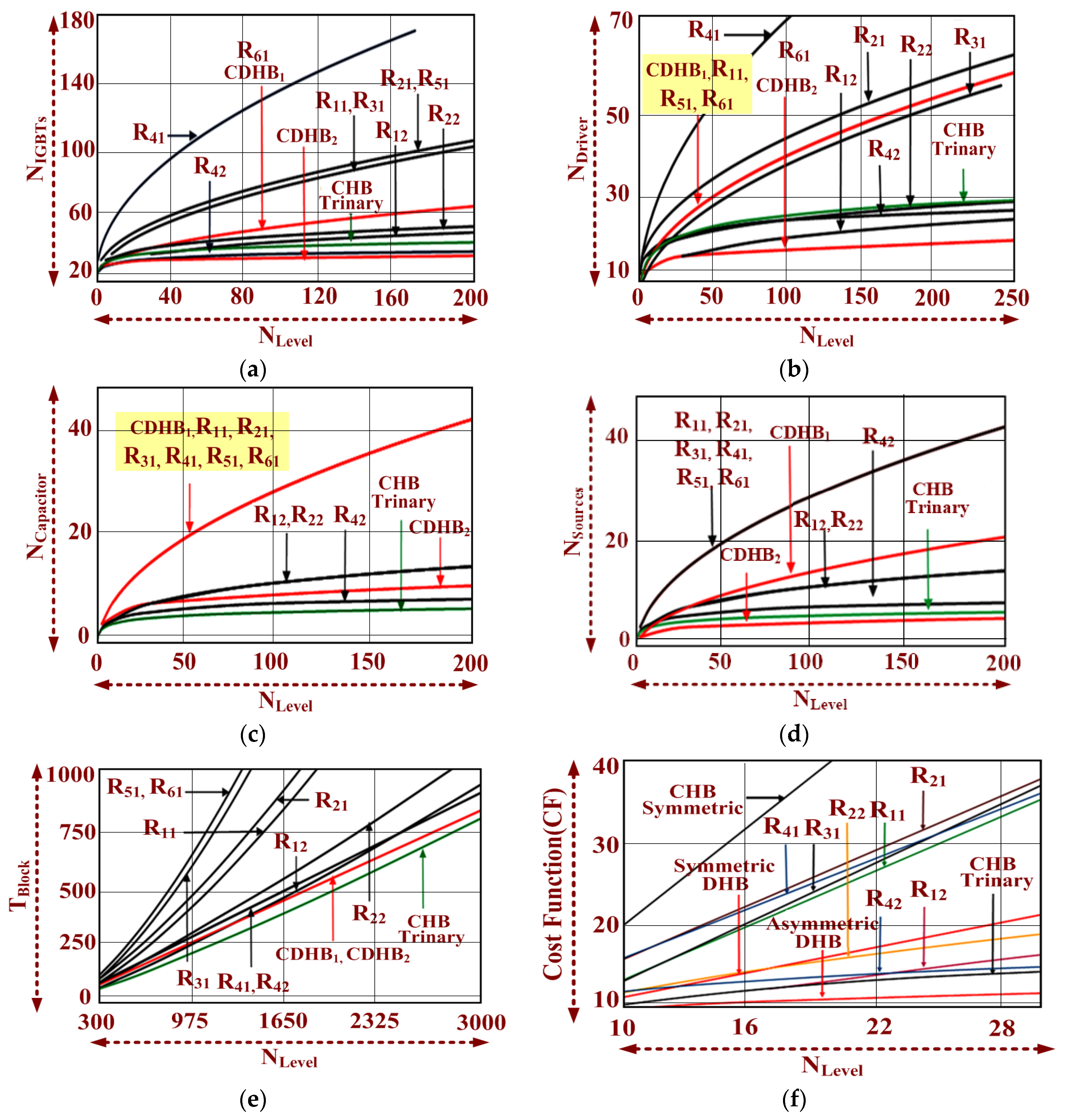
4. Optimal Topology of the Proposed Multilevel Converter

In this section, a comparative study of the results of various topologies given in [18,19,20,21,22,23] is presented to show the advantages of the proposed topology. In the comparative study, R11 denotes the topology of the first algorithm, while R12 denotes the topology of the second algorithm presented in [18], R21 and R22 denote the same but for the algorithms presented in [19]. Like so, R31 denotes the topology in [20], R41 and R42 denote the topologies of Algorithms 1 and 3 in [21], R15 denotes the topology in [22], R16 denotes the topology in [23], and CDHB1 denotes the proposed topology based on the first algorithm, while CDHB2 denotes the proposed topology based on the second algorithm.
The comparative analysis is presented in Figure 6 and Figure 7 in terms of a number of components such as NIGBT, Ndiode, Nsource, Ncapacitor, and Ndriver, as well as TBlock.

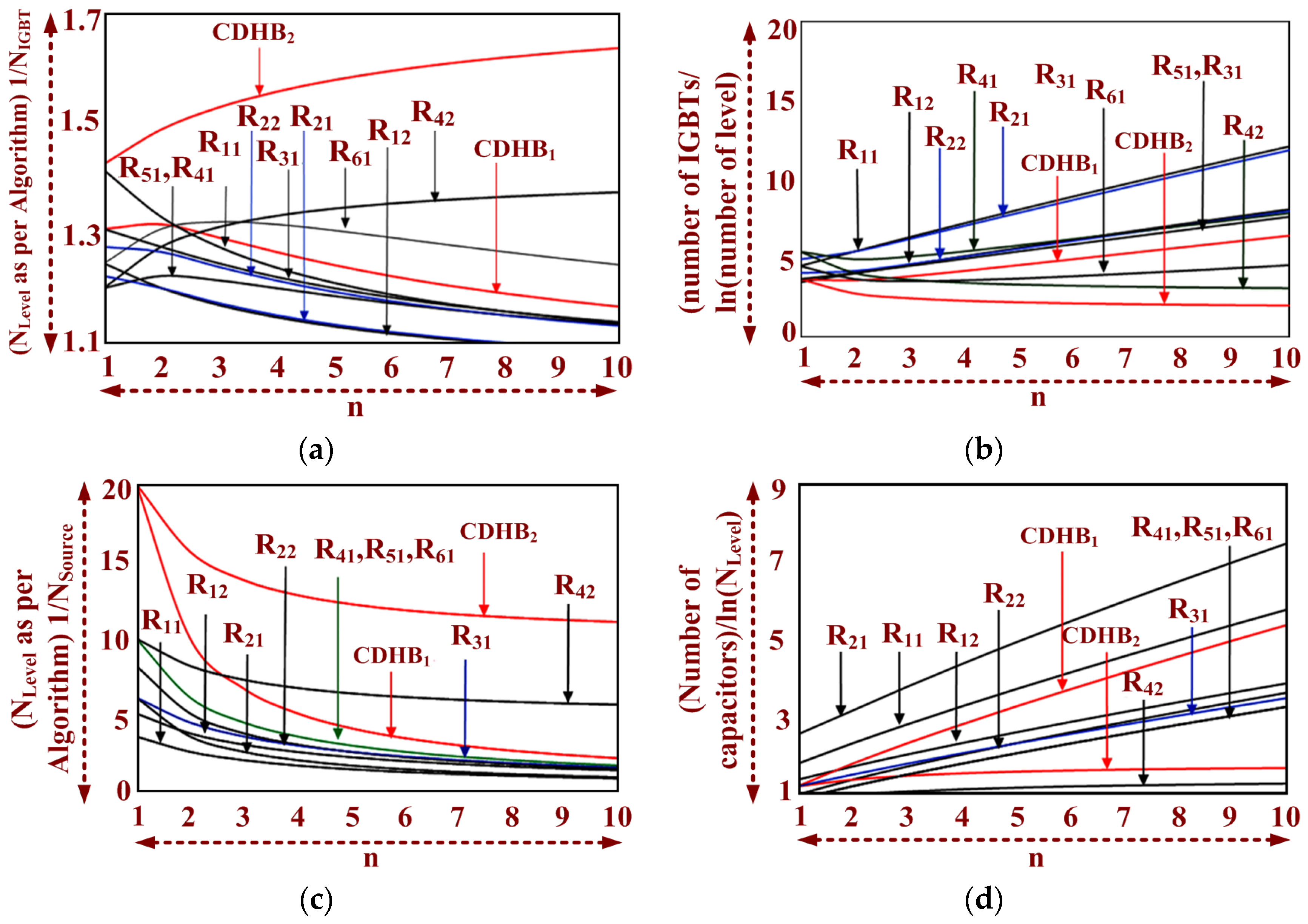
4.1. Number of Voltage Levels with a Constant Number of IGBTs

Considering the constant number of switches is kept in each unit. Thus,
N I G B T s = ( 2 n 1 + 4 ) = ( 2 n 2 + 4 ) = ( 2 n k + 4 ) k = N I G B T s / 2 n + 4 , ( when   n 1 = n 2 = ... = n k )
Hence, numbers of voltage levels of the first and second algorithms are determined with a constant number of IGBTs as follows,
N L e v e l , 1 = [ ( 4 n + 1 ) 1 / ( 2 n + 4 ) ] N I G B T
N L e v e l , 2 = [ ( 2 ( 3 n 1 ) ) 1 / ( 2 n + 4 ) ] N I G B T
Figure 6a shows that CDHB2 gives the maximum number of output voltage levels, when n > 1, compared to the other topologies.

4.2. Number of IGBTs with a Constant Number of Voltage Levels

The number of IGBTs of the first and second algorithms is determined with a constant number of voltage levels, respectively, as follows,
N I G B T s = ln ( N L e v e l , 1 ) ( ( 2 n + 4 ) ln ( 4 n + 1 ) )
N I G B T s = ln ( N L e v e l , 2 ) ( ( 2 n + 4 ) ln ( 2 ( 3 n 1 ) ) )
Figure 6b shows that the proposed cascaded structure gives the minimum number of IGBTs when n = 1. When n > 1, the required number of IGBTs are increasing for the topologies presented in [18,19,20,21,22,23] and CDHB1; but is decreasing gradually with the increase of levels for the proposed CDHB2.

4.3. Number of Voltage Levels with a Constant Number of Sources

Recalling Figure 5, the number of sources required for each unit is given as Nsource = n1 + n2 + n3 + … + nk, thus for the kth unit, it is given as Nsource = nk. Hence, numbers of voltage levels of the first and second algorithms are determined with a constant number of sources as follows,
N L e v e l , 1 = [ ( 4 n + 1 ) 1 / n ] N s o u r c e s
N L e v e l , 2 = [ ( 2 ( 3 n 1 ) ) 1 / n ] N s o u r c e s
Figure 6c shows that the proposed cascaded structure gives the minimum number of sources and produces the maximum number of output voltage levels compared to the other considered structures, especially with n = 1.

4.4. Number of Capacitors with a Constant Number of Voltage Levels

The number of capacitors of the first and second algorithms is determined with a constant number of voltage levels, respectively, as follows,
N C a p a c i t o r s = ln ( N L e v e l ) ( 2 n ln ( 4 n + 1 ) )
N C a p a c i t o r s = ln ( N L e v e l ) ( 2 n ln ( 2 ( 3 n 1 ) ) )
As shown in Figure 6d, it is clear that all the topologies require a minimum number of capacitors when n = 1. Additionally, the required number of power components is high in first algorithm as compared to the second algorithm to generate the same stepped voltage level.

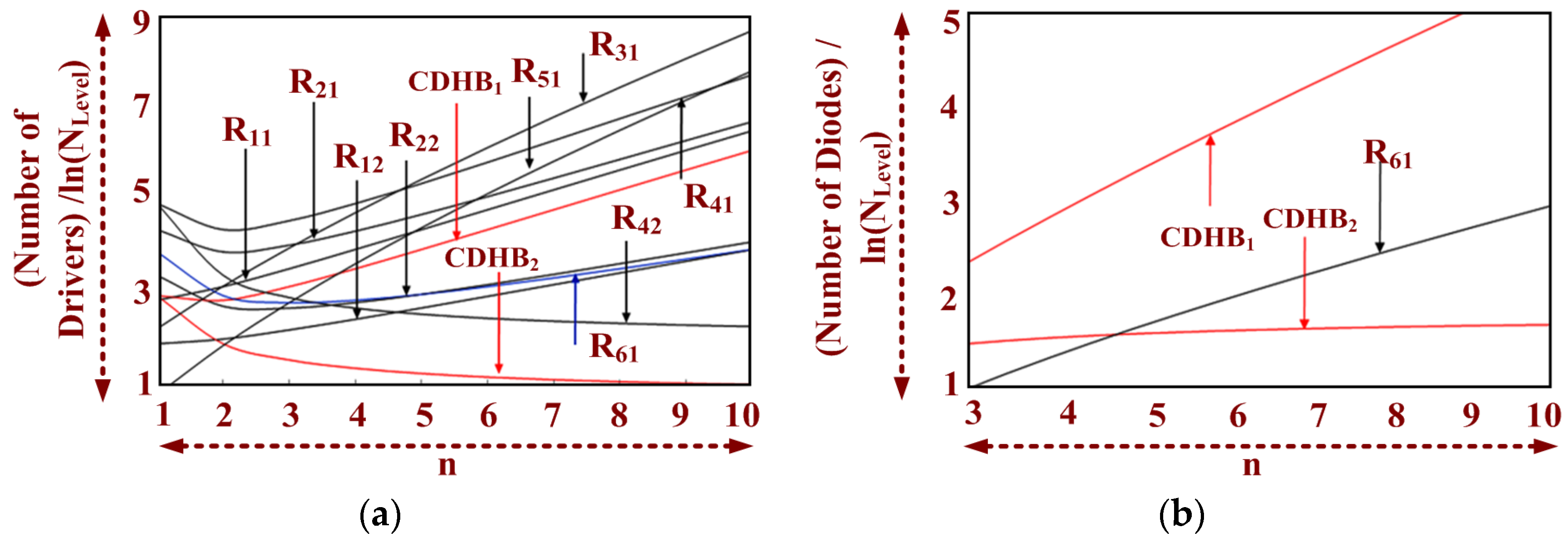
4.5. Number of Drivers with a Constant Number of Voltage Levels

The driver circuits are related to the cost and reliability of the inverter directly. The presented topologies in [18,19,20] have used bidirectional switches which require single driver circuits to turn the two switches. As shown in Figure 7a, CDHB2 uses a fewer number of driver circuits compared to the other topologies. Furthermore, an equal number is required of the IGBTs and driver circuits for the proposed topologies. Therefore, Equations (38) and (39) express also the number of driver circuits of CDHB1 and CDHB2, respectively.

4.6. Number of Diodes with a Constant Number of Voltage Levels

The lifetime of diodes is higher than other power electronic components. Each module of the proposed topology uses two diodes. Thus, the minimum numbers of diodes for a constant number of voltage levels are given for CDHB1 and CDHB2 as follows,
N d i o d e = ln ( N L e v e l ) ( 2 n ln ( 4 n + 1 ) )
N d i o d e = ln ( N L e v e l ) ( 2 n ln ( 2 ( 3 n 1 ) ) )
Figure 7b shows that the proposed CDHB topology requires a minimum number of diodes compared to the topology in [23]. Additionally, the second algorithm is better than the first algorithm and the topology in [23], especially with the increase of n. For diode count, the IGBTs parallel didoes are not considered.

4.7. Blocking Voltage Rating with a Constant Number of Voltage Levels

As the blocking voltage increases, the voltage rating of IGBTs and supporting components (snubber circuit, heat sink, and cooling system) increase. To identify the minimum blocking voltage of the proposed topologies, a constant number of levels are considered, and it was found that the switches require minimum blocking voltage when NLevel is low, i.e., n = 1.

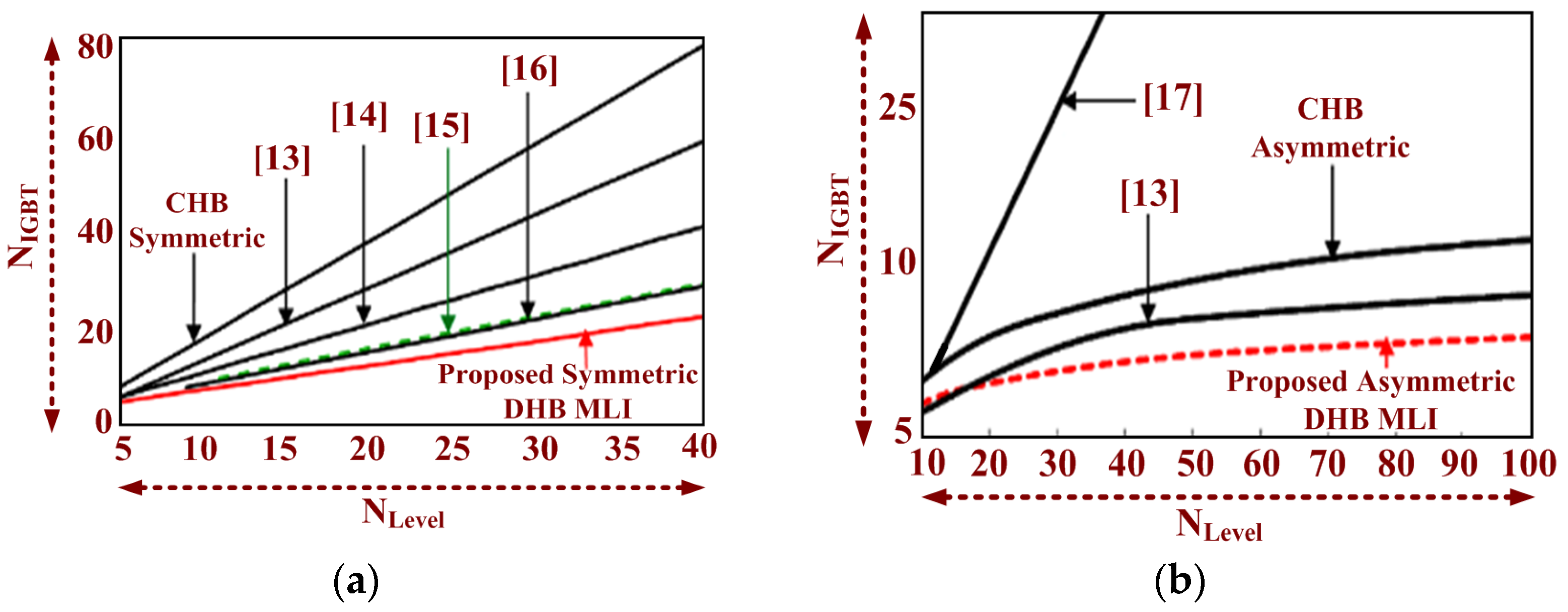
5. Comparative Study with Recent Cascaded Multilevel Inverter Topologies

The cascaded DHB topology is compared with recent cascaded multilevel inverter topologies presented in [18,19,20,21,22,23] to show its advantages as shown in Figure 8. In this comparative analysis, all the topologies were considered for k = 2.

5.1. The Required Number of IGBTs against the Number of Levels

The increased number of IGBTs results in using extra components such as anti-parallel diodes, heat sinks, cables, layouts, and digital logic gates to generate the switching pattern. It is observable from Figure 8a that the proposed topology based on the two suggested algorithms produces the maximum number of levels with a lower number of IGBTs compared to the trinary configuration of the conventional cascaded topology and the other considered topologies.

5.2. The Required Number of Driver Circuits against the Number of Levels

The driver circuits and some associated components such as optocouplers are usually taken into account to measure the performance of a multilevel inverter. An increasing number of driver circuits degrades the reliability of the multilevel inverter and leads to a further increase of the complex switching control. As presented in Figure 8b, the proposed cascaded topology using the second algorithm requires fewer driver circuits than the other topologies.

5.3. The Required Number of Dc Sources/Capacitors Number of Levels

For the n module, the proposed structure requires a 2n number of dc-link capacitors while the other topologies use one dc-link capacitor but with a higher peak magnitude. Figure 8c shows the graph of the number of capacitors versus the number of levels. The proposed topology offers a reduction of the size and cost of the dc-link capacitors. However, it should be mentioned that series connection of the dc-link capacitors requires balancing circuits. As shown in Figure 8d, dc sources varieties are equal in all the topologies and CDHB1. However, CDHB2 requires n varieties dc sources.

5.4. Total Blocking Voltage against the Number of Levels

For all the considered cases, the cascaded trinary configuration and the proposed cascaded structure introduce the lowest total blocking voltage compared to the other topologies particularly with a high number of levels, as shown in Figure 8e. The topology presented in [24] needs a higher number of IGBTs and Maximum blocking voltage on the switch.

5.5. Cost

The multilevel inverter cost is a good index to decide the topology’s effectiveness from a customer viewpoint. The cost depends on the number and rating (voltage and current) of the power components, as well as the number of driver circuits and dc sources [20]. Recalling that the proposed topology uses a fewer number of IGBTs, driver circuits with low total blocking voltage; accordingly, the cost of the proposed inverter is lower than the other topologies. Furthermore, the cost of the switches increases by the increase of the current rating of the switches. In this work, the current rating of switches is determined by factor α. For the same voltage rating, increasing α will increase the MLI cost. Figure 8f shows a comparison of the proposed symmetric and asymmetric topologies and the other considered topologies at α = 0.5. In this comparison, the driver circuits and dc sources are not included. It is clearly obvious that the cost of the asymmetric topology (CDHB2) is considerably less than the other topologies. Further, in Table 4, recent multilevel inverter topologies [27,28,29,30] are compared with the proposed topology. However, the front-end converter is not considered for the cost comparison because the front-end converter is most required and common to all the topologies for voltage regulation. For example, the conventional CHB topology needs two sets of voltage regulations to generate a five-level stepped voltage waveform likewise other topologies also require the front-end regulation circuits. It is here worth mentioning that the required number of front end dc/dc converters depends on the dc source, so, the proposed topology required two dc sources to generate the 25 L as compared to other topologies.

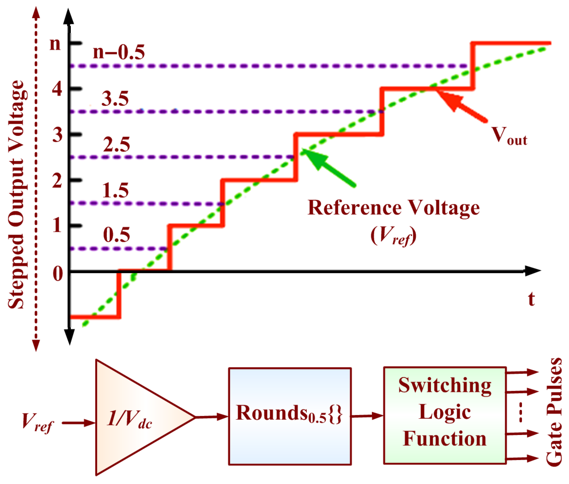
6. Nearest Level Modulation Technique

The nearest level modulation technique operates in fundamental switching frequency and produces low THD at a higher number of voltage levels [12]. The NLC method {x} is rounded to the nearest integer value, where x represents the reference value and the comparing value is half-integer value 0.5, i.e., round (1.6) = 2 and round (1.4) = 1). The half-integer always rounded off to the real integers. Figure 9 shows the simulation output voltage and current waveforms. Figure 10 shows the schematic pulse generation using the NLC method. In conventional NLC the output voltage error is 0.5 Vdc whereas in proposed NLC the output voltage error is minimized to 0.4 Vdc as given in Equation (46) and the output voltage RMS is higher than the conventional NLC.
θ = sin 1 ( 2 ( i 0.6 ) N L e v e l 1 )
where, i = 1, 2, ………, and NLevel-1/2.

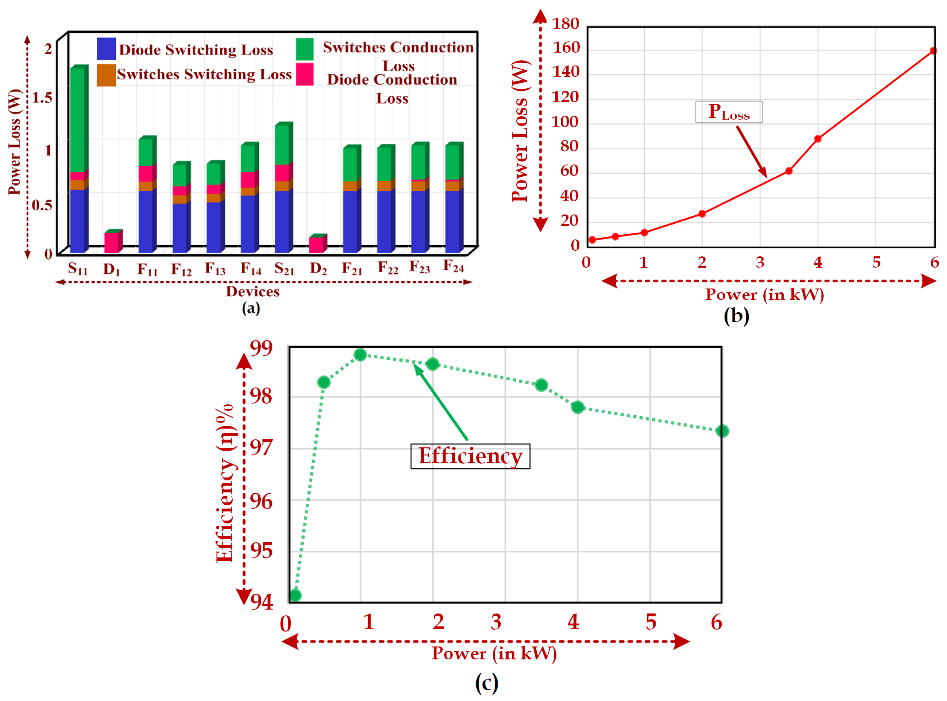
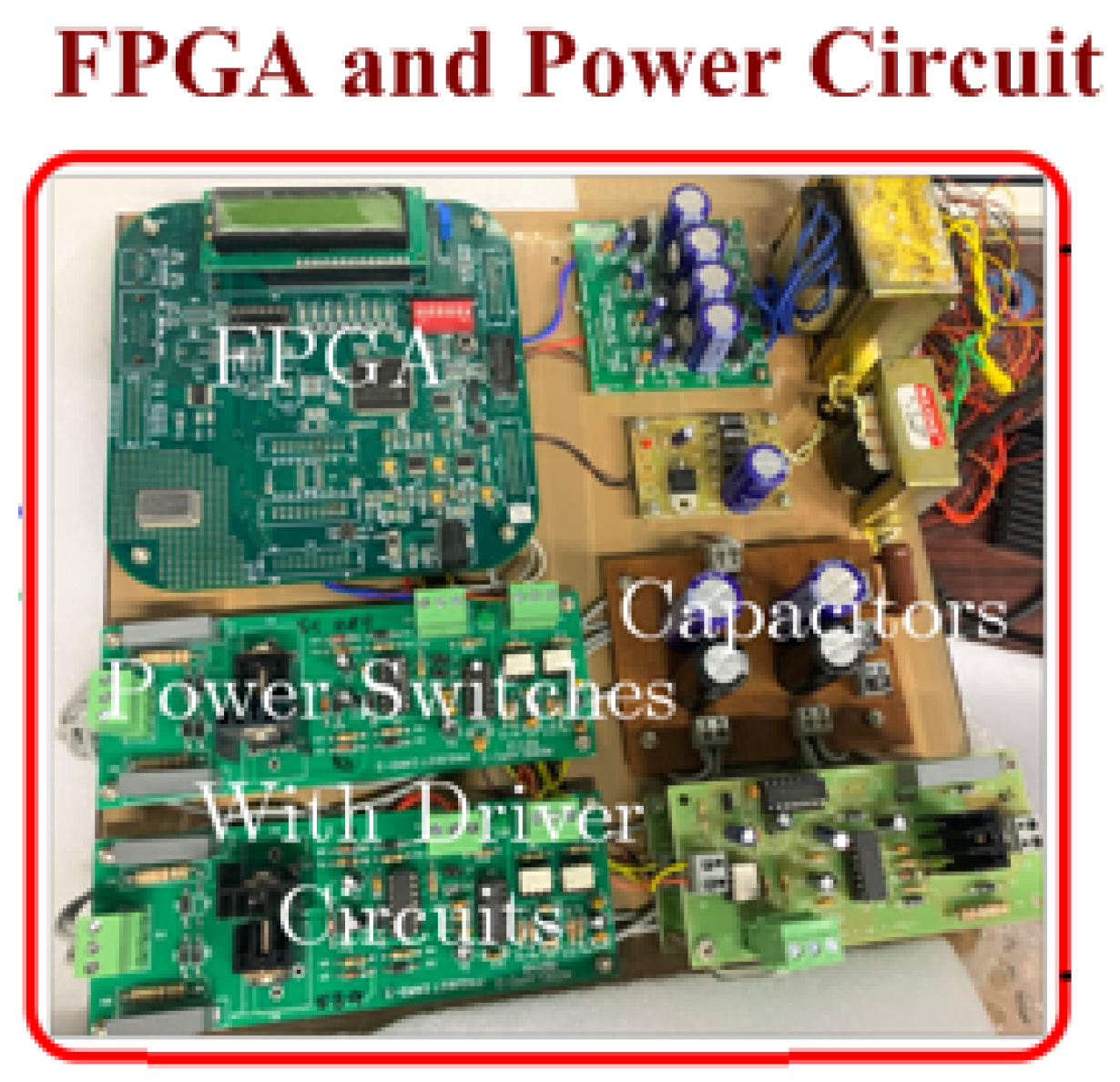
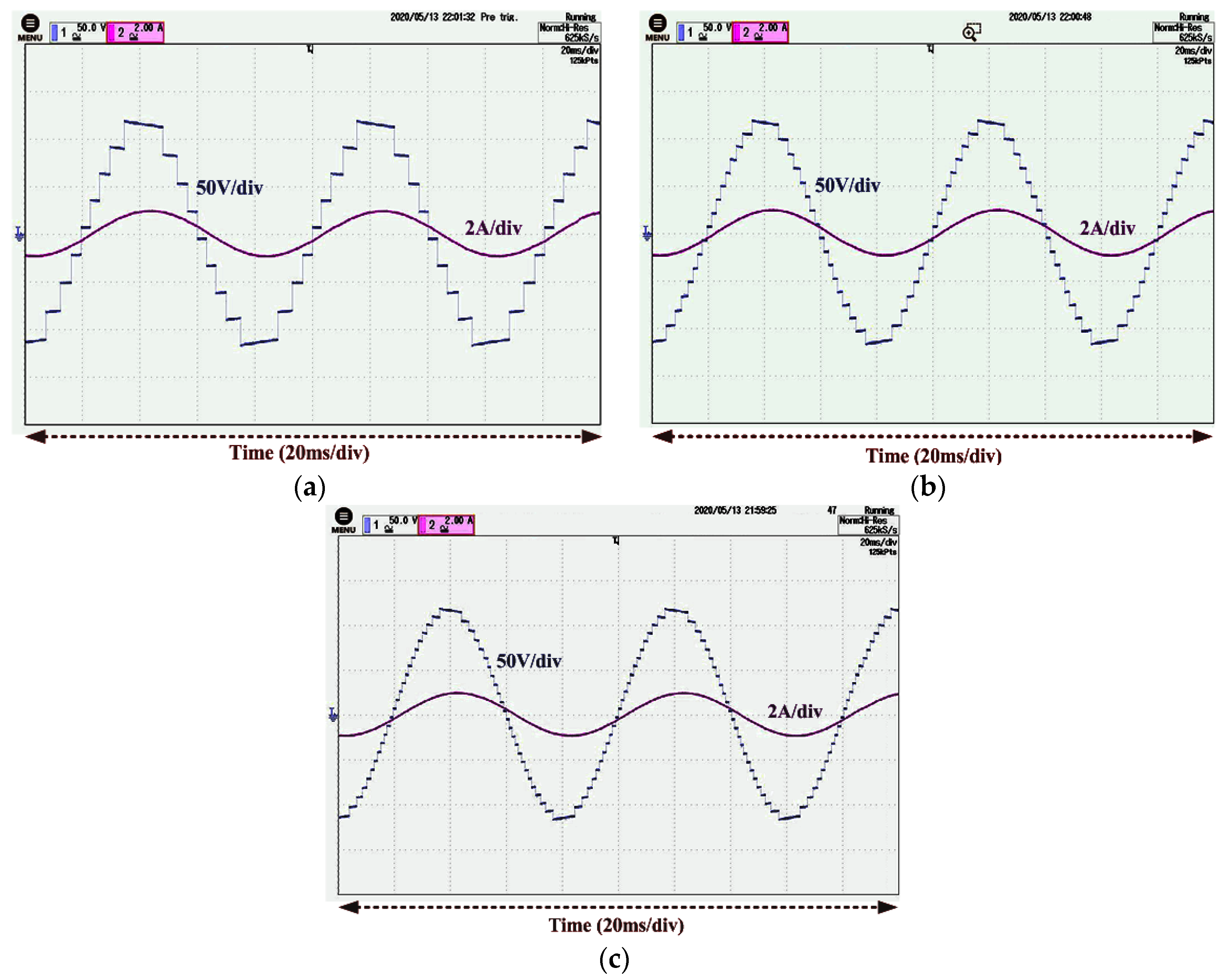
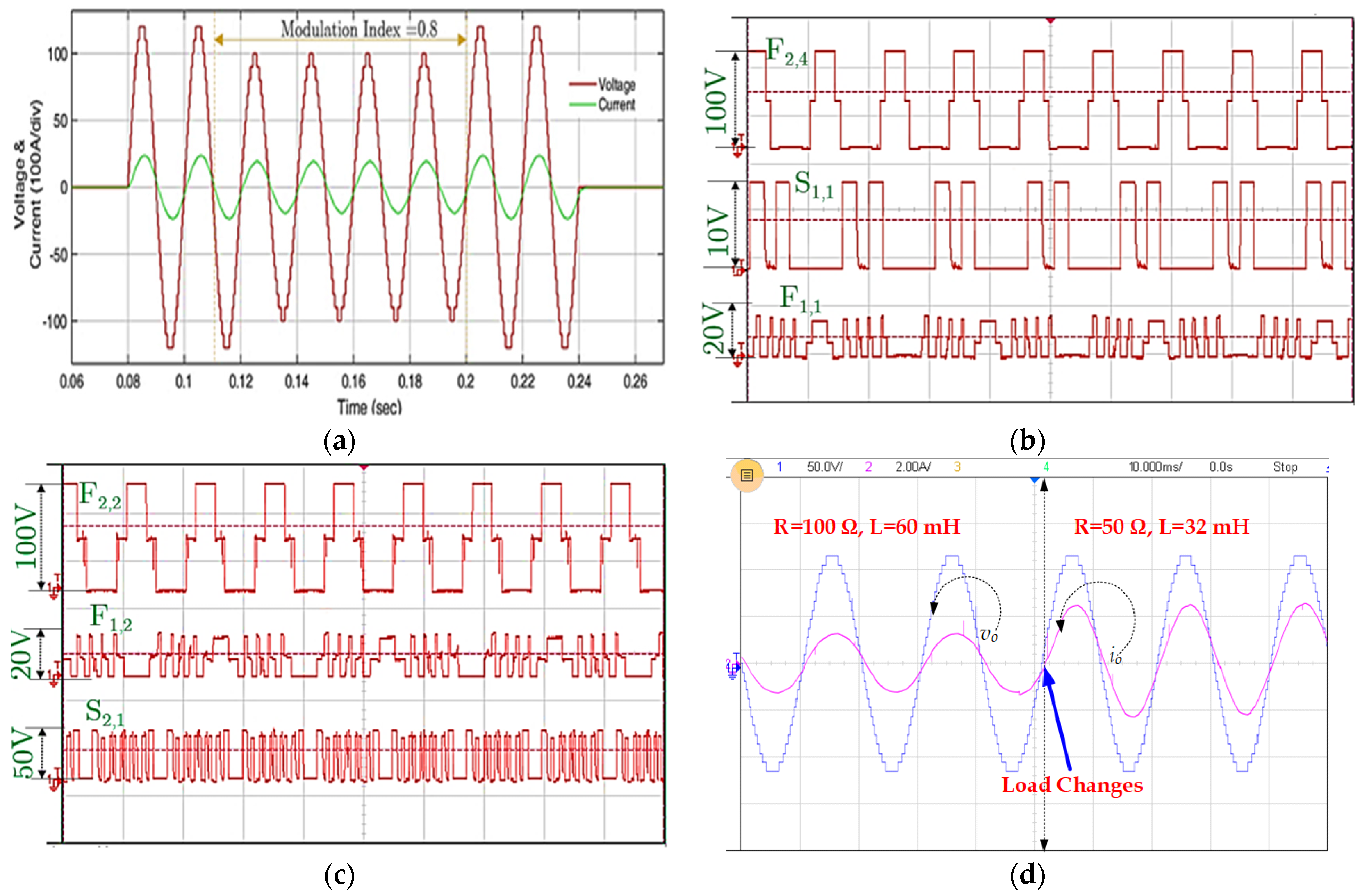
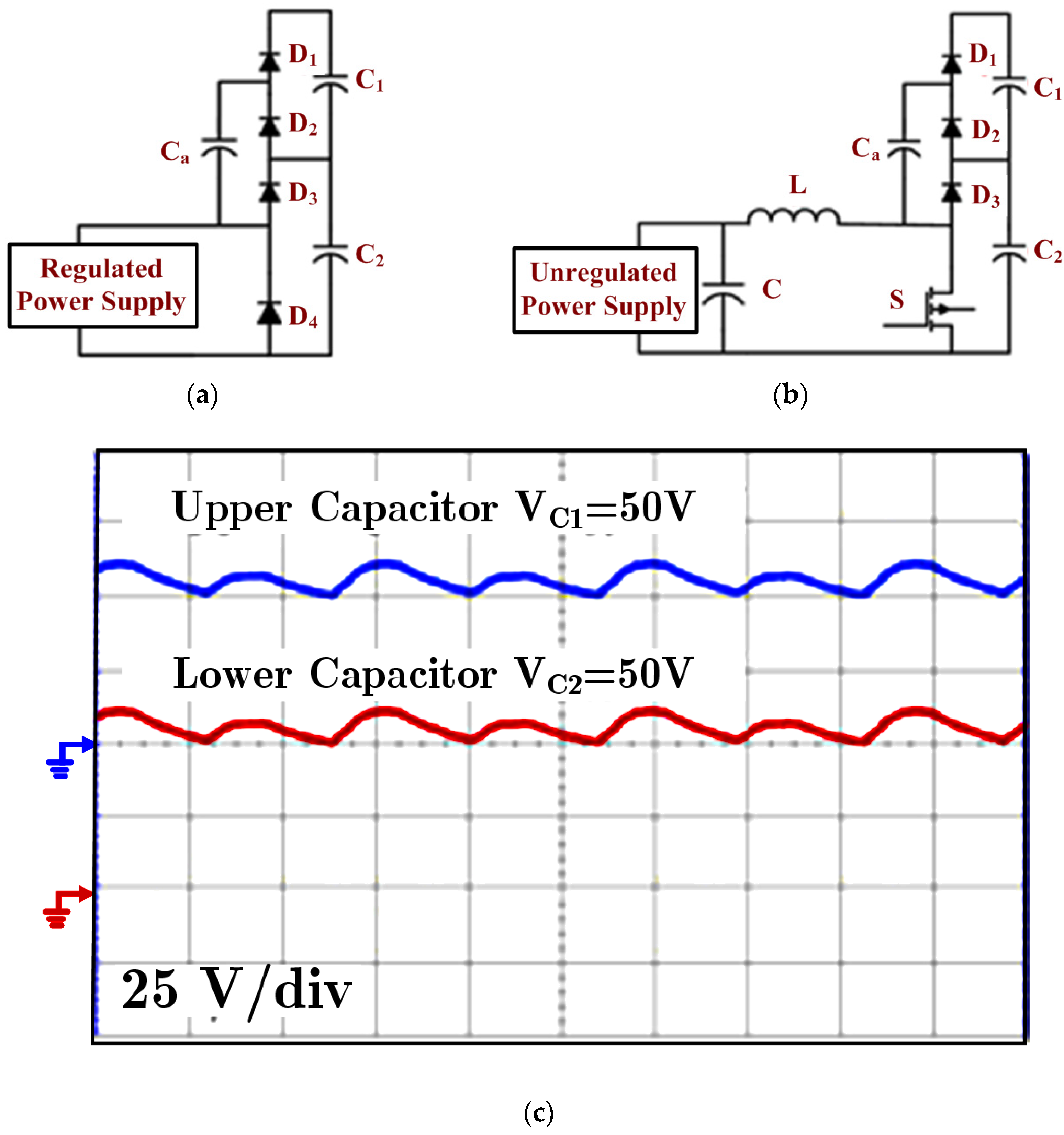
7. Experimental Test Results

The experimental results for a 9-level symmetric topology, 17-level asymmetric topology, and 25-level of the cascaded structure based on the first and the second algorithm at n = 1 and k = 2, respectively, are presented. In the experimental setup, IGBTs (BUP400D), and IGBT drivers (HCPL316j) are used. A resistive-inductive (RL) load with R = 100 Ω and L = 65 mH is used. The prototype of the proposed inverter is shown in Figure 11. The fundamental switching method [18] is implemented via the FPGA 3E Spartan controller. The obtained experimental results for 9-level, 17 level, and 25 levels are shown in Figure 12a–c, respectively.

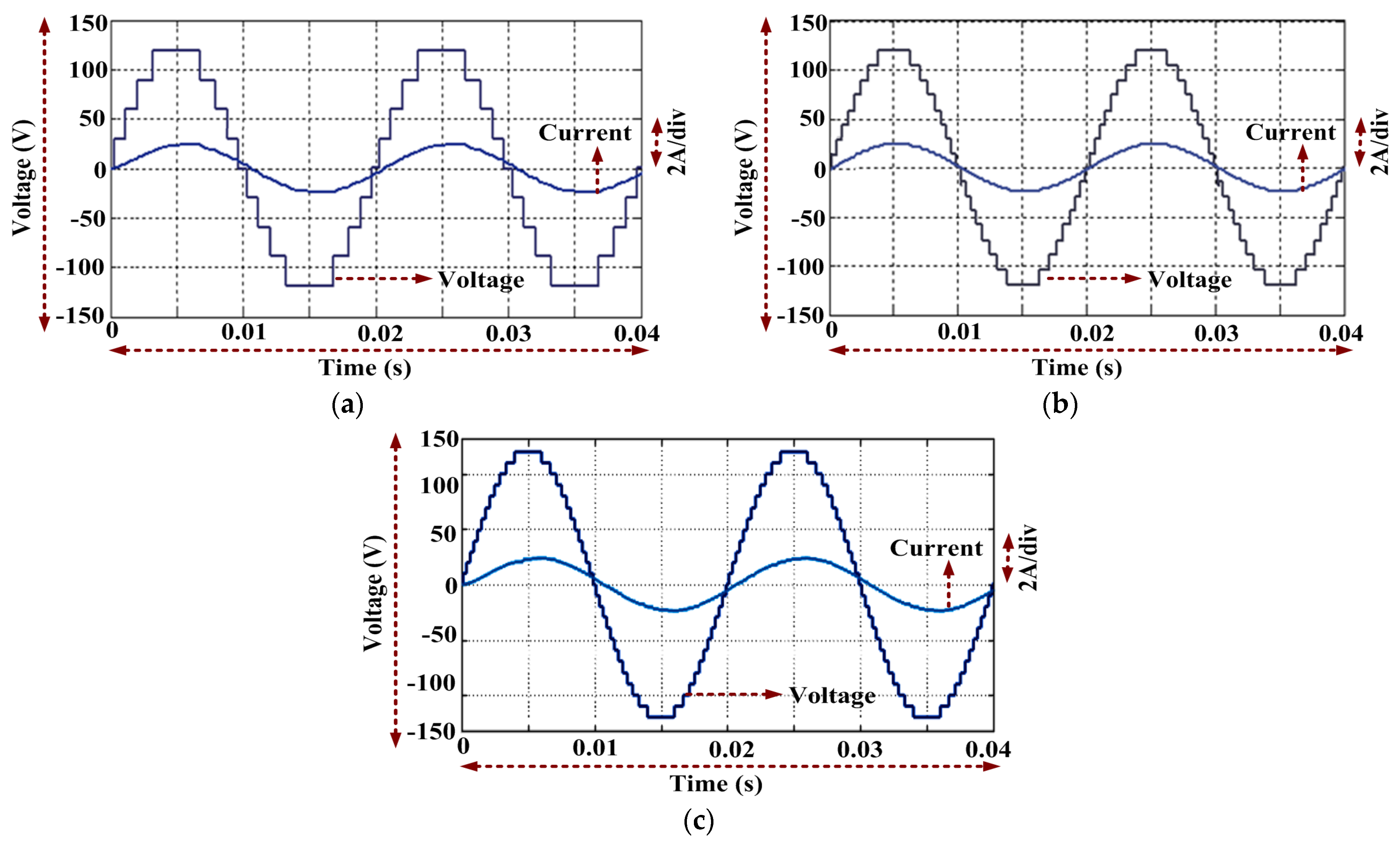
7.1. Symmetric Topology for 9-Level Inverter

Two modules (n = 2) are used with dc source values of 60 volts (V1 = V2 = 60 V) and the voltage across each capacitor equals 30 V to generate the 9-level output voltage waveform in the symmetric configuration. The c output voltage and current waveform with modulation index (Ma = 1) are shown in Figure 12a. To balance the voltage across the capacitors, a voltage balancing circuit that was presented in [23,26] was used. The output frequency is 50Hz with a peak magnitude of 120 V. The maximum blocking voltage across the full-bridge inverter switches is 120 V. The output voltage levels are 0, ±30 V, ±60, ±90 V, and ±120 V. The blocking voltages of the switches are S12 = S22 = 30 V, S11 = S21 = 60 V, and F11 = F12 = F13 = F14 = 120 V for the full-bridge switches. The voltage and current total harmonic distortion (THD) are measured as 9.07% and 2.79%, respectively. Due to the presence of the unidirectional device (diode) the circuit will operate in two- quadrants. Further, the maximum allowable power factor is 0.97 to unity power factor and it is not suitable for high inductive load applications.

7.2. Asymmetric Topology for 17-Level Inverter

For the proposed asymmetric structure, the dc voltage source magnitudes are given as V11 = V12 = 15 V, and V21 = V22 = 45 V for the 17-level with a maximum output voltage (Vo,max) of 120 V. The experimental output voltage waveform is shown in Figure 12b. Two modules (n = 2) are used with eight switches. The maximum blocking voltage of the switches in the module is 30 V and 60 V, respectively, and is 120 V for the full bridge. The output voltage levels are 0, ±15 V, ±30 V, ±45 V … ±120 V, respectively. The voltage and current THD values are measured as 4.76% and 1.45%, respectively.

7.3. Cascaded Asymmetric Structure for 25-Level Inverter

In the cascaded structure, the first and second algorithms result in the same output voltage when n = 1 for the kth unit. In the experimental structure of this work, the MLI is designed for n = 1 and k = 2. The magnitudes of the dc sources are V11 = V12 = 10 V for the first unit and V21 = V22 = 50 V for the second unit. Vo,max equals 20 V and 100 V for the first and second units, respectively. The output voltage and current waveforms for the 25-level are shown in Figure 12c with voltage and current THD values measured as 3.10% and 1.24%, respectively. A comparison of the proposed topologies is given in Table 5. As shown, the cascaded DHB topology requires low blocking voltage and generates a higher number of output voltage levels. In Table 6, the various parameters of the proposed topology with different configurations are compared. Moreover, the dynamic performance of the proposed topology was tested in both simulation and experimental setup.
As shown in Figure 13a for the proposed 25-level topology, it was verified by varying the modulation index. This confirmed that the proposed topology can adjust the load voltage based on the load demand. The experimentally observed voltages across the switches are shown in Figure 13b,c. From the cascaded structure, the first and second unit of switches S1,1, S2,1, F1,1, F1,2, F2,2 and F2,4 shown in Figure 13b,c. As shown, it was validated that the maximum blocking voltage across the switch is 100 V. The experimental performance of the proposed 25-level was tested in the hardware setup by varying the load as shown in Figure 13d. The maximum output voltage was 120 V with a load varying from 0.9 A to 2.2 A (Z = 100 Ω + j 60 Ω to Z = 50 Ω + j 30 Ω). However, the proposed topology is more suitable to operate near the unity power factor due to each module can carry only a positive current due to the presence of the diode. Once again it was proved that the proposed converters are more suitable for distributed- power generation. It should be mentioned that the series-connected dc-link capacitor voltages are balanced using the voltage-divider circuits presented in Figure 14 and this external circuit ensures the balanced capacitor voltages for both high and low switched cells. The circuit in Figure 14a is used for regulated dc sources whilst that in Figure 14b can be used for the unregulated dc sources (like photovoltaic as a source). The experimental balanced output voltage for the second full-bridge inverter is shown in Figure 14c. However, by adding a new dc/dc converter, an extra power conversion stage will be added, but it is here worth mentioning that the overall efficiency will be slightly less than the inverter efficiency. The additional converter is a non-isolated type which introduces the EMI effect during the high duty cycle. The efficiency (η) of the proposed topologies in terms of the number of SMLIs (NSub), blocking voltage, and switches is listed in Table 5.
In Table 6, for the 85-level, two possible combinations are presented: (i) n = 2 with k = 1, and n = 1 with k = 2, which requires a maximum blocking voltage of 34 V in the second SMLI, and (ii) n = 1 with k = 1 and n = 2 with k = 2 with maximum blocking voltage of 40 V is required. Additionally, the various power loss across each device and efficiency (η) are presented in Figure 15a–c, respectively. The major loss depends on the switching scheme of the converter. The fundamental switching methods were used because of their low switching losses. As is obvious, the percentage of losses is low when the output power is high.

8. Conclusions

A new cascaded diode half-bridge multilevel inverter topology is presented in symmetric, asymmetric, and cascaded structures. The symmetric topology is verified at 9-level output voltage and the results confirm the feasibility of the proposed topology. Similarly, asymmetric and cascaded topologies are verified for 17 L and 25 L. However, these topologies limit the high blocking voltage on the full bridge switches. Accordingly, a cascaded structure is proposed to reduce the blocking voltage and generate a higher number of output voltage levels. The cascaded topology is optimized for various parameters, and the results are compared with existing topologies. The prototype model was developed and tested for 130 W. The simulation and experimental results, as well as the comparative study, validate the robustness and effectiveness of the proposed cascaded topology in terms of the reduced power loss, cost, and the number of power electronic components. The maximum simulation efficiency of 98.6% is archived at ~130 W. Finally, the proposed converter is more suitable for distributed-power generation.

Author Contributions

Conceptualization, J.S. and D.A.; methodology, J.S. and R.S.A.; software, J.S.; validation, D.A. and S.H.E.A.A.; formal analysis, J.S. and R.S.A. investigation, K.B.; resources, M.S.B., G.F.S. and K.D.; data curation, D.A.; writing–original draft preparation, J.S.; writing–review and editing, S.H.E.A.A.; supervision, D.A. and K.B.; project administration, J.S. All authors have read and agreed to the published version of the manuscript.

Funding

This research received no external funding.

Institutional Review Board Statement

Not applicable.

Informed Consent Statement

Not applicable.

Data Availability Statement

All data generated or analyzed during this study are included in this article.

Acknowledgments

The authors would like to thank Prince Sultan University, 11586 Riyadh, Saudi Arabia for their support.

Conflicts of Interest

The authors declare no conflict of interest.

References

  1. Sathik, M.A.J.; Vijayakumar, K. An assessment of recent multilevel inverter topologies with reduced power electronics components for renewable applications. Rene. Sustain. Energy Rev. 2018, 82, 3379–3399. [Google Scholar]
  2. Ali, J.S.M.; Krishnasamy, V. Compact Switched-Capacitor Multilevel Inverter (CSCMLI) with Self-Voltage Balancing and Boosting Ability. IEEE Trans. Power Electron. 2019, 34, 4009–4013. [Google Scholar]
  3. Ali, J.S.M.; Alishah, R.S.; Krishnasamy, V. A New Generalized Multilevel Converter Topology with Reduced Voltage on Switches, Power losses, and Components. IEEE J. Emerg. Sel. Top. Power Electron. 2019, 7, 1094–1106. [Google Scholar]
  4. Sathik, J.; Aleem, S.H.E.A.; Kannan, R.; Zobaa, A. A new switched DC-link capacitor-based multi-level converter (SDC 2 MLC). Electr. Power Compon. Syst. 2017, 45, 1001–1015. [Google Scholar] [CrossRef] [Green Version]
  5. Shukla, A.; Ghosh, A.; Joshi, A. Hysteresis Current Control Operation of Flying Capacitor Multilevel Inverter and Its Application in Shunt Compensation of Distribution Systems. IEEE Trans. Power Deliv. 2007, 22, 396–405. [Google Scholar] [CrossRef] [Green Version]
  6. Memon, M.A.; Siddique, M.D.; Saad, M.; Mubin, M. Asynchronous Particle Swarm Optimization-Genetic Algorithm (APSO-GA) based Selective Harmonic Elimination in a Cascaded H-Bridge Multilevel Inverter. IEEE Trans. Ind. Electron. 2021. [Google Scholar] [CrossRef]
  7. Wu, S.; Qi, L.; Jia, W.; Zhu, Y.; Zhang, X.; Guo, X.; Pan, X. A Modular Multilevel Converter with Integrated Energy Dissipation Equipment for Offshore Wind VSC-HVDC System. IEEE Trans. Sustain. Energy 2021. [Google Scholar] [CrossRef]
  8. Newton, C.; Sumner, M. Multilevel converters: A real solution to medium high voltage drives? Inst. Electron. Eng. Power Eng. J. 1998, 12, 21–26. [Google Scholar] [CrossRef]
  9. Lai, J.-S.; Peng, F.Z. Multilevel converters—A new breed of power converters. IEEE Trans. Ind. Appl. 1996, 32, 509–517. [Google Scholar]
  10. Patil, K.V.; Mathur, R.M.; Jiang, J.; Hosseini, S.H. Distribution system compensation using a new binary multilevel voltage source inverter. IEEE Trans. Power Deliv. 1999, 14, 459–464. [Google Scholar] [CrossRef]
  11. Ali, J.S.M.; Alishah, R.S.; Sandeep, N.; Hosseini, S.H.; Babaei, E.; Vijayakumar, K.; Yaragatti, U.R. A New Generalized Multilevel Converter Topology Based on Cascaded Connection of Basic Units. IEEE J. Emerg. Sel. Top. Power Electron. 2019, 7, 2498–2512. [Google Scholar]
  12. Liu, Y.; Luo, F.L. Trinary hybrid 81-level multilevel inverter for motor drive with zero common-mode voltage. IEEE Trans. Ind. Electron. 2008, 55, 1014–1021. [Google Scholar] [CrossRef]
  13. Mokhberdoran, A.; Ajami, A. Symmetric and asymmetric design and implementation of new cascaded multilevel inverter topology. IEEE Trans. Power Electron. 2014, 29, 6712–6724. [Google Scholar] [CrossRef]
  14. Kangarlu, M.F.; Babaei, E.; Laali, S. Symmetric multilevel inverter with reduced components based on non-insulated DC voltage sources. IET Power Electron. 2012, 5, 571–581. [Google Scholar] [CrossRef]
  15. Oskuee, M.R.J.; Karimi, M.; Ravadanegh, S.N.; Gharehpetian, G.B. An Innovative Scheme of Symmetric Multilevel Voltage Source Inverter with Lower Number of Circuit Devices. IEEE Trans. Ind. Electron. 2015, 62, 6965–6973. [Google Scholar] [CrossRef]
  16. Oskuee, M.R.J.; Salary, E.; Najafi-Ravadanegh, S. Creative design of symmetric multilevel converter to enhance the circuit’s performance. IET Power Electron. 2015, 8, 96–102. [Google Scholar] [CrossRef]
  17. Samadaei, E.; Gholamian, S.A.; Sheikholeslami, A.; Adabi, J. An envelope type (E-Type) module: Asymmetric multilevel inverters with reduced components. IEEE Trans. Ind. Electron. 2016, 63, 7148–7156. [Google Scholar] [CrossRef]
  18. Alishah, R.S.; Hosseini, S.H.; Babaei, E.; Sabahi, M. Optimal design of new cascaded switch-ladder multilevel inverter structure. IEEE Trans. Ind. Electron. 2017, 64, 2072–2080. [Google Scholar] [CrossRef]
  19. Alishah, R.S.; Hosseini, S.H.; Babaei, E.; Sabahi, M. A new general multilevel converter topology based on cascaded connection of submultilevel units with reduced switching components, DC sources, and blocked voltage by switches. IEEE Trans. Ind. Electron. 2016, 63, 7157–7164. [Google Scholar] [CrossRef]
  20. Alishah, R.S.; Nazarpour, D.; Hosseini, S.H.; Sabahi, M. Reduction of power electronic elements in multilevel converters using a new cascade structure. IEEE Trans. Ind. Electron. 2015, 62, 256–269. [Google Scholar] [CrossRef]
  21. Ebrahimi, J.; Babaei, E.; Gharehpetian, G.B. A new topology of cascaded multilevel converters with reduced number of components for high-voltage applications. IEEE Trans. Power Electron. 2011, 26, 3109–3118. [Google Scholar] [CrossRef]
  22. Ebrahimi, J.; Babaei, E.; Gharehpetian, G.B. A new multilevel converter topology with reduced number of power electronic components. IEEE Trans. Ind. Electron. 2012, 59, 655–667. [Google Scholar] [CrossRef]
  23. Samanbakhsh, R.; Taheri, A. Reduction of power electronic components in multilevel converters using new switched capacitor-diode structure. IEEE Trans. Ind. Electron. 2016, 63, 7204–7214. [Google Scholar] [CrossRef]
  24. Prabaharan, N.; Salam, Z.; Cecati, C.; Palanisamy, K. Design and implementation of new multilevel inverter topology for trinary sequence using unipolar pulse width modulation. IEEE Trans. Ind. Electron. 2020, 67, 3573–3582. [Google Scholar] [CrossRef]
  25. Rosas-Caro, J.C.; Ramirez, J.M.; Peng, F.Z.; Valderrabano, A. A DC–DC multilevel boost converter. IET Power Electron. 2010, 3, 129–137. [Google Scholar] [CrossRef]
  26. Taheri, A.; Rasulkhani, A.; Ren, H.-P. An Asymmetric Switched Capacitor Multilevel Inverter with Component Reduction. IEEE Access 2019, 7, 127166–127176. [Google Scholar] [CrossRef]
  27. Zaid, M.M.; Ro, J.-S. Switch Ladder Modified H-Bridge Multilevel Inverter with Novel Pulse Width Modulation Technique. IEEE Access 2019, 7, 102073–102086. [Google Scholar] [CrossRef]
  28. Siddique, M.D.; Mekhilef, S.; Shah, N.M.; Sarwar, A.; Iqbal, A.; Tayyab, M.; Ansari, M.K. Low Switching Frequency Based Asymmetrical Multilevel Inverter Topology with Reduced Switch Count. IEEE Access 2019, 7, 86374–86383. [Google Scholar] [CrossRef]
  29. Dhanamjayulu, C.; Meikandasivam, S. Implementation and Comparison of Symmetric and Asymmetric Multilevel Inverters for Dynamic Loads. IEEE Access 2018, 6, 738–746. [Google Scholar] [CrossRef]
  30. Almakhles, D.J.; Ali, J.S.M.; Padmanaban, S.; Bhaskar, M.S.; Subramaniam, U.; Sakthivel, R. An Original Hybrid Multilevel DC-AC Converter Using Single-Double Source Unit for Medium Voltage Applications: Hardware Implementation and Investigation. IEEE Access 2020, 8, 71291–71301. [Google Scholar] [CrossRef]
  31. Meraj, S.T.; Hasan, K.; Masaoud, A. A Novel Configuration of Cross-Switched T-Type (CT-Type) Multilevel Inverter. IEEE Trans. Power Electron. 2019, 35, 3688–3696. [Google Scholar] [CrossRef]
  32. Panda, K.P.; Bana, P.R.; Panda, G. FPA Optimized Selective Harmonic Elimination in Symmetric–Asymmetric Reduced Switch Cascaded Multilevel Inverter. IEEE Trans. Ind. Appl. 2020, 56, 2862–2870. [Google Scholar] [CrossRef]
  33. Ali, S.; Ling, Z.; Tian, K.; Huang, Z. Recent Advancements in Submodule Topologies and Applications of MMC. IEEE J. Emerg. Sel. Top. Power Electron. 2021, 9, 3407–3435. [Google Scholar] [CrossRef]
  34. Deng, F.; Lü, Y.; Liu, C.; Heng, Q.; Yu, Q.; Zhao, J. Overview on submodule topologies, modeling, modulation, control schemes, fault diagnosis, and tolerant control strategies of modular multilevel converters. Chin. J. Electr. Eng. 2020, 6, 1–21. [Google Scholar] [CrossRef]
  35. Wang, K.; Zhou, L.; Deng, Y.; Lu, Y.; Wang, C.; Xu, F. Application range analysis and implementation of the logic-processed CPS-PWM scheme based mmc capacitor voltage balancing strategy. CPSS Trans. Power Electron. Appl. 2019, 4, 1–9. [Google Scholar] [CrossRef]
  36. Joshi, S.D.; Ghat, M.B.; Shukla, A.; Chandorkar, M.C. Improved Balancing and Sensing of Submodule Capacitor Voltages in Modular Multilevel Converter. IEEE Trans. Ind. Appl. 2021, 57, 537–548. [Google Scholar] [CrossRef]
  37. Zhao, J.; Kong, C.; Liu, T.; Li, R. Research on an Auto-Optimized Capacitor Voltage Balancing Control Strategy of MMC SM for Renewable Energy HVDC Transmission System. Electronics 2019, 8, 104. [Google Scholar] [CrossRef] [Green Version]
  38. Lara, J.; Masisi, L.; Hernandez, C.; Arjona, M.A.; Chandra, A. Novel Single-Phase Grid-Tied NPC Five-Level Converter with an Inherent DC-Link Voltage Balancing Strategy for Power Quality Improvement. Energies 2021, 14, 2644. [Google Scholar] [CrossRef]
Figure 1. Basic module of proposed converter.
Energies 14 07249 g001
Figure 2. Proposed SDHB multilevel inverter topology.
Energies 14 07249 g002
Figure 3. Proposed ADHB multilevel inverter topology.
Energies 14 07249 g003
Figure 4. Comparison of NIGBT versus NLevel for the proposed topologies with other recent MLI topologies (a) Symmetric DHB, (b) Asymmetric DHB.
Energies 14 07249 g004
Figure 5. Generalized structure of the proposed cascaded ADHB multilevel inverter topology.
Energies 14 07249 g005
Figure 6. Comparison of proposed topology with various topologies algorithms for (a) NLevel with constant NIGBTs, (b) NIGBTs with constant NLevel, (c) NLevel with constant Nsource, (d) Ncapacitor with constant NLevel.
Energies 14 07249 g006
Figure 7. Comparison of proposed topology with various topologies algorithms for (a) Ndriver with constant NLevel, (b) Ndiode with constant NLevel.
Energies 14 07249 g007
Figure 8. Comparison (a) NIGBTS versus levels (b) Ndriver versus levels, (c) Ncapacitor versus levels (d) Nsource versus levels, (e) TBlock versus levels (f) Cost versus levels.
Energies 14 07249 g008
Figure 9. Simulation output voltage and current waveform results (a) 9-Level, (b) 17-Level, (c) 25-Level.
Energies 14 07249 g009
Figure 10. Nearest Level Modulation Technique (a) Stepped voltage waveform and (b) schematic block diagram.
Energies 14 07249 g010
Figure 11. Experimental setup of proposed converter.
Energies 14 07249 g011
Figure 12. Experimental output voltage and current waveform results (a) 9-Level, (b) 17-Level, (c) 25-Level.
Energies 14 07249 g012
Figure 13. Performance assessment (a) Simulation results for various modulation (b) Experimental blocking voltage of switches F2,1, S1,1 and F1,1 (c) Experimental blocking voltage of switches F2,2, F1,2, and S2,1, (d) Experimental dynamic performance of the proposed 25-Level converter.
Energies 14 07249 g013
Figure 14. Circuit diagram of the voltage divider (a) For regulated dc sources, (b) For unregulated dc sources, (c) Capacitors’ balanced waveforms for the 25-Level: second unit.
Energies 14 07249 g014
Figure 15. Plots (a) Various power loss for each device (b) Power loss versus power, (c) efficiency versus power.
Energies 14 07249 g015
Table 1. Switching Sequence of the Proposed Basic Module.
StateSxD1SyVoltage (Vo,max)
00000
1011Vdc
21012Vdc
Table 2. Switching Sequence of the Proposed Symmetric Topology.
StateON/OFF State SwitchesOutput Voltage
S11S21S31S12S22Sn1F11F13
0000000100
100000011+Vn
200000111+2Vn
n − 1011111112 i = 1 n V n 1
n111111112 i = 1 n V n
Table 3. Switching Sequence of the Proposed Asymmetric Topology.
StateON/OFF State SwitchesOutput Voltage
S11S21S31S12S22Sn1F11F13
0000000100
100010011+Vn
210010011+2Vn
3000 01011+3Vn
n − 1011111112 i = 1 n V n 1
n111111112 i = 1 n V n
Table 4. Comparison of proposed topology and other recent MLI topologies [27,28,29,30].
TopologiesNLevelNSwitchesNDiodeNDriverMBlockTBlockEfficiency (%)Voltage THD (%)
Proposed97374Vdc20Vdc94.50%9.07%
178488 Vdc44Vdc94.76%4.76%
251041010Vdc66Vdc95.10%3.10%
[12]1710-108Vdc36Vdc93.91%6.17%
[27]2510161012Vdc70Vdc99.7%3.25%
[28]178888Vdc36Vdc98.5%6.8%
[29]2514-1112Vdc76VdcNANA
[30]17108108Vdc36Vdc96.7%5.41%
Table 5. Comparison of the proposed symmetric, asymmetric, and cascaded Configuration.
DescriptionSymmetricAsymmetricCascaded
VBlock in volts120120100
Number of switches8810
Number of driver circuit8810
Variety of dc source122
Nsource/Ncapacitors2/42/42/4
Number of levels91725
Voltage THD (%)Experimental9.07%4.76%3.10%
Simulation8.78%4.69%2.97%
Table 6. Comparison of proposed topology for various output voltage levels for same power rating.
NumberNswitchVBlock (V)NLevelTBlock (V)Nsource/NcapacitorNSubη (%)
162 5111/2188.12
2849222/4188.9
38817442/4189.46
4121025662/4289.97
51434852313/6290.11
61440852313/6290.37
718501253413/6390.23
Publisher’s Note: MDPI stays neutral with regard to jurisdictional claims in published maps and institutional affiliations.

