
Effect of the Heat Dissipation System on Hard-Switching GaN-Based Power Converters for Energy Conversion

 ,
,  ,
,  , ,
, ,
Abstract
:
1. Introduction
- A study of the different dissipation strategies and a comparison in terms of thermal efficiency;
- An analysis of the relationship between the TIM and the effectiveness of the dissipation system;
- A detailed discussion on how to model GaN converters, including their dissipation system and the parameters that affect losses and junction temperature;
- A quantification of the impact of the dissipation system on the parasitic inductance of the power converter.
2. Thermal Dissipation
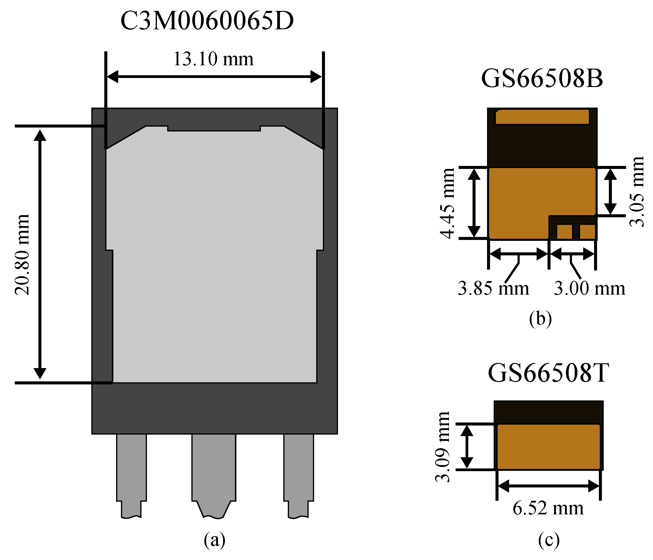
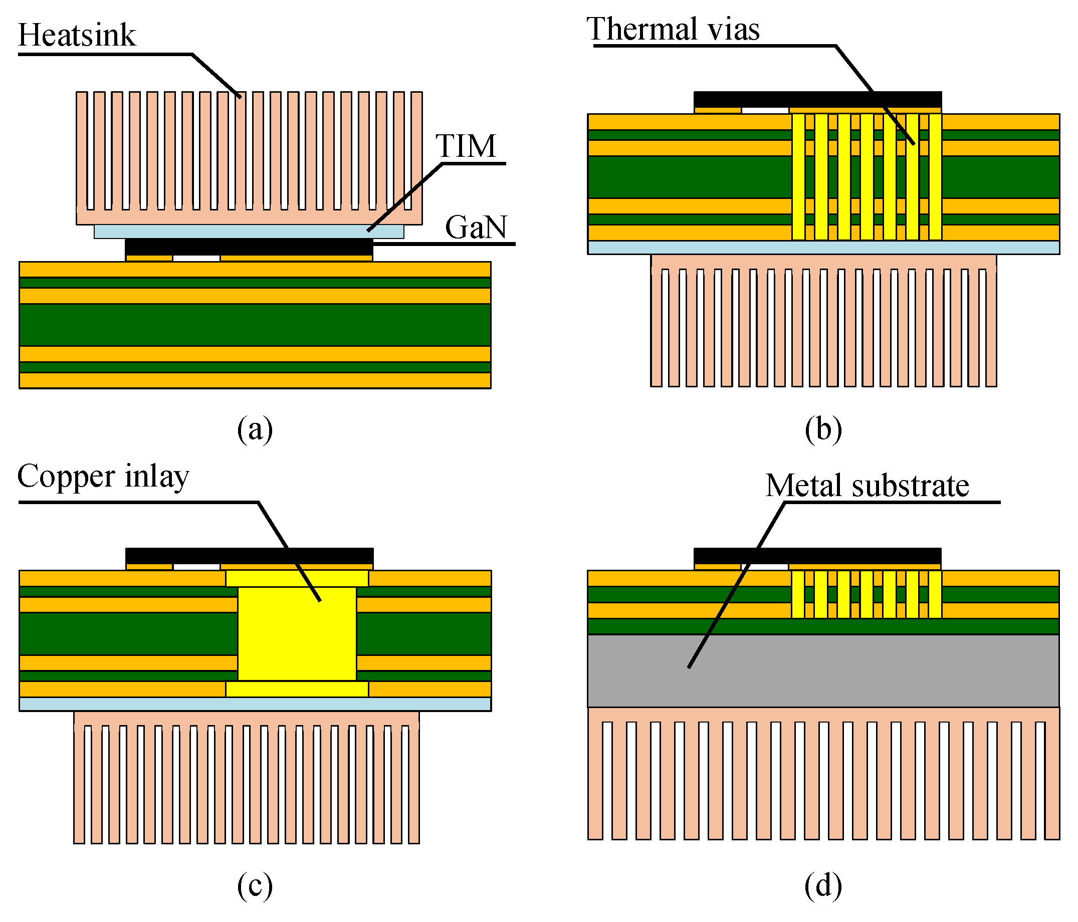
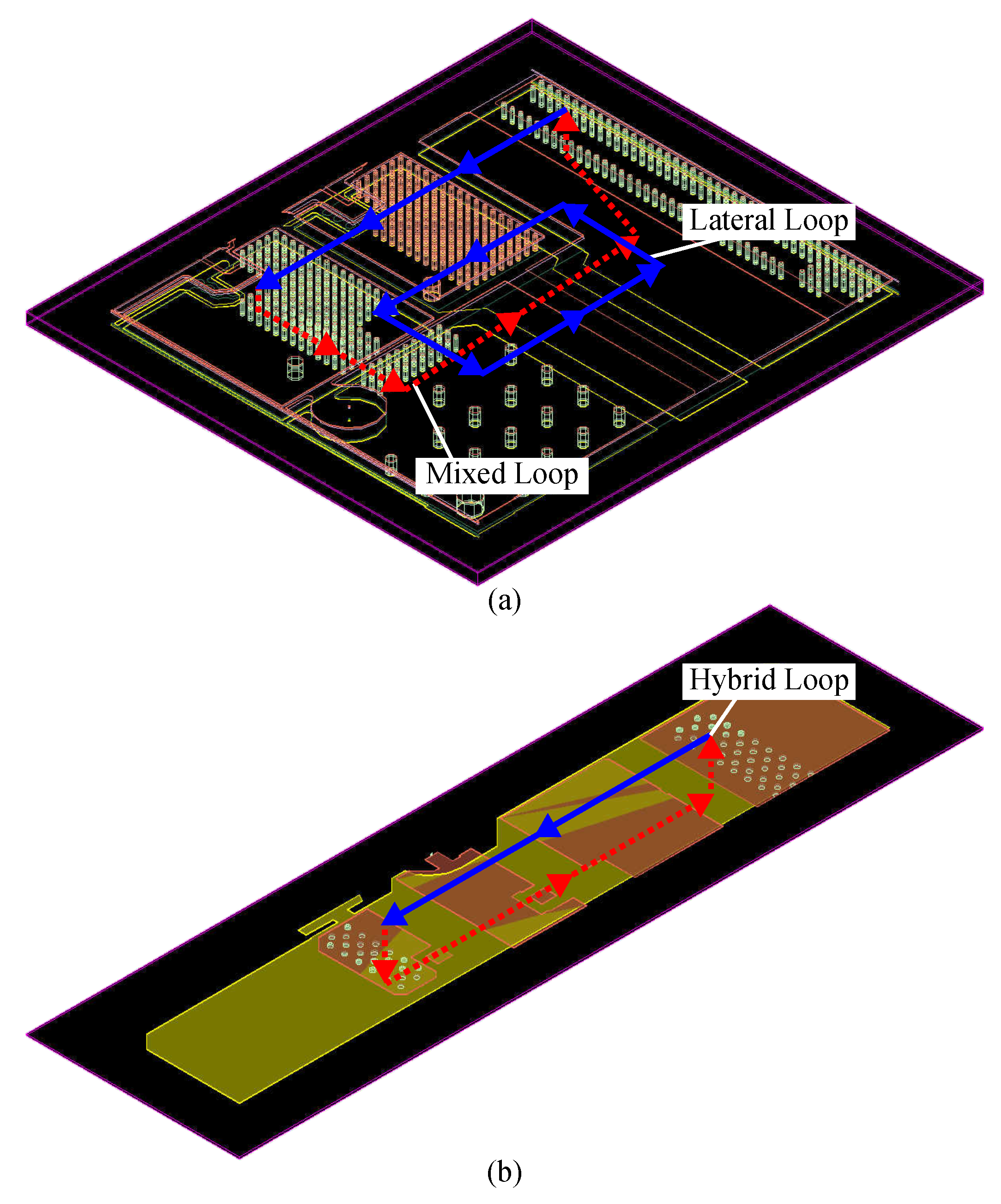
2.1. PCB Structure
2.2. Thermal Interface Materials
- Thermal conductivity: determines the capacity to conduct heat. Materials with a high thermal conductivity easily transfer heat;
- Thermal resistance: measures the difficulty with which heat flows through a component. It should be as low as possible to ensure good dissipation. Thermal resistance is defined aswhere e is the thickness, A is the cross-sectional area perpendicular to the heat flow path, is the thermal conductivity, and and are the contact resistances of the TIM with adjacent surfaces;
- Mounting pressure: directly influences the thermal resistance of the TIM (see Equation (2)). Each material requires a different pressure to minimise contact resistance [57,58]. Inadequate pressure can increase the thermal resistance and cause GaN e-HEMTs to overheat [27]. Importantly, some GaN e-HEMTs only tolerate pressures below 690 kPa (100 psi) [28];
- Dielectric breakdown voltage: is the maximum voltage that a dielectric can withstand without becoming electrically conductive. This voltage depends, amongst others, on the size, shape, and material of the TIM [59].
3. Power Converter Modelling and Simulation Results
- The heatsink does not affect the parasitic capacitance;
- The temperature inside the GaN e-HEMT is homogeneous;
- There is no gate driver loss.
3.1. Thermal Modelling
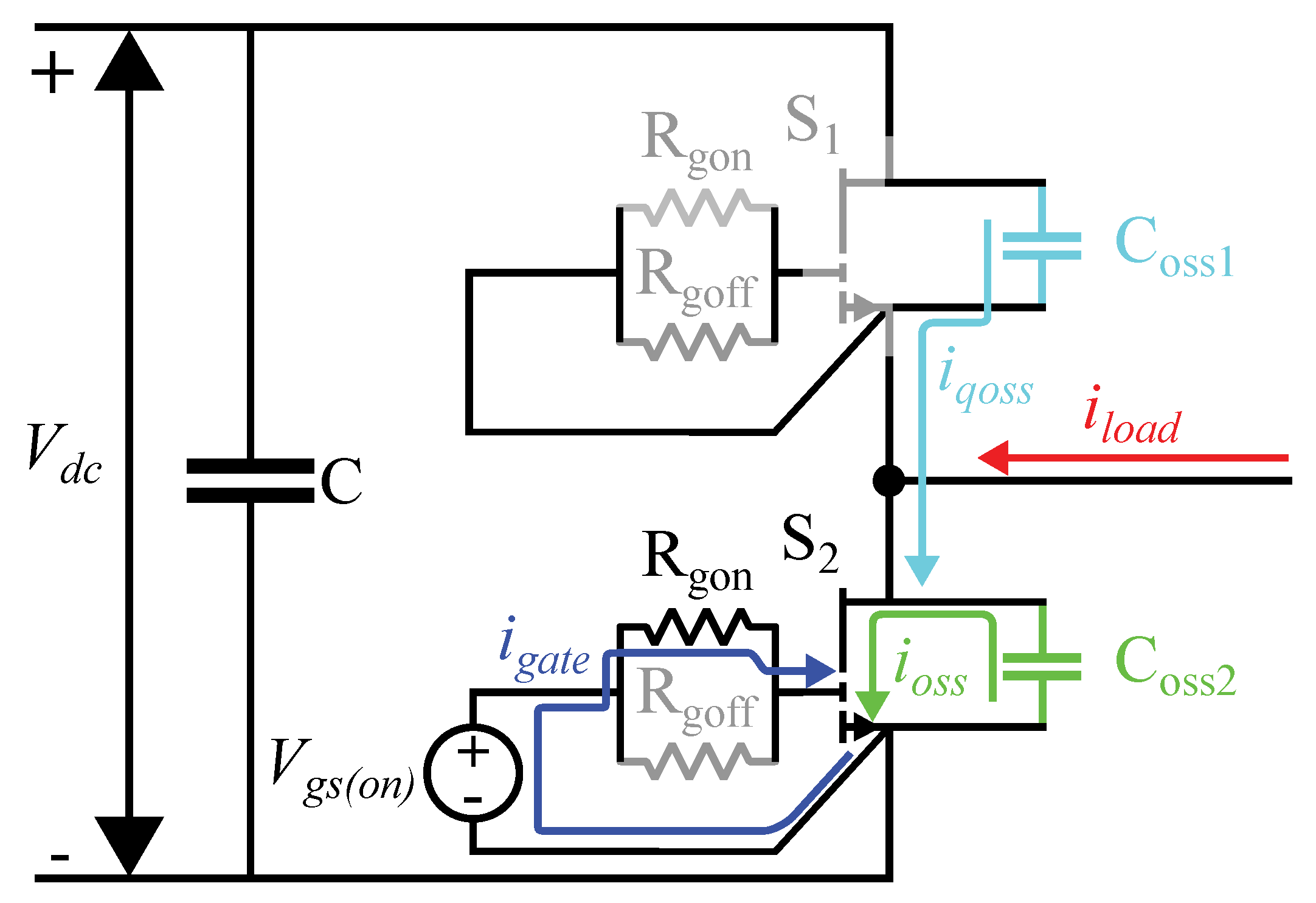
3.2. Electrical Modelling
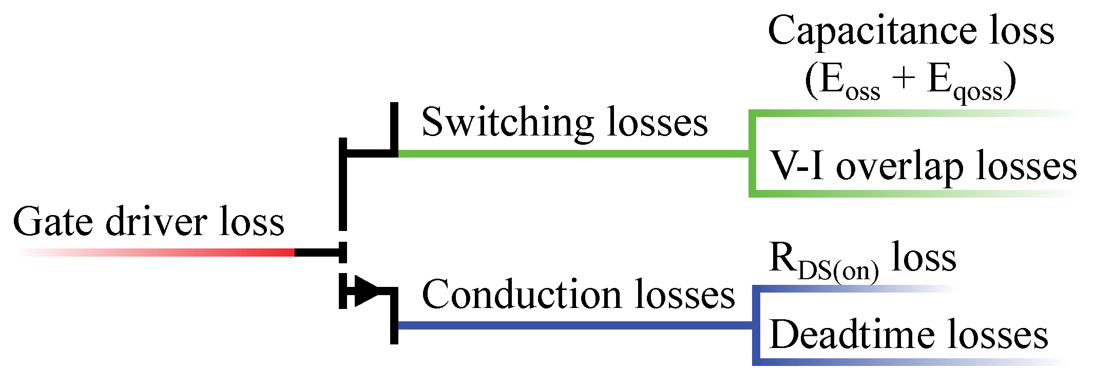
3.2.1. Gate Driver Loss
3.2.2. Switching Losses
3.2.3. Conduction Losses
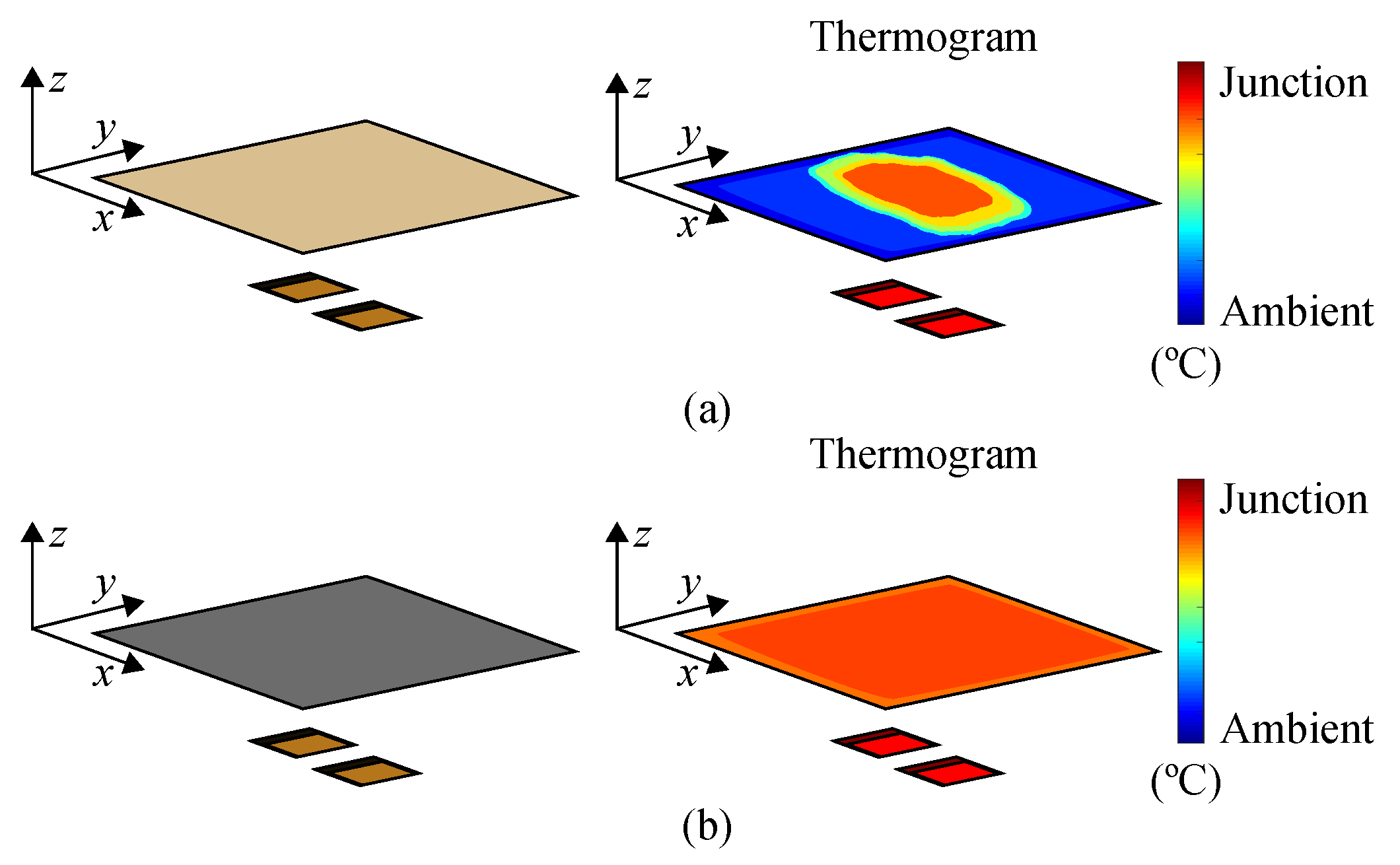
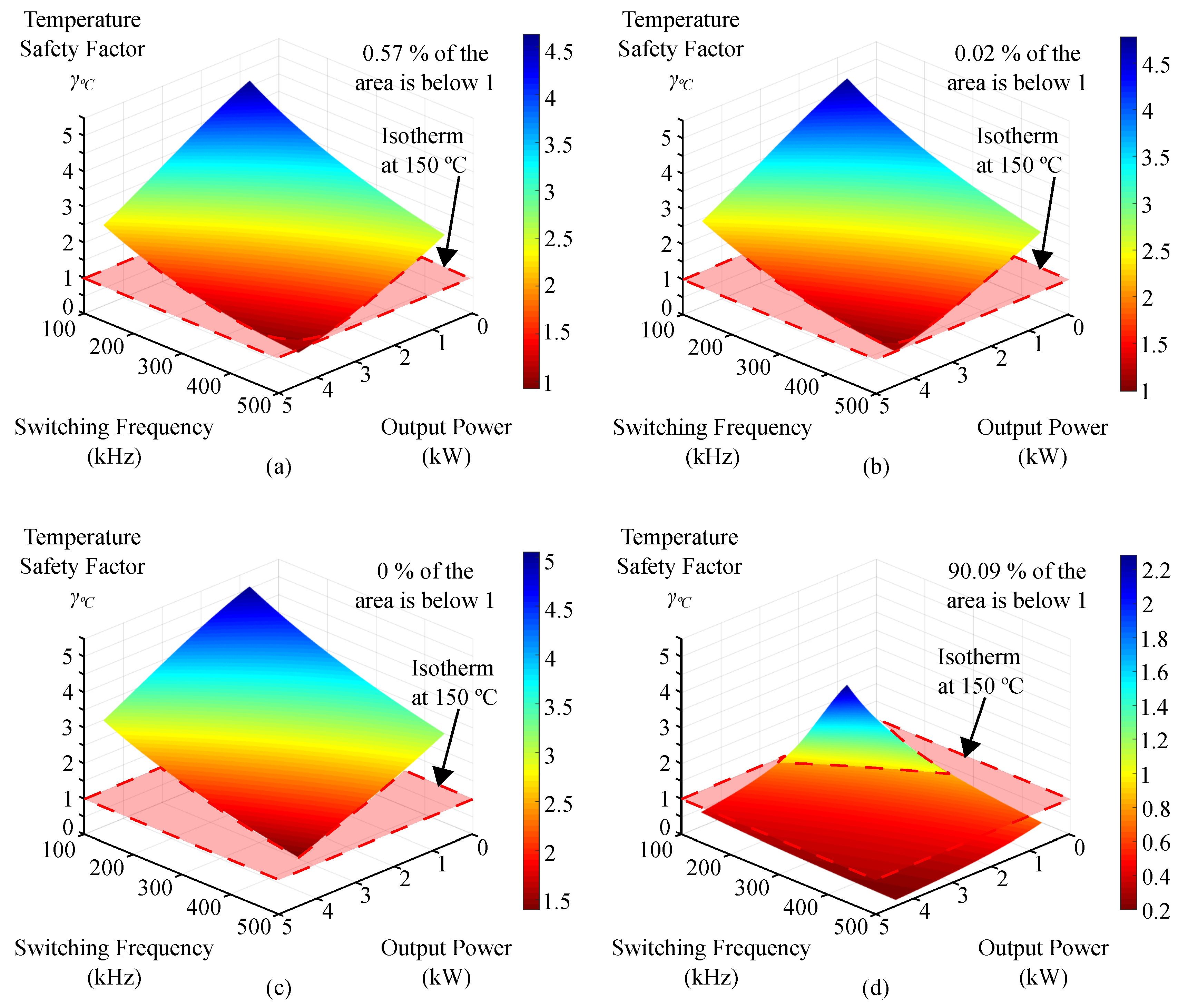
3.3. Temperature Analysis
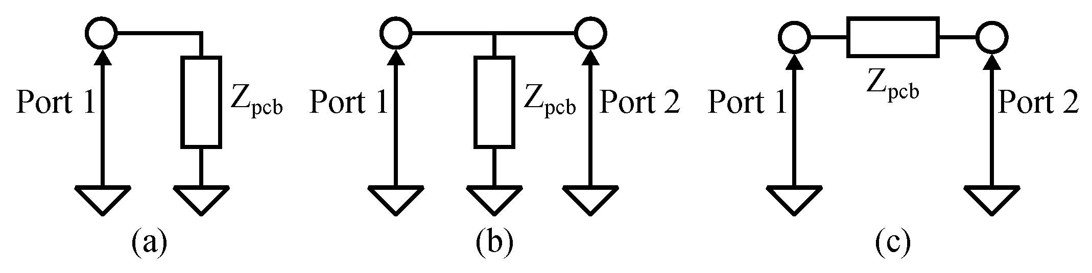
3.4. Parasitic Inductance Modelling
3.5. Parasitic Elements Analysis
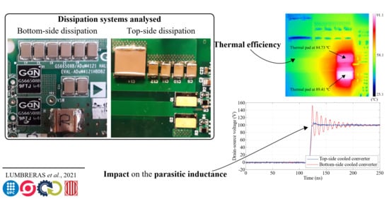
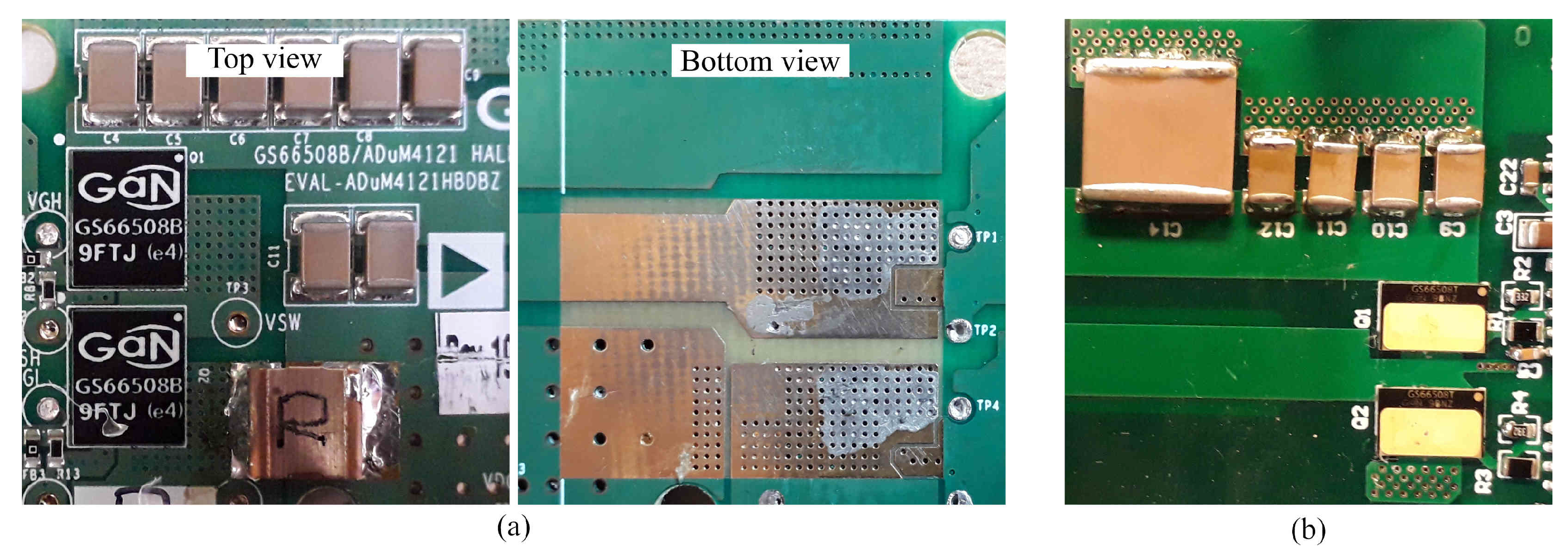
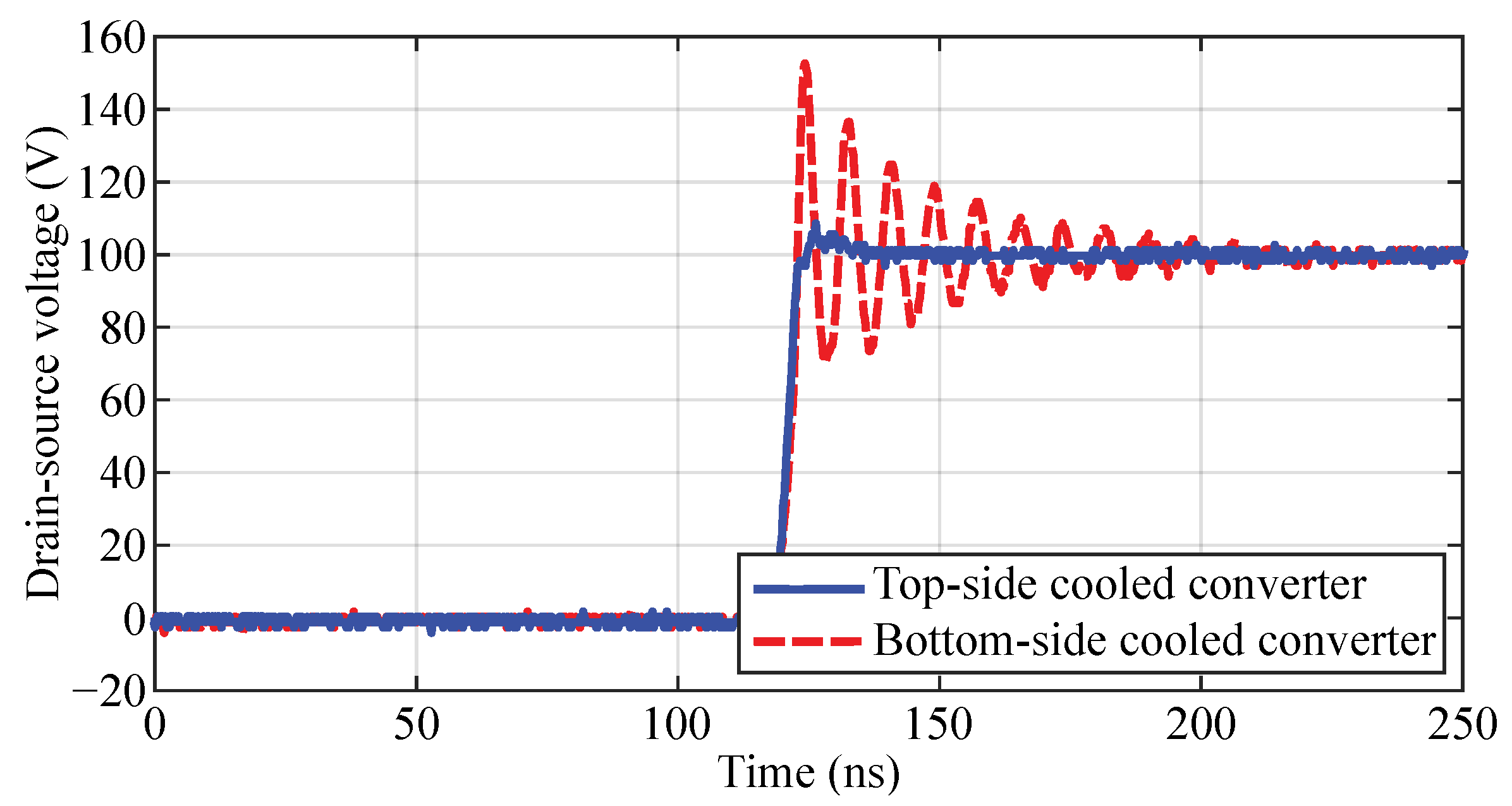
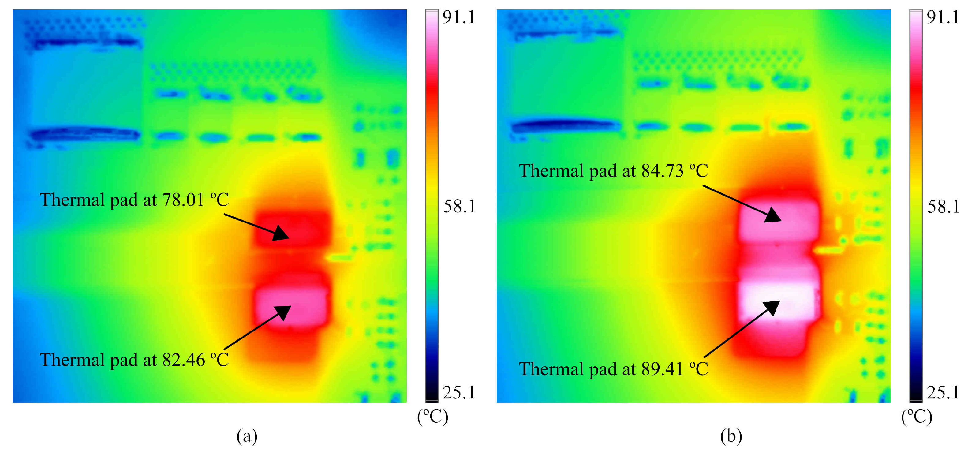
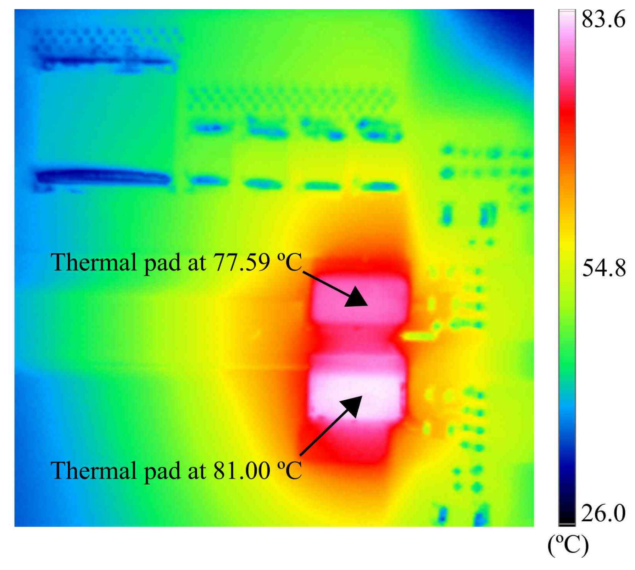
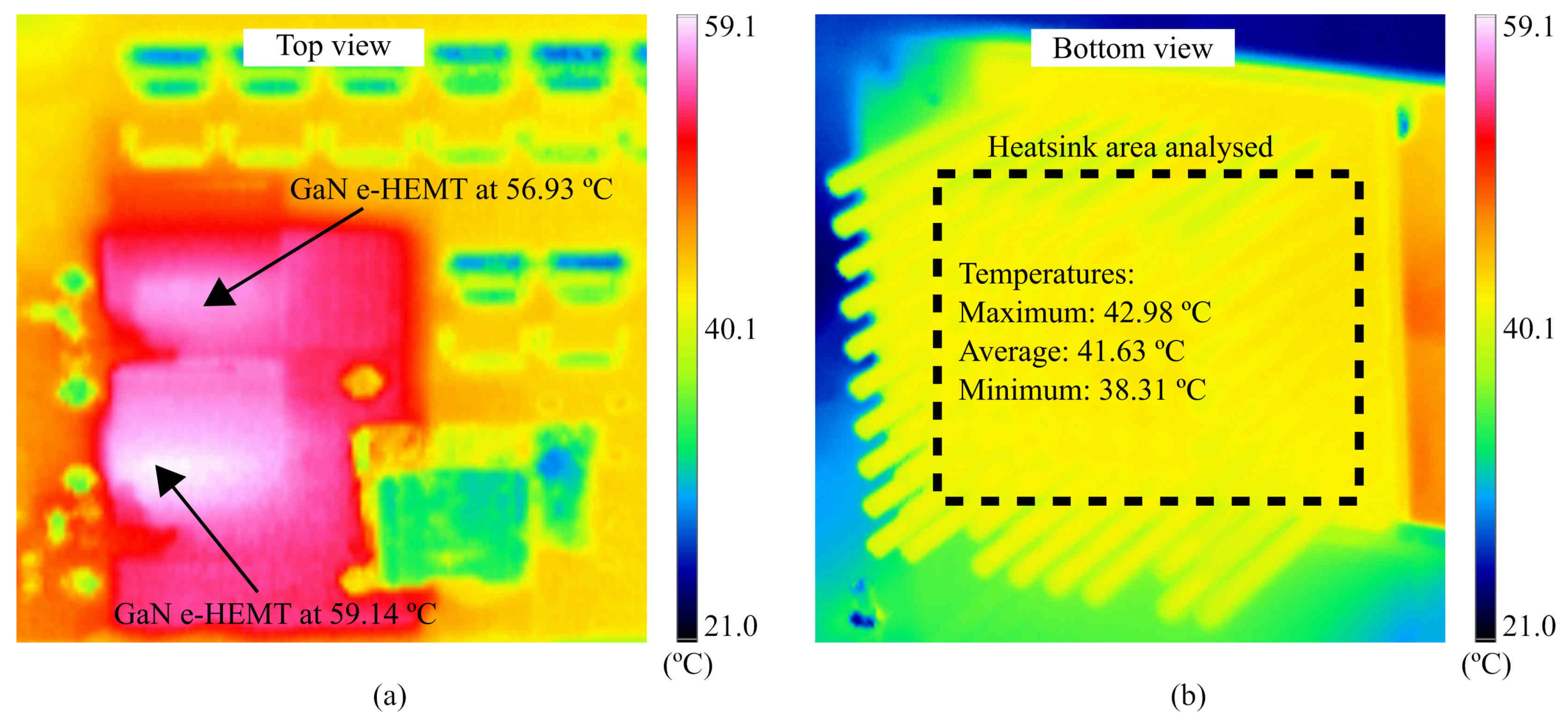
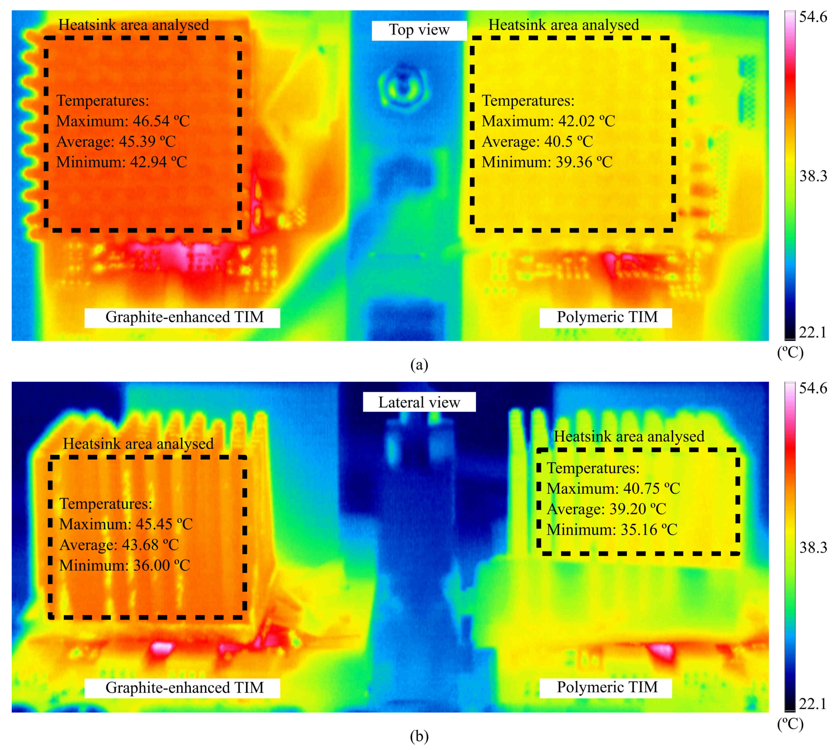
4. Experimental Results
5. Conclusions
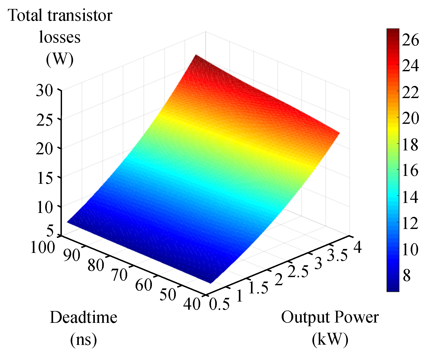
- Deadtime has a significant influence on losses, especially when working with high power;
- Bottom-cooled power converters exhibit significant parasitic inductance and, therefore, high voltage ringing. This behaviour is due to the presence of thermal vias. The vias prevent the current from flowing directly below the transistors, so the power loop has to be closed over a longer path, which increases the parasitic inductance;
- Top-cooled power converters allow for a more optimised layout than bottom-cooled converters since the former do not require thermal vias. Thus, the parasitic inductance may be minimal. However, due to the small size of GaN e-HEMTs, these converters require TIMs with high thermal conductivity to properly extract heat from the transistors.
Author Contributions
Funding
Institutional Review Board Statement
Informed Consent Statement
Data Availability Statement
Conflicts of Interest
Abbreviations
| ADS | Advanced design system |
| EV | Electric vehicle |
| EMI | Electromagnetic interference |
| e-HEMT | Enhancement-mode high-electron-mobility transistors |
| IMS | Insultaded metal substrate |
| GaN | Gallium nitride |
| PLECS | Piecewise linear electrical circuit simulation |
| SiC | Silicon carbide |
| TIM | Thermal interface material |
| WBG | Wide-bandgap |
References
- Millan, J.; Godignon, P.; Perpina, X.; Perez-Tomas, A.; Rebollo, J. A survey of wide bandgap power semiconductor devices. IEEE Trans. Power Electron. 2014, 29, 2155–2163. [Google Scholar] [CrossRef]
- Shenai, K. High-Density Power Conversion and Wide-Bandgap Semiconductor Power Electronics Switching Devices. Proc. IEEE 2019, 107, 2308–2326. [Google Scholar] [CrossRef]
- Shenai, K. Wide bandgap (WBG) semiconductor power converters for DC microgrid applications. In Proceedings of the 2015 IEEE First International Conference on DC Microgrids (ICDCM), Atlanta, GA, USA, 7–10 June 2015; pp. 263–268. [Google Scholar] [CrossRef]
- Xue, F.; Yu, R.; Huang, A.Q. A 98.3% Efficient GaN Isolated Bidirectional DC-DC Converter for DC Microgrid Energy Storage System Applications. IEEE Trans. Ind. Electron. 2017, 64, 9094–9103. [Google Scholar] [CrossRef]
- Mishima, T.; Morita, E. High-Frequency Bridgeless Rectifier Based ZVS Multiresonant Converter for Inductive Power Transfer Featuring High-Voltage GaN-HFET. IEEE Trans. Ind. Electron. 2017, 64, 9155–9164. [Google Scholar] [CrossRef]
- Lu, J.; Bai, K.; Taylor, A.R.; Liu, G.; Brown, A.; Johnson, P.M.; McAmmond, M. A Modular-Designed Three-Phase High-Efficiency High-Power-Density EV Battery Charger Using Dual/Triple-Phase-Shift Control. IEEE Trans. Power Electron. 2018, 33, 8091–8100. [Google Scholar] [CrossRef]
- Li, B.; Li, Q.; Lee, F.C.; Liu, Z.; Yang, Y. A High-Efficiency High-Density Wide-Bandgap Device-Based Bidirectional On-Board Charger. IEEE J. Emerg. Sel. Top. Power Electron. 2018, 6, 1627–1636. [Google Scholar] [CrossRef]
- Morya, A.K.; Gardner, M.C.; Anvari, B.; Liu, L.; Yepes, A.G.; Doval-Gandoy, J.; Toliyat, H.A. Wide bandgap devices in AC electric drives: Opportunities and challenges. IEEE Trans. Transp. Electrific. 2019, 5, 3–20. [Google Scholar] [CrossRef]
- Kaczmarczyk, Z.; Kasprzak, M.; Ruszczyk, A.; Sowa, K.; Zimoch, P.; Przybyła, K.; Kierepka, K. Inductive Power Transfer Subsystem for Integrated Motor Drive. Energies 2021, 14, 1412. [Google Scholar] [CrossRef]
- Matallana, A.; Ibarra, E.; López, I.; Andreu, J.; Garate, J.I.; Jordà, X.; Rebollo, J. Power module electronics in HEV/EV applications: New trends in wide-bandgap semiconductor technologies and design aspects. Renew. Sustain. Energy Rev. 2019, 113, 109264. [Google Scholar] [CrossRef]
- Waradzyn, Z.; Stala, R.; Mondzik, A.; Skała, A.; Penczek, A. GaN-Based DC-DC Resonant Boost Converter with Very High Efficiency and Voltage Gain Control. Energies 2020, 13, 6403. [Google Scholar] [CrossRef]
- Kaminski, N.; Hilt, O. SiC and GaN devices—Wide bandgap is not all the same. IET Circ. Dev. Syst. 2014, 8, 227–236. [Google Scholar] [CrossRef]
- Hassan, A.; Savaria, Y.; Sawan, M. GaN Integration Technology, an Ideal Candidate for High-Temperature Applications: A Review. IEEE Access 2018, 6, 78790–78802. [Google Scholar] [CrossRef]
- Gurpinar, E.; Chowdhury, S.; Ozpineci, B.; Fan, W. Graphite-Embedded High-Performance Insulated Metal Substrate for Wide-Bandgap Power Modules. IEEE Trans. Power Electron. 2021, 36, 114–128. [Google Scholar] [CrossRef]
- Mahrokh, M.; Yu, H.; Guo, Y. Thermal Modeling of GaN HEMT Devices With Diamond Heat-Spreader. IEEE J. Electron Dev. Soc. 2020, 8, 986–991. [Google Scholar] [CrossRef]
- Qian, C.; Gheitaghy, A.M.; Fan, J.; Tang, H.; Sun, B.; Ye, H.; Zhang, G. Thermal Management on IGBT Power Electronic Devices and Modules. IEEE Access 2018, 6, 12868–12884. [Google Scholar] [CrossRef]
- Wang, Z.; Chinthavali, M.; Campbell, S.L.; Wu, T.; Ozpineci, B. A 50-kW Air-Cooled SiC Inverter with 3-D Printing Enabled Power Module Packaging Structure and Genetic Algorithm Optimized Heatsinks. IEEE Trans. Ind. Appl. 2019, 55, 6256–6265. [Google Scholar] [CrossRef]
- Ning, P.; Liu, J.; Wang, D.; Zhang, Y.; Li, Y. Assessing the Fatigue Life of SiC Power Modules in Different Package Structures. IEEE Access 2021, 9, 12074–12082. [Google Scholar] [CrossRef]
- Catalano, A.P.; Scognamillo, C.; D’Alessandro, V.; Castellazzi, A. Numerical Simulation and Analytical Modeling of the Thermal Behavior of Single- and Double-Sided Cooled Power Modules. IEEE Trans. Compon. Packag. Manuf. Technol. 2020, 10, 1446–1453. [Google Scholar] [CrossRef]
- Iradukunda, A.C.; Huitink, D.R.; Luo, F. A Review of Advanced Thermal Management Solutions and the Implications for Integration in High-Voltage Packages. IEEE J. Emerg. Sel. Top. Power Electron. 2020, 8, 256–271. [Google Scholar] [CrossRef]
- Zhang, G.; Pomeroy, J.W.; Navarro, M.E.; Cao, H.; Kuball, M.; Ding, Y. 3-D Printed Microjet Impingement Cooling for Thermal Management of Ultrahigh-Power GaN Transistors. IEEE Trans. Compon. Packag. Manuf. Technol. 2021, 11, 748–754. [Google Scholar] [CrossRef]
- Acharya, S.; She, X.; Todorovic, M.H.; Datta, R.; Mandrusiak, G. Thermal Performance Evaluation of a 1.7-kV, 450-A SiC-MOSFET Based Modular Three-Phase Power Block with Wide Fundamental Frequency Operations. IEEE Trans. Ind. Appl. 2019, 55, 1795–1806. [Google Scholar] [CrossRef]
- Zeng, Z.; Zhang, X.; Blaabjerg, F.; Chen, H.; Sun, T. Stepwise Design Methodology and Heterogeneous Integration Routine of Air-Cooled SiC Inverter for Electric Vehicle. IEEE Trans. Power Electron. 2020, 35, 3973–3988. [Google Scholar] [CrossRef]
- Streb, F.; Mengel, M.; Schweitzer, D.; Kasztelan, C.; Schoderbock, P.; Ruhl, G.; Lampke, T. Characterization Methods for Solid Thermal Interface Materials. IEEE Trans. Compon. Packag. Manuf. Technol. 2018, 8, 1024–1031. [Google Scholar] [CrossRef]
- Antonini, M.; Cova, P.; Delmonte, N.; Castellazzi, A. GaN transistors efficient cooling by graphene foam. Microelectron. Reliab. 2018, 88–90, 812–816. [Google Scholar] [CrossRef]
- Trani, R.; Catalano, A.P.; Castellazzi, A.; D’Alessandro, V. Thermal management solutions for a lightweight 3L GaN inverter. In Proceedings of the 2019 10th International Conference on Power Electronics and ECCE Asia (ICPE 2019—ECCE Asia), Busan, Korea, 27–30 May 2019; pp. 2173–2178. [Google Scholar] [CrossRef]
- Mohan, S. Thermal Comparison of FR-4 and Insulated Metal Substrate PCB for GaN Inverter; Texas Instruments: Dallas, TX, USA, 2019. [Google Scholar]
- GaN Systems. Thermal Design for GaNPX Packaged Devices; GN002 Application Note; GaN Systems: Kanata, ON, Canada, 2020. [Google Scholar]
- Pou, J.; Osorno, D.; Zaragoza, J.; Jaen, C.; Ceballos, S. Power losses calculation methodology to evaluate inverter efficiency in electrical vehicles. In Proceedings of the 2011 7th International Conference—Workshop Compatibility and Power Electronics (CPE), Tallinn, Estonia, 1–3 June 2011; pp. 404–409. [Google Scholar] [CrossRef]
- Gorecki, P.; Wojciechowski, D. Accurate Computation of IGBT Junction Temperature in PLECS. IEEE Trans. Electron Dev. 2020, 67, 2865–2871. [Google Scholar] [CrossRef]
- Peng, K.; Eskandari, S.; Santi, E. Characterization and Modeling of a Gallium Nitride Power HEMT. IEEE Trans. Ind. Appl. 2016, 52, 4965–4975. [Google Scholar] [CrossRef]
- Gareau, J.; Hou, R.; Emadi, A. Review of Loss Distribution, Analysis, and Measurement Techniques for GaN HEMTs. IEEE Trans. Power Electron. 2020, 35, 7405–7418. [Google Scholar] [CrossRef]
- Xin, Y.; Chen, W.; Sun, R.; Shi, Y.; Liu, C.; Xia, Y.; Wang, F.; Li, M.; Li, J.; Zhou, Q.; et al. Analytical Switching Loss Model for GaN-Based Control Switch and Synchronous Rectifier in Low-Voltage Buck Converters. IEEE J. Emerg. Sel. Top. Power Electron. 2019, 7, 1485–1495. [Google Scholar] [CrossRef]
- Hou, R.; Shen, Y.; Zhao, H.; Hu, H.; Lu, J.; Long, T. Power Loss Characterization and Modeling for GaN-Based Hard-Switching Half-Bridges Considering Dynamic on-State Resistance. IEEE Trans. Transp. Electrif. 2020, 6, 540–553. [Google Scholar] [CrossRef]
- Yang, Z.; Williford, P.R.; Jones, E.A.; Chen, J.; Wang, F.; Bala, S.; Xu, J. Factors and Considerations for Modeling Loss of a GaN-based Inverter. IEEE Trans. Power Electron. 2021, 36, 3042–3052. [Google Scholar] [CrossRef]
- Catalano, A.P.; Trani, R.; Castellazzi, A.; D’Alessandro, V. Analytical Modeling of Through-PCB Thermal Vias and Heat-Sinks for Integrated Power Electronics. In Proceedings of the 2019 25th International Workshop on Thermal Investigations of ICs and Systems (THERMINIC), Lecco, Italy, 25–27 September 2019; Volume 2019, pp. 1–6. [Google Scholar] [CrossRef]
- Catalano, A.P.; Scognamillo, C.; Trani, R.; Castellazzi, A.; D’Alessandro, V. Experimental Validation of Analytical Models for Through-PCB Thermal Vias. In Proceedings of the 2020 26th International Workshop on Thermal Investigations of ICs and Systems (THERMINIC), Berlin, Germany, 14 September–9 October 2020; pp. 249–253. [Google Scholar] [CrossRef]
- Sun, B.; Zhang, Z.; Andersen, M.A. Research of low inductance loop design in GaN HEMT application. In Proceedings of the 44th Annual Conference of the IEEE Industrial Electronics Society (IECON 2018), Washington, DC, USA, 21–23 October 2018; pp. 1466–1470. [Google Scholar] [CrossRef] [Green Version]
- Letellier, A.; Dubois, M.R.; Trovao, J.P.F.; Maher, H. Calculation of printed circuit board power-loop stray inductance in GaN or High di/dt applications. IEEE Trans. Power Electron. 2019, 34, 612–623. [Google Scholar] [CrossRef]
- Meng, W.; Zhang, F.; Dong, G.; Wu, J.; Li, L. Research on Losses of PCB Parasitic Capacitance for GaN-Based Full Bridge Converters. IEEE Trans. Power Electron. 2021, 36, 4287–4299. [Google Scholar] [CrossRef]
- Gurpinar, E.; Iannuzzo, F.; Yang, Y.; Castellazzi, A.; Blaabjerg, F. Design of Low-Inductance Switching Power Cell for GaN HEMT Based Inverter. IEEE Trans. Ind. Appl. 2018, 54, 1592–1601. [Google Scholar] [CrossRef]
- Pace, L.; Idir, N.; Duquesne, T.; De Jaeger, J.C. Parasitic Loop Inductances Reduction in the PCB Layout in GaN-Based Power Converters Using S-Parameters and EM Simulations. Energies 2021, 14, 1495. [Google Scholar] [CrossRef]
- European Parliament; Council of the European Union. Directive 2014/35/EU of the European Parliament and of the Council of 26 February 2014 on the harmonisation of the laws of the Member States relating to the making available on the market of electrical equipment designed for use within certain voltage limits (recast). Off. J. Eur. Union 2014, L 96, 357–374. Available online: https://ec.europa.eu/growth/single-market/european-standards/harmonised-standards/low-voltage_en (accessed on 9 July 2021).
- European Parliament; Council of the European Union. Summary of references of harmonised standards published in the Official Journal—Directive 2014/35/EU 1 of the European Parliament and of the Council of 26 February 2014 on the harmonisation of the laws of Member States relating to the making available on the market of electrical equipment designed for use within certain voltage limits. Off. J. Eur. Union 2021, 6, 357–374. [Google Scholar]
- High Power IMS Evaluation Platform. User’s Guide, GaN Systems. 2017. Available online: https://gansystems.com/wp-content/uploads/2020/05/GSP65RXXHB-EVB_Technical-Manual_Rev_200526.pdf (accessed on 21 June 2021).
- Dusmez, S.; Xie, Y.; Beheshti, M.; Brohlin, P. Thermal Considerations for Designing a GaN Power Stage. Available online: https://www.ti.com/lit/an/snoaa14b/snoaa14b.pdf?ts=1633087361796&ref_url=https%253A%252F%252Fwww.google.com%252Ff (accessed on 27 May 2021).
- López, J.P. Compatibilidad Electromagnética y Seguridad Funcional en Sistemas Electrónicos, 1st ed.; Marcombo, S.A.: Barcelona, Spain, 2010; 438p. [Google Scholar]
- CENELEC. Insulation Coordination for Equipment within Low-Voltage Supply Systems—Part 1: Principles, Requirements and Tests (IEC 60664-1); EN IEC 60664-1; CENELEC: Brussels, Belgium, 2020. [Google Scholar]
- Zhang, Y. GaN Layout Tips for an Efficient Design. Available online: https://training.ti.com/gan-layout-tips-efficient-design (accessed on 14 June 2021).
- Yu, C.; Buttay, C.; Laboure, E. Thermal Management and Electromagnetic Analysis for GaN Devices Packaging on DBC Substrate. IEEE Trans. Power Electron. 2017, 32, 906–910. [Google Scholar] [CrossRef] [Green Version]
- Application Note: Thermal Management of eGaN FETs. 2021. Available online: https://epc-co.com/epc/Portals/0/epc/documents/application-notes/How2AppNote012-How to Get More Power Out of an eGaN Converter.pdf (accessed on 9 July 2021).
- Sheng, W.W.; Colino, R.P. Power Electronic Modules: Design and Manufacture, 1st ed.; CRC Press: Boca Raton, FL, USA, 2004; 293p. [Google Scholar]
- Kumar Prasobhu, P.; Raveendran, V.; Buticchi, G.; Liserre, M. Active Thermal Control of GaN-Based DC/DC Converter. IEEE Trans. Ind. Appl. 2018, 54, 3529–3540. [Google Scholar] [CrossRef]
- Shen, Y.; Wang, H.; Blaabjerg, F.; Zhao, H.; Long, T. Thermal modeling and design optimization of PCB vias and pads. IEEE Trans. Power Electron. 2020, 35, 882–900. [Google Scholar] [CrossRef]
- Lu, J.L.; Hou, R.; Chen, D. Opportunities and design considerations of GaN HEMTs in ZVS applications. In Proceedings of the 2018 IEEE Applied Power Electronics Conference and Exposition (APEC), San Antonio, TX, USA, 4–8 March 2018; Volume 2018, pp. 880–885. [Google Scholar] [CrossRef]
- Kulan, M.C.; Sahin, S.; Baker, N.J. An Overview of Modern Thermo-Conductive Materials for Heat Extraction in Electrical Machines. IEEE Access 2020, 8, 212114–212129. [Google Scholar] [CrossRef]
- Sarvar, F.; Whalley, D.; Conway, P. Thermal Interface Materials—A Review of the State of the Art. In Proceedings of the 2006 1st Electronic Systemintegration Technology Conference, Dresden, Germany, 5–7 September 2006; Volume 2, pp. 1292–1302. [Google Scholar] [CrossRef] [Green Version]
- Wang, N.; Liu, Y.; Chen, S.; Ye, L.; Liu, J. Highly thermal conductive and electrically insulated graphene based thermal interface material with long-term reliability. In Proceedings of the Electronic Components and Technology Conference, Las Vegas, NV, USA, 28–31 May 2019; Volume 2019, pp. 1564–1568. [Google Scholar] [CrossRef]
- Huang, X.; Jiang, P.; Tanaka, T. A review of dielectric polymer composites with high thermal conductivity. IEEE Electr. Insul. Mag. 2011, 27, 8–16. [Google Scholar] [CrossRef]
- Demko, M.T.; Yourey, J.E.; Wong, A.; Lin, P.Y.; Blackman, G.S.; Catlin, G.C.; Yahyazadehfar, M. Thermal and mechanical properties of electrically insulating thermal interface materials. In Proceedings of the 2017 16th IEEE Intersociety Conference on Thermal and Thermomechanical Phenomena in Electronic Systems (ITherm), Orlando, FL, USA, 30 May–2 June 2017; pp. 237–242. [Google Scholar] [CrossRef]
- Mokhena, T.C.; Mochane, M.J.; Sefadi, J.S.; Motloung, S.V.; Andala, D.M. Thermal Conductivity of Graphite-Based Polymer Composites. In Impact of Thermal Conductivity on Energy Technologies; InTech: Rijeka, Croatia, 2018. [Google Scholar] [CrossRef] [Green Version]
- Wang, B.; Dong, S.; Jiang, S.; He, C.; Hu, J.; Ye, H.; Ding, X. A Comparative Study on the Switching Performance of GaN and Si Power Devices for Bipolar Complementary Modulated Converter Legs. Energies 2019, 12, 1146. [Google Scholar] [CrossRef] [Green Version]
- RS Components. Thermal Pads. 2021. Available online: https://es.rs-online.com/web/c/climatizacion-y-gestion-termica/gestion-termica-para-electronica/almohadillas-termicas/ (accessed on 31 May 2021).
- Sodan, V.; Stoffels, S.; Oprins, H.; Decoutere, S.; Altmann, F.; Baelmans, M.; De Wolf, I. Fast and Distributed Thermal Model for Thermal Modeling of GaN Power Devices. IEEE Trans. Compon. Packag. Manuf. Technol. 2018, 8, 1747–1755. [Google Scholar] [CrossRef]
- Mitterhuber, L.; Hammer, R.; Dengg, T.; Spitaler, J. Thermal characterization and modelling of AlGaN-GaN multilayer structures for HEMT applications. Energies 2020, 13, 2363. [Google Scholar] [CrossRef]
- Plexim GmbH. PLECS User Manual Version 4.4, 4th ed.; Plexim GmbH: Zurich, Switzerland, 2019. [Google Scholar]
- GaN Systems. GS66508P Bottom-Side Cooled 650 V E-Mode GaN Transistor Datasheet; GaN Systems: Kanata, ON, Canada, 2018. [Google Scholar]
- GaN Systems. GS66508T Top-Side Cooled 650 V E-Mode GaN Transistor Preliminary Datasheet; GaN Systems: Kanata, ON, Canada, 2020. [Google Scholar]
- Dean, J.A. Lange’s Handbook of Chemistry, 15th ed.; McGraw-Hill Professional: New York, NY, USA, 1998; 1424p. [Google Scholar]
- Hou, R.; Lu, J.; Chen, D. Parasitic capacitance Eqoss loss mechanism, calculation, and measurement in hard-switching for GaN HEMTs. In Proceedings of the IEEE Applied Power Electronics Conference and Exposition—APEC, San Antonio, TX, USA, 4–8 March 2018; Volume 2018, pp. 919–924. [Google Scholar] [CrossRef]
- Xu, J.; Qiu, Y.; Chen, D.; Lu, J.; Hou, R.; Maso, P.D. An Experimental Comparison of GaN E-HEMTs versus SiC MOSFETs over Different Operating Temperatures. Technical Report. 2017. Available online: https://gansystems.com/wp-content/uploads/2018/01/An-Experimental-Comparison-of-GaN-E-HEMTs-versus-SiC-MOSFETs-over-Different-Operating-Temperatures.pdf (accessed on 17 May 2021).
- Li, R.; Wu, X.; Yang, S.; Sheng, K. Dynamic on-State Resistance Test and Evaluation of GaN Power Devices under Hard- and Soft-Switching Conditions by Double and Multiple Pulses. IEEE Trans. Power Electron. 2019, 34, 1044–1053. [Google Scholar] [CrossRef]
- Yang, S.; Han, S.; Sheng, K.; Chen, K.J. Dynamic On-Resistance in GaN Power Devices: Mechanisms, Characterizations, and Modeling. IEEE J. Emerg. Sel. Top. Power Electron. 2019, 7, 1425–1439. [Google Scholar] [CrossRef]
- Jafari, A.; Nikoo, M.S.; Perera, N.; Yildirim, H.K.; Karakaya, F.; Soleimanzadeh, R.; Matioli, E. Comparison of Wide-Band-Gap Technologies for Soft-Switching Losses at High Frequencies. IEEE Trans. Power Electron. 2020, 35, 12595–12600. [Google Scholar] [CrossRef]
- Application Note: Ultra-Low Impedance Measurements Using 2-Port Measurements, Keysight Technologies. Available online: http://literature.cdn.keysight.com/litweb/pdf/5989-5935EN.pdf (accessed on 2 June 2021).


| Top Side | Bottom Side with Thermal Vias | Bottom Side with Cu-Inlay | IMS | |
|---|---|---|---|---|
| Figure | Figure 2a | Figure 2b | Figure 2c | Figure 2d |
| Thermal resistance | **/*** | * | ** | *** |
| Cost | Low | Low | High | Medium |
| Parasitic inductance | Low | High | High | High |
| Parasitic capacitance | High | Low | Low | Low |
| References | [28,53] | [27,28,45,54] | [45] | [27,28,45,55] |
| Filled-Polymer TIM (Gap Pad) | Graphite-Enhanced TIM | |
|---|---|---|
| Thermal conductivity | Z: 0.8–5 | Z: 8–13 |
| (W/mK) | X–Y: 4–5 | X–Y: 350–1750 |
| Thickness (mm) | 0.5–6.35 | 0.017–0.8 |
| Electrical isolation | 1–2 sides | 0–1 sides |
| Adhesive | 1–2 sides | 0–1 sides |
| Temperature range (°C) | From –60 to 200 | From –55 to 400 |
| Equivalent Thermal Resistance | Bottom-Side with Thermal Vias (°C/W) | Top-Side with Graphite and Polymer (°C/W) | Top-Side with Graphite (°C/W) | Top-Side with Polymer (°C/W) |
|---|---|---|---|---|
| GaN e-HEMTs () | 0.25 | 0.25 | 0.25 | 0.25 |
| Thermal vias ( | 0.30 | — | — | — |
| Graphite-enhanced TIM () | — | 0.04 | 0.04 | — |
| Filled-polymer TIM () | 0.26 | 0.41 | — | 7.76 |
| Heatsink () | 0.80 | 0.80 | 0.80 | 0.80 |
| Total thermal resistance | 1.61 | 1.5 | 1.09 | 8.81 |
| Experiment | Bus Voltage (V) | Switching Frequency (kHz) | Deadtime (ns) | Output Power (W) | Figures |
|---|---|---|---|---|---|
| Parasitic inductance | 100 | 100 | 40 | 108.1 | Figure 18 |
| Deadtime effect | 280 | 100 | 40/100 | 432.4 | Figure 19 |
| No heatsink | 140 | 400 | 40 | 108.1 | Figure 20 and Figure 21 |
| With heatsink | 250 | 400 | 40 | 574.5 | Figure 22 and Figure 23 |
Publisher’s Note: MDPI stays neutral with regard to jurisdictional claims in published maps and institutional affiliations. |
© 2021 by the authors. Licensee MDPI, Basel, Switzerland. This article is an open access article distributed under the terms and conditions of the Creative Commons Attribution (CC BY) license (https://creativecommons.org/licenses/by/4.0/).
Share and Cite
Lumbreras, D.; Vilella, M.; Zaragoza, J.; Berbel, N.; Jordà, J.; Collado, A. Effect of the Heat Dissipation System on Hard-Switching GaN-Based Power Converters for Energy Conversion. Energies 2021, 14, 6287. https://doi.org/10.3390/en14196287
Lumbreras D, Vilella M, Zaragoza J, Berbel N, Jordà J, Collado A. Effect of the Heat Dissipation System on Hard-Switching GaN-Based Power Converters for Energy Conversion. Energies. 2021; 14(19):6287. https://doi.org/10.3390/en14196287
Chicago/Turabian StyleLumbreras, David, Manel Vilella, Jordi Zaragoza, Néstor Berbel, Josep Jordà, and Alfonso Collado. 2021. "Effect of the Heat Dissipation System on Hard-Switching GaN-Based Power Converters for Energy Conversion" Energies 14, no. 19: 6287. https://doi.org/10.3390/en14196287
APA StyleLumbreras, D., Vilella, M., Zaragoza, J., Berbel, N., Jordà, J., & Collado, A. (2021). Effect of the Heat Dissipation System on Hard-Switching GaN-Based Power Converters for Energy Conversion. Energies, 14(19), 6287. https://doi.org/10.3390/en14196287