
Comparisons on Different Innovative Cascode GaN HEMT E-Mode Power Modules and Their Efficiencies on the Flyback Converter

 ,
, 

Abstract
:1. Introduction
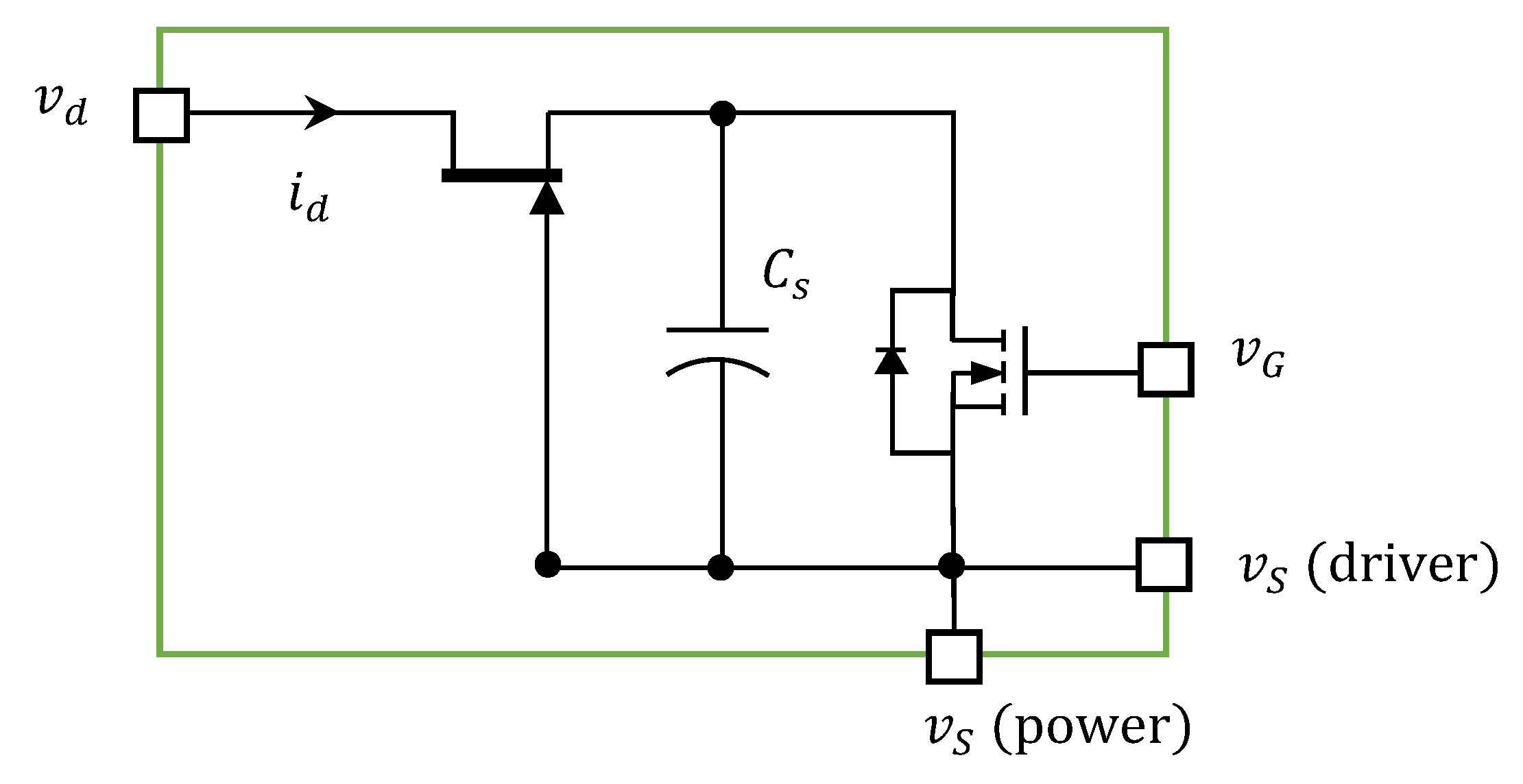
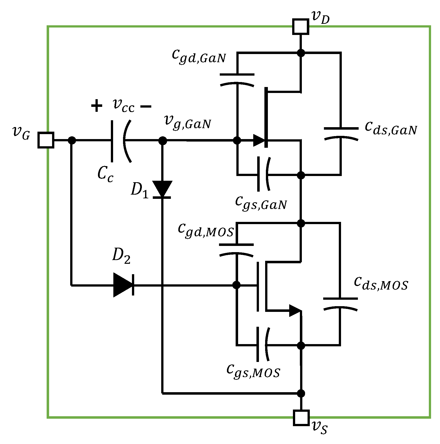
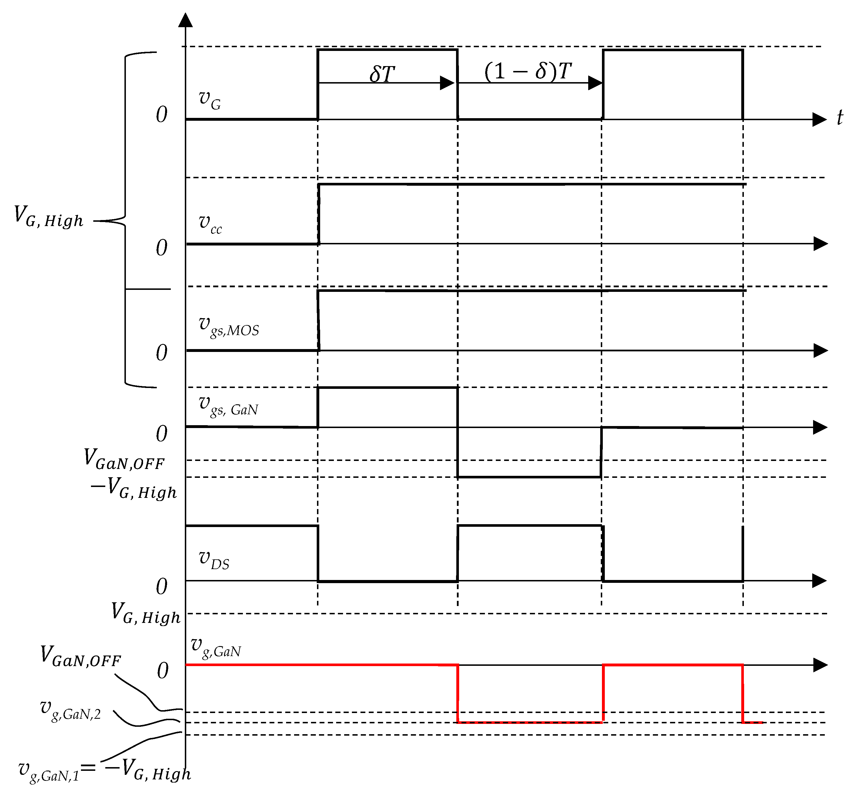
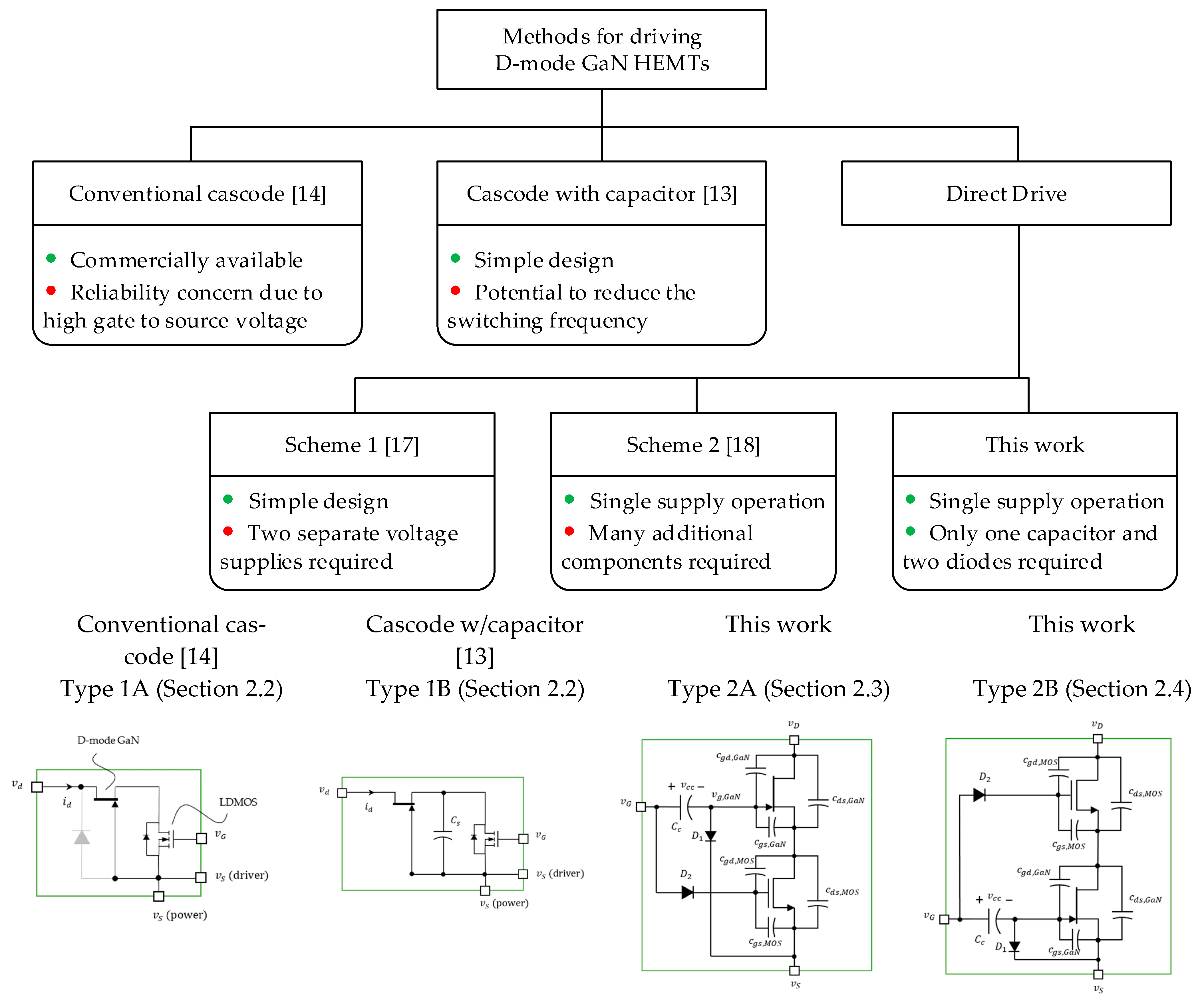
2. Cascode GaN HEMT Power Module
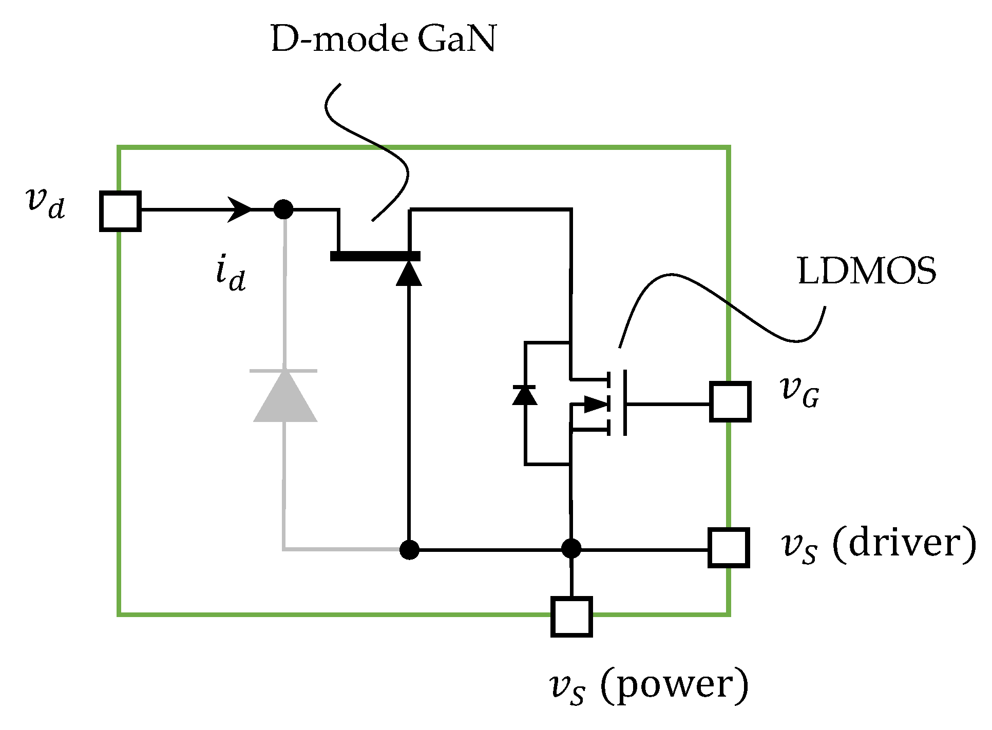
2.1. D-Mode GaN HEMT
2.2. MOS-Switching Cascode GaN HEMT
- Normally off; most of switching power supplies, such as flyback converter require this feature;
- Low Miller effect versus MOSFET; high switching frequency;
- Current limiting: the saturation current is constant with drain voltage because GaN has a negative temperature coefficient; the current decreases due to decreased electron mobility.
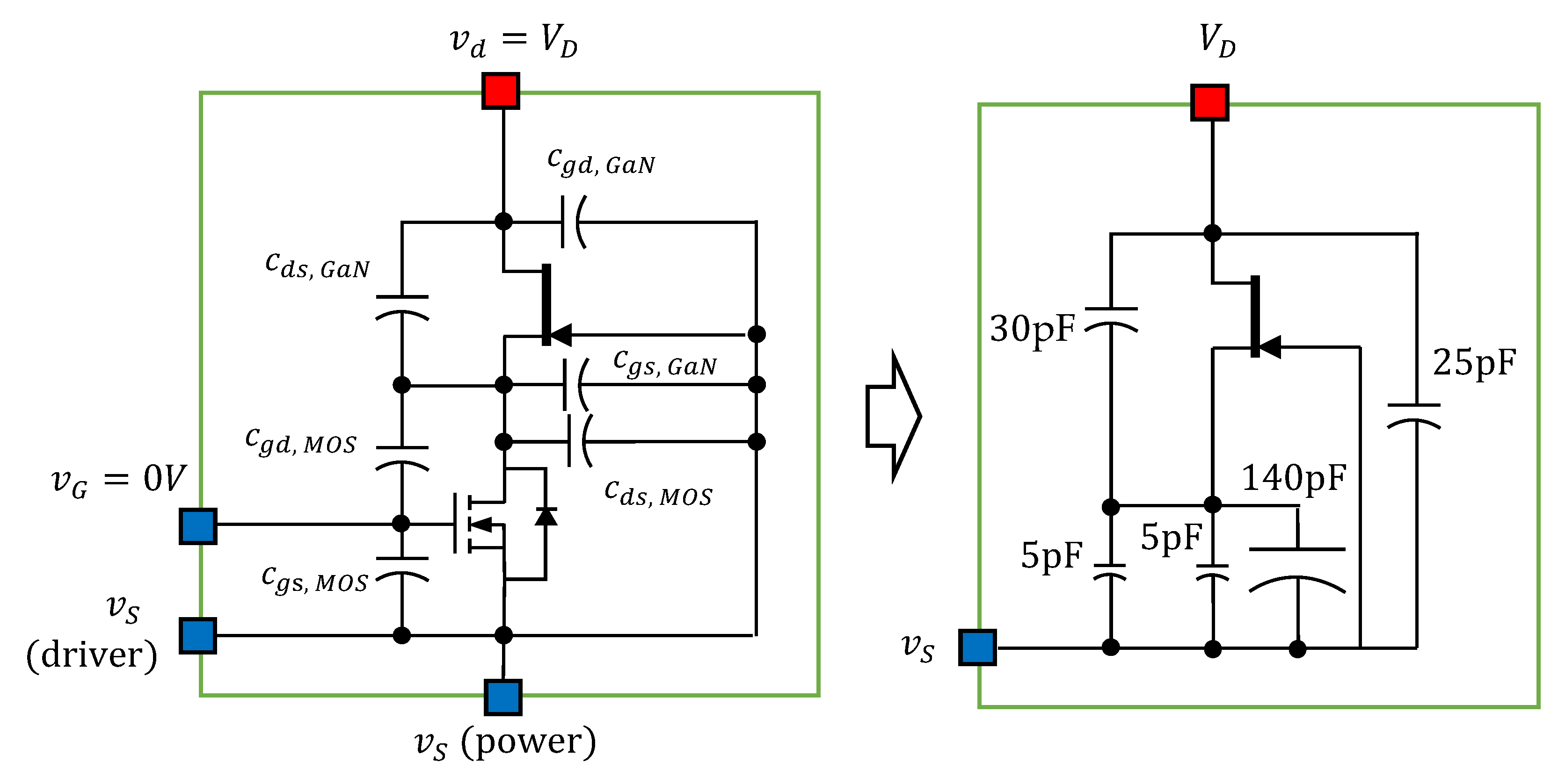
2.3. GaN-Switching Cascode GaN HEMT Power Module
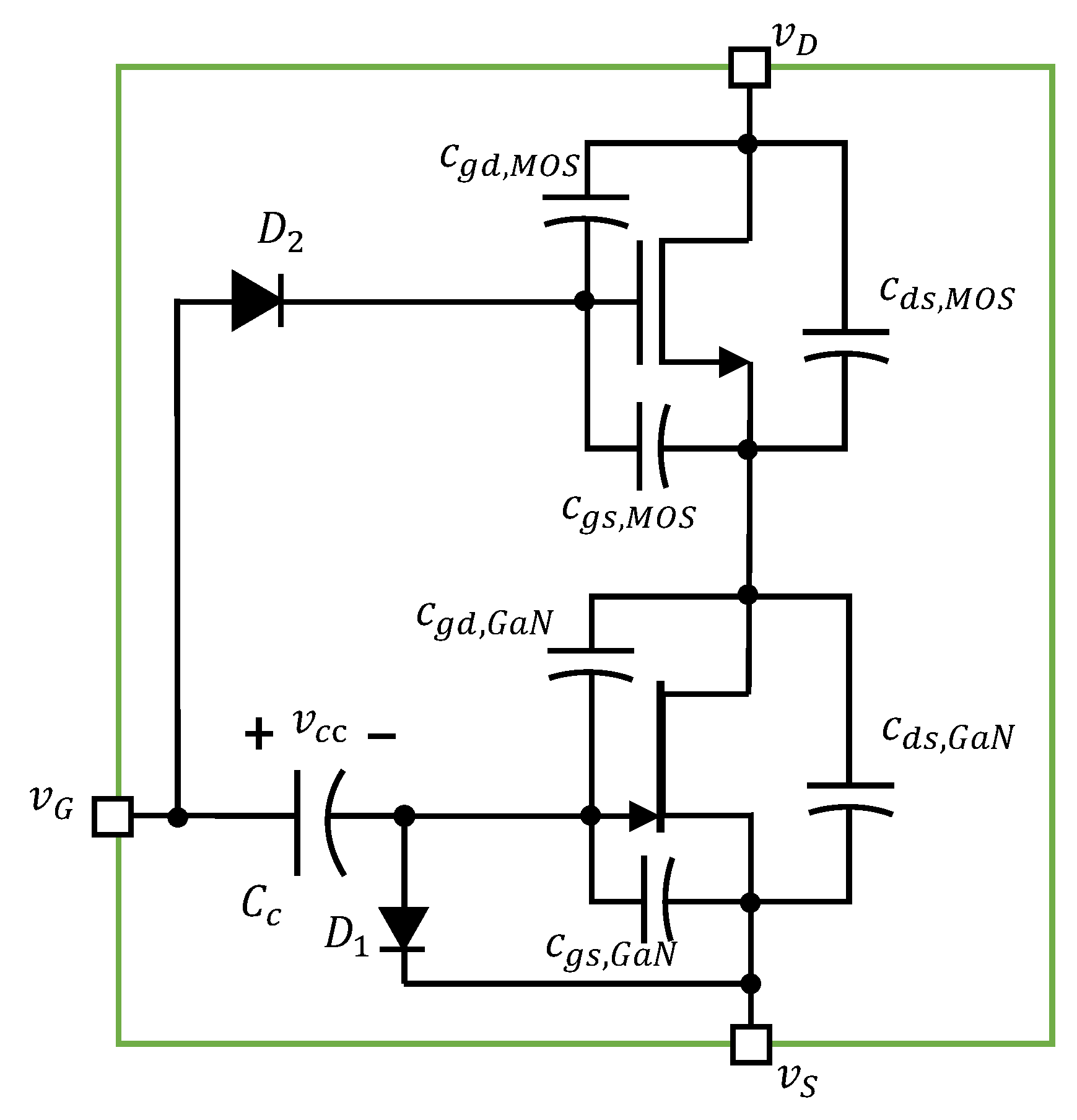
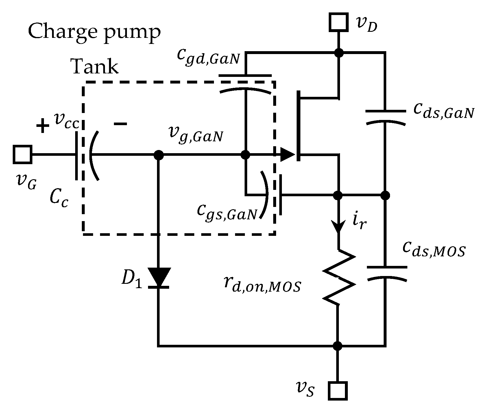
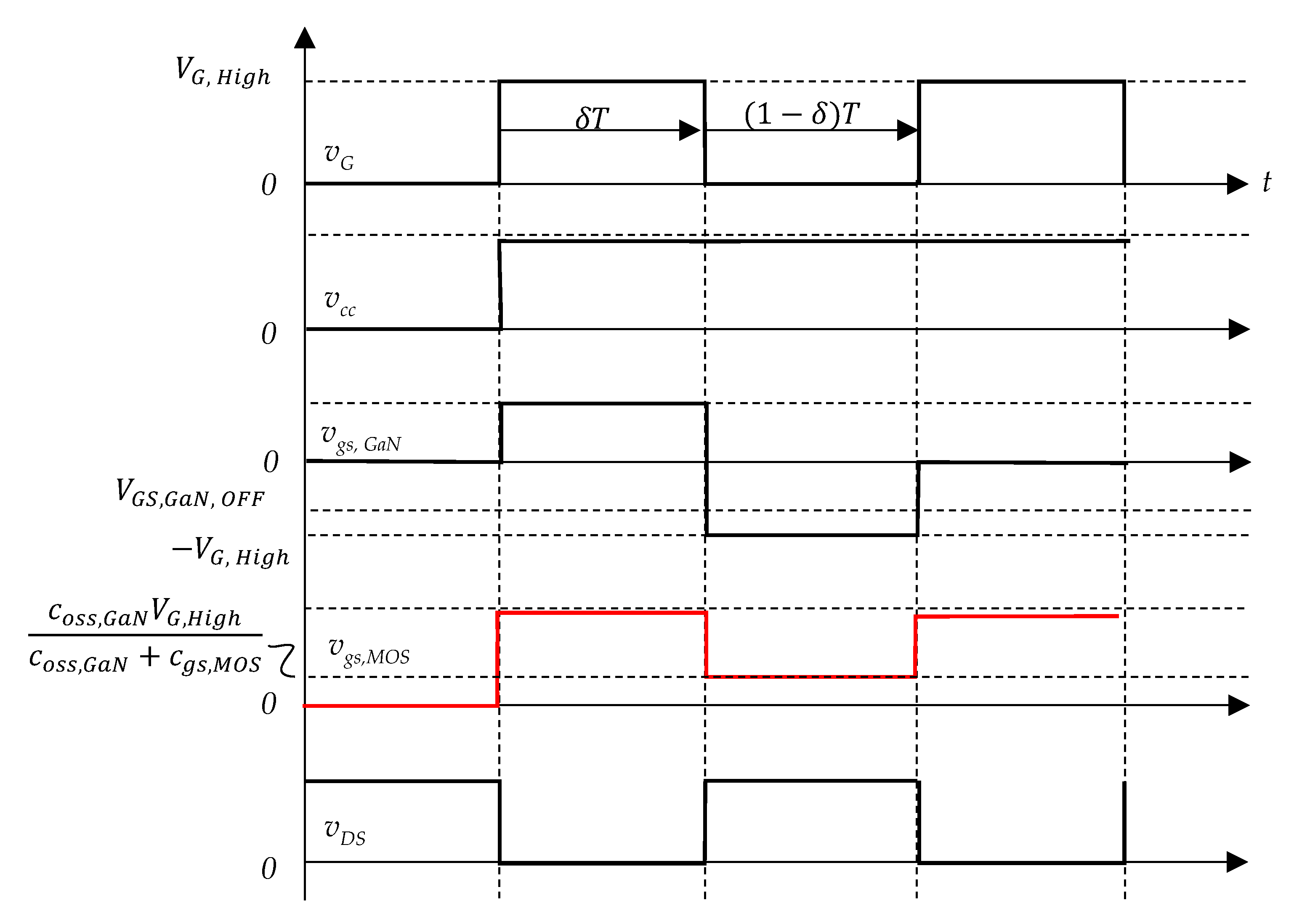
2.4. Alternative GaN-Switching Cascode GaN HEMT Power Module
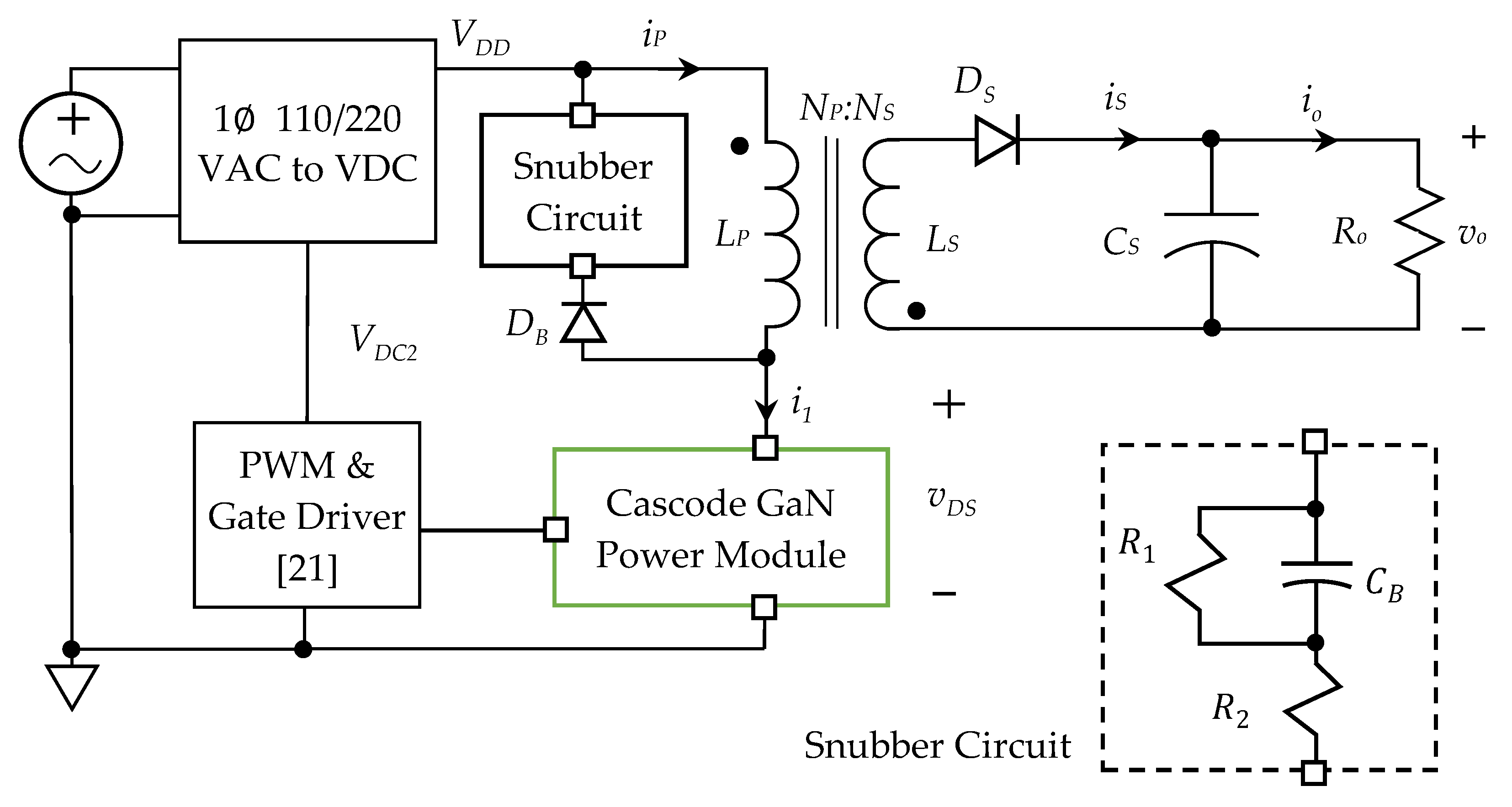
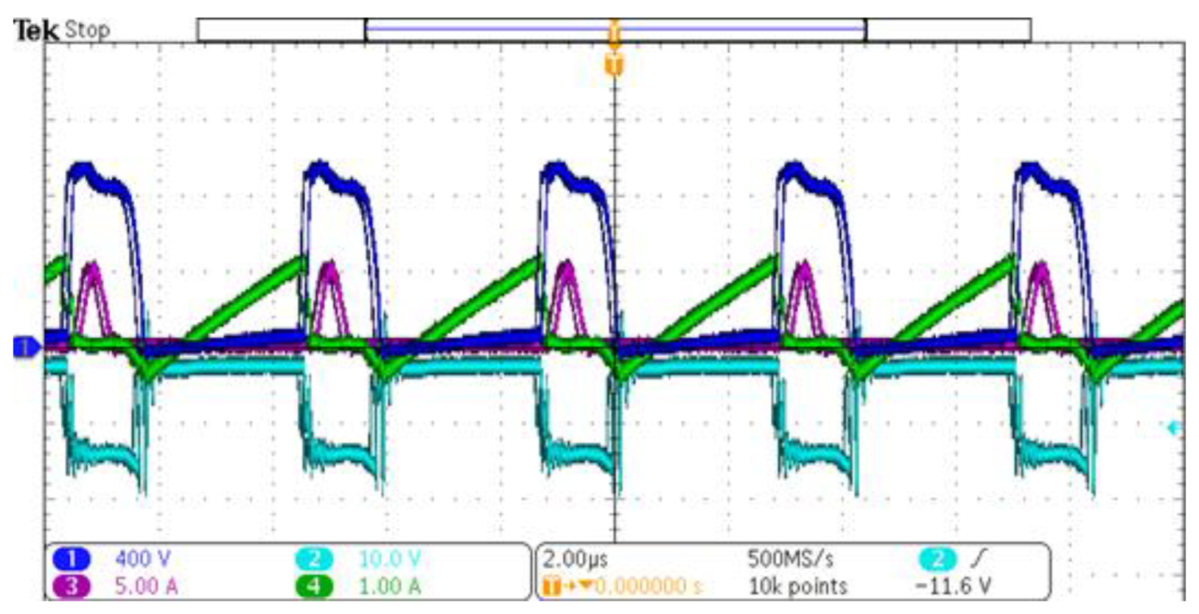
3. Flyback Converter
Continuous Current Mode (CCM) Analysis
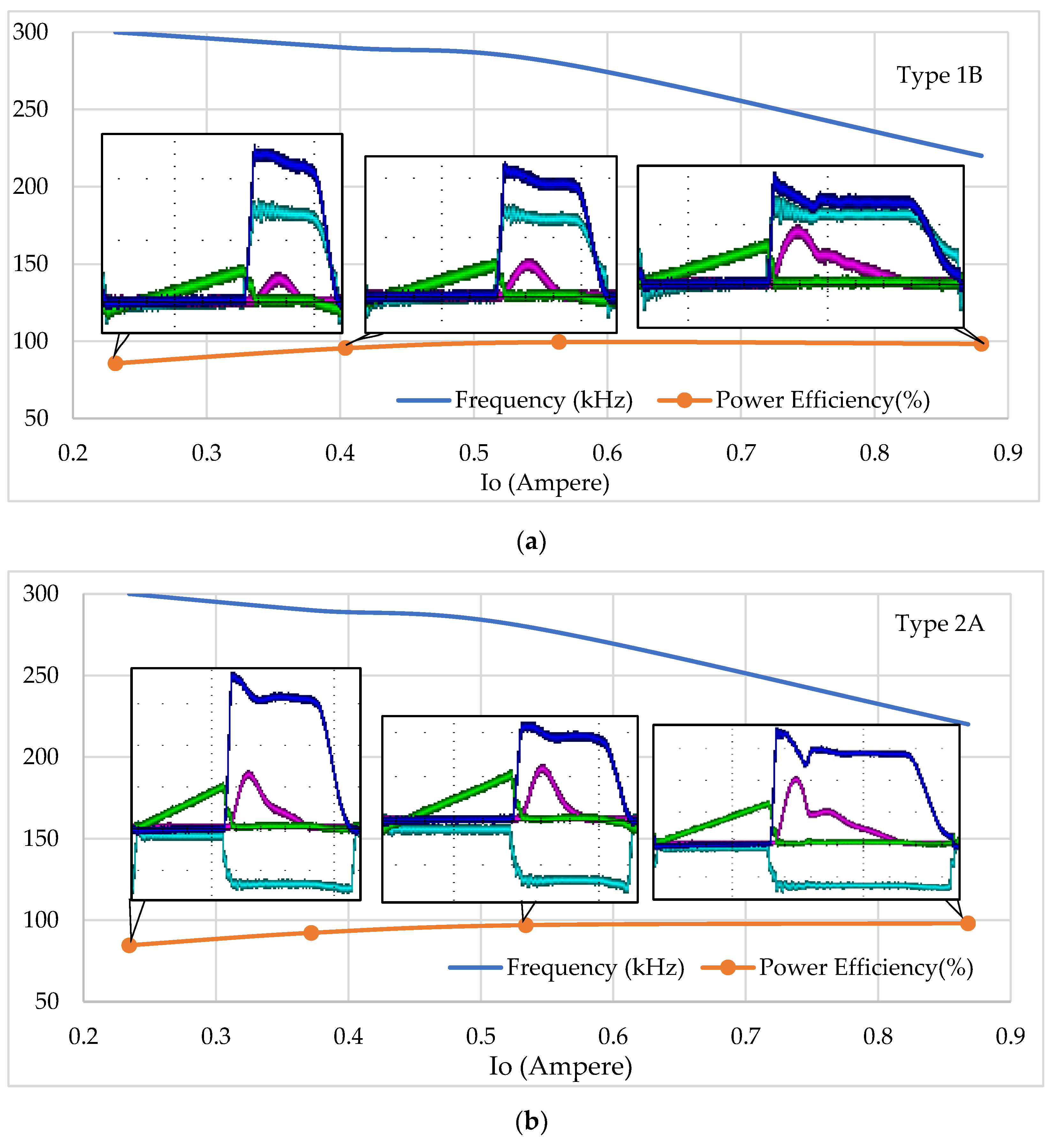
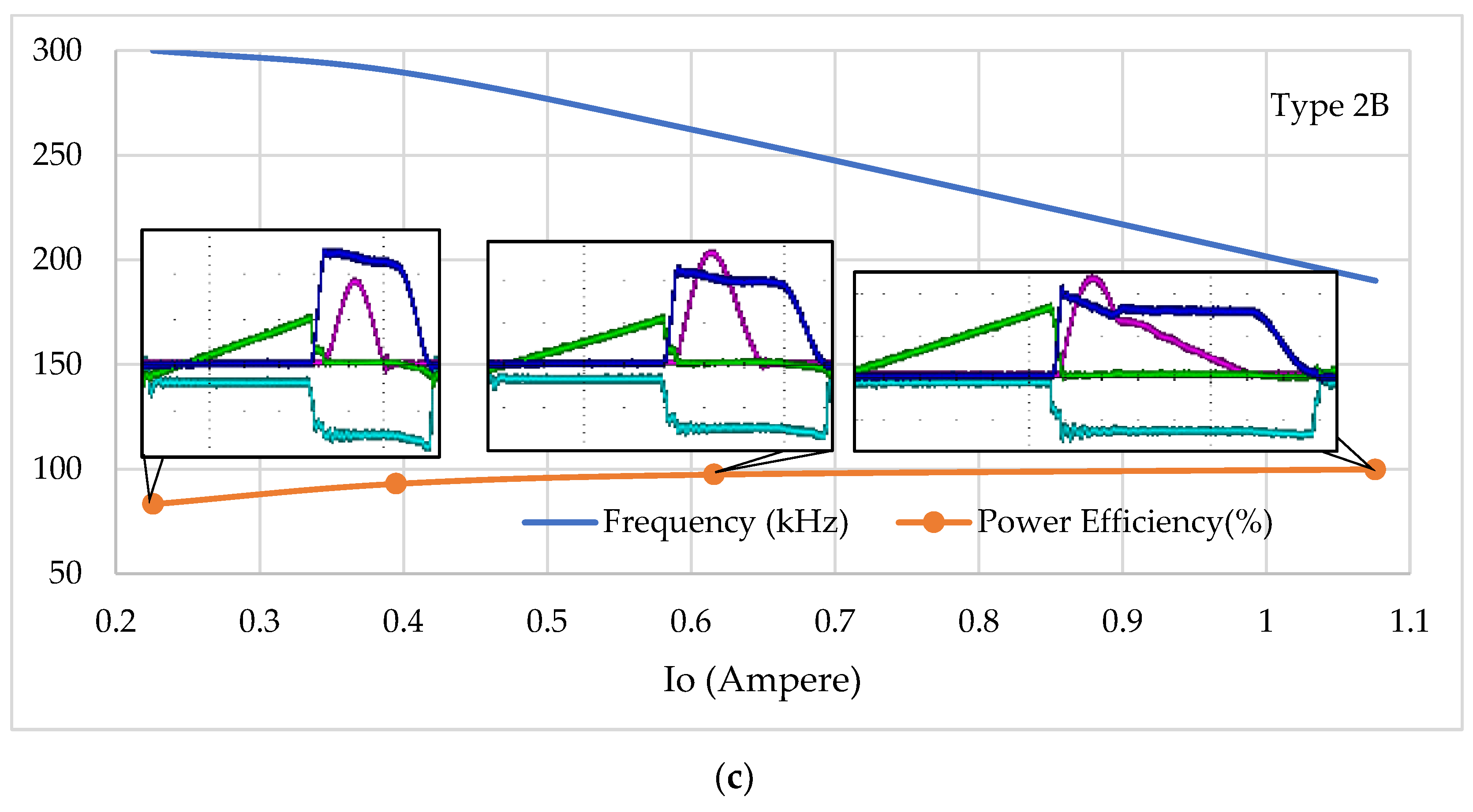
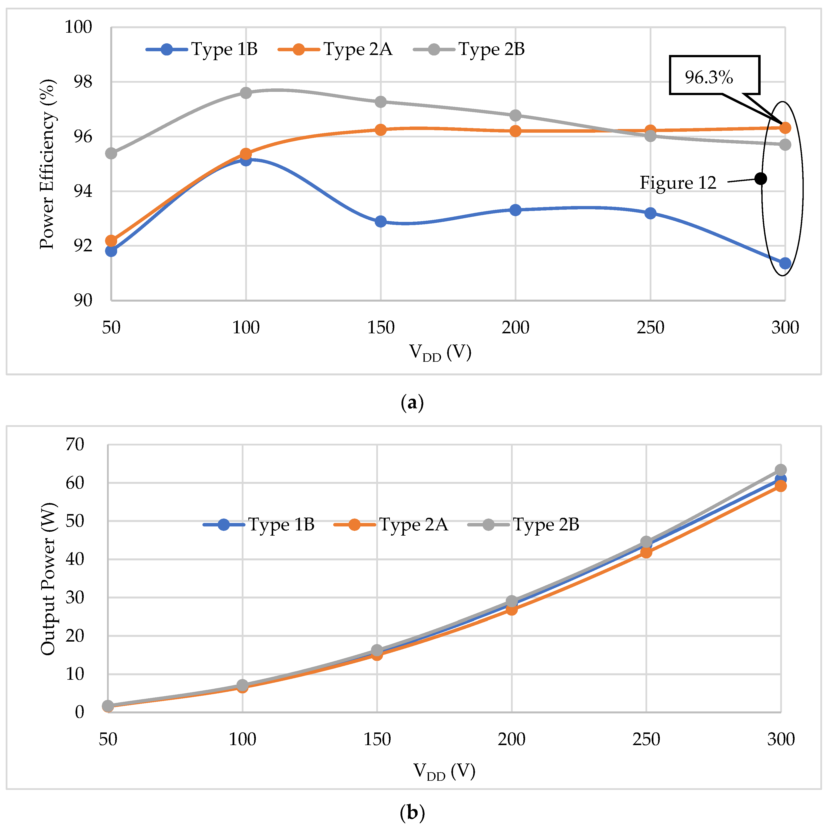
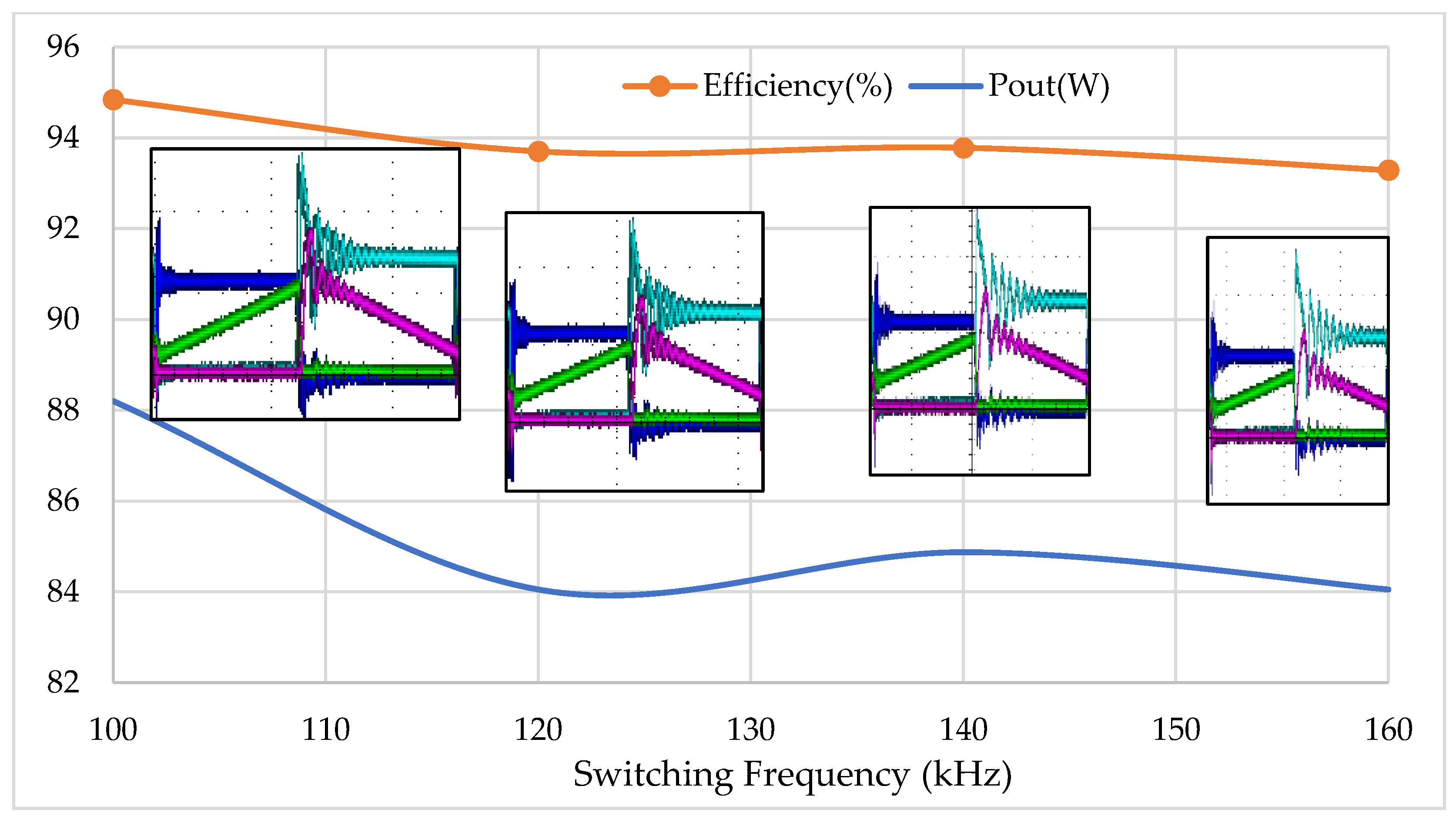
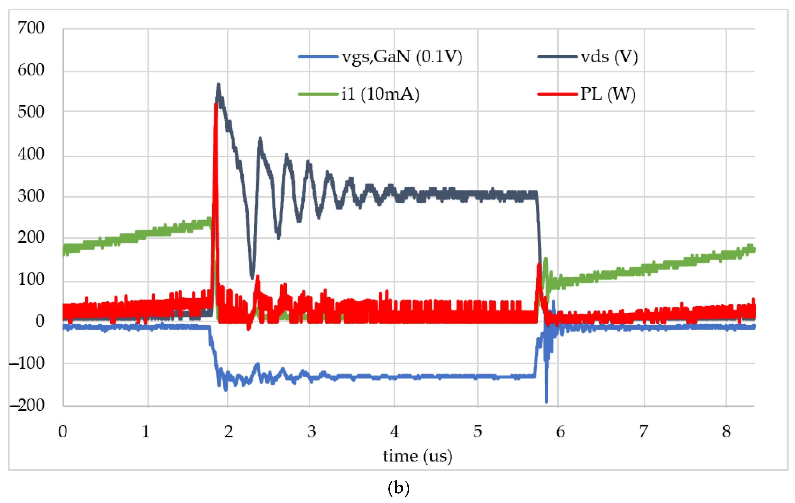
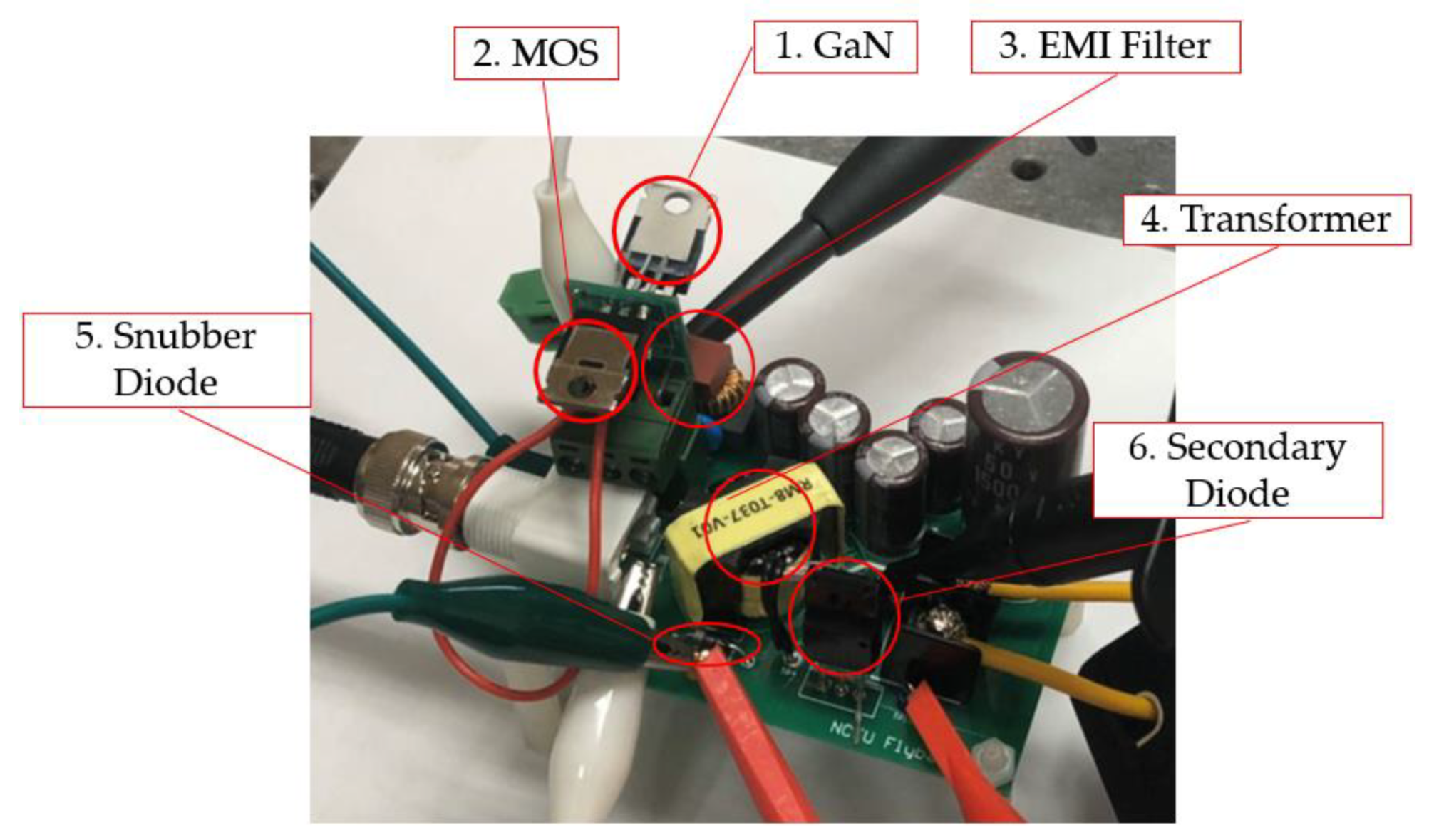
4. Results and Comparisons
5. Discussion
6. Conclusions
Author Contributions
Funding
Institutional Review Board Statement
Informed Consent Statement
Data Availability Statement
Acknowledgments
Conflicts of Interest
Nomenclature
| Symbol | Abbreviation |
| LP | inductance of primary winding |
| LS | inductance of secondary winding |
| k | coupling coefficient of transformer |
| a | turn ratio of transformer |
| cds | drain–source parasitic capacitance |
| coss | output parasitic capacitance |
| vDS | drain–source voltage of the power module |
| CB | snubber capacitance of flyback converter |
| DS | diode on secondary winding of flyback converter |
| DB | diode of the snubber of flyback converter |
| fs | switching frequency of flyback converter |
| δ | duty cycle of the switching of flyback converter |
| Co | output capacitance of flyback converter |
| Ro | output resistance of flyback converter |
| vDS,off | drain–source voltage when power module turns off |
| vG,High | gate voltage to turn power module on |
| VGS,GaN,OFF | the voltage required to turn D-mode GaN HEMT off |
| cgd | gate-drain parasitic capacitance |
| i1 | drain current of power module |
| ir | current leakage |
| iP | primary winding current |
| iS | secondary winding current |
| CC | charge pump capacitor |
| QC | the charge on the clamp capacitor |
| vds,ss | the steady state drain–source voltage |
| NP | primary turns of the transformer |
| NS | secondary turns of the transformer |
| PL,D2 | diode loss |
| PL,on | on-resistance loss of the transformer |
| PL,switching | switching loss of the transformer |
| CISS | input parasitic capacitance |
| Cjo | diode capacitance |
| CS | compensation capacitor of type 1B |
| tr | switch-off time of the power module |
| RoB | the boundary resistance between CCM and DCM |
| the ringing factor on the drain–source voltage during the transistor turns off | |
| Po | output power |
| PL | power loss |
| power efficiency |
References
- Chen, K.J.; Haberlen, O.; Lidow, A.; Tsai, C.L.; Ueda, T.; Uemoto, Y.; Wu, Y. GaN-on-Si Power Technology: Devices and Applications. IEEE Trans. Electron Devices 2017, 64, 779–795. [Google Scholar] [CrossRef]
- Ji, S.; Reusch, D.; Lee, F.C. High-Frequency High Power Density 3-D Integrated Gallium-Nitride-Based Point of Load Module Design. IEEE Trans. Power Electron. 2013, 28, 4216–4226. [Google Scholar] [CrossRef]
- Waradzyn, Z.; Stala, R.; Mondzik, A.; Skała, A.; Penczek, A. GaN-Based DC-DC Resonant Boost Converter with Very High Efficiency and Voltage Gain Control. Energies 2020, 13, 6403. [Google Scholar] [CrossRef]
- Jones, E.A.; Wang, F.F.; Costinett, D. Review of Commercial GaN Power Devices and GaN-Based Converter Design Challenges. IEEE J. Emerg. Sel. Top. Power Electron. 2016, 4, 707–719. [Google Scholar] [CrossRef]
- Liu, Z.; Lee, F.C.; Li, Q.; Yang, Y. Design of GaN-Based MHz Totem-Pole PFC Rectifier. IEEE J. Emerg. Sel. Top. Power Electron. 2016, 4, 799–807. [Google Scholar] [CrossRef]
- Zhang, W.; Wang, F.; Costinett, D.J.; Tolbert, L.M.; Blalock, B.J. Investigation of Gallium Nitride Devices in High-Frequency LLC Resonant Converters. IEEE Trans. Power Electron. 2017, 32, 571–583. [Google Scholar] [CrossRef]
- Ren, R.; Liu, B.; Jones, E.A.; Wang, F.F.; Zhang, Z.; Costinett, D. Capacitor-Clamped, Three-Level GaN-Based DC-DC Converter with Dual Voltage Outputs for Battery Charger Applications. IEEE J. Emerg. Sel. Top. Power Electron. 2016, 4, 841–853. [Google Scholar] [CrossRef]
- Sarkar, A.; Vankayalapati, B.T.; Anand, S. GaN Based Multiple Output Flyback Converter with Independently Controlled Outputs. IEEE Trans. Ind. Electron. 2021. [Google Scholar] [CrossRef]
- Karakaya, F.; Gülsuna, Ö.; Keysan, O. Feasibility of Quasi-Square-Wave Zero-Voltage-Switching Bi-Directional DC/DC Converters with GaN HEMTs. Energies 2021, 14, 2867. [Google Scholar] [CrossRef]
- Gurpinar, E.; Castellazzi, A. Tradeoff Study of Heat Sink and Output Filter Volume in a GaN HEMT Based Single-Phase Inverter. IEEE Trans. Power Electron. 2018, 33, 5226–5239. [Google Scholar] [CrossRef] [Green Version]
- Lidow, A.; de Rooij, M.; Strydom, J.; Reusch, D.; Glaser, J. GaN Transistors for Efficient Power Conversion, 3rd ed.; John Wiley & Sons: New York, NY, USA, 2019. [Google Scholar] [CrossRef]
- Zhang, W.; Huang, X.; Liu, Z.; Lee, F.C.; She, S.; Du, W.; Li, Q. A New Package of High-Voltage Cascode Gallium Nitride Device for Megahertz Operation. IEEE Trans. Power Electron. 2016, 31, 1344–1353. [Google Scholar] [CrossRef]
- Huang, X.; Du, W.; Lee, F.C.; Li, Q.; Liu, Z. Avoiding Si MOSFET Avalanche and Achieving Zero-Voltage Switching for Cascode GaN Devices. IEEE Trans. Power Electron. 2016, 31, 593–600. [Google Scholar] [CrossRef]
- Huang, X.; Liu, Z.; Li, Q.; Lee, F.C. Evaluation and Application of 600 v GaN HEMT in Cascode Structure. IEEE Trans. Power Electron. 2014, 29, 2453–2461. [Google Scholar] [CrossRef]
- Le, P.T.; Young, A. Cascode Semiconductor Package and Related Methods. U.S. Patent US9496207B1, 15 November 2016. [Google Scholar]
- Huang, X.; Du, W.; Lee, F.C.; Li, Q.; Zhang, W. Avoiding Divergent Oscillation of a Cascode GaN Device under High-Current Turn-Off Condition. IEEE Trans. Power Electron. 2017, 32, 593–601. [Google Scholar] [CrossRef]
- Zojer, B. A New Driving Concept for Normally-on GaN Switches in Cascode Configuration. In Proceedings of the Conference Proceedings—IEEE Applied Power Electronics Conference and Exposition (APEC), Long Beach, CA, USA, 20–24 March 2016; pp. 996–1001. [Google Scholar] [CrossRef]
- Wen, Y.; Rose, M.; Fernandes, R.; van Otten, R.; Bergveld, H.J.; Trescases, O. A Dual-Mode Driver IC with Monolithic Negative Drive-Voltage Capability and Digital Current-Mode Controller for Depletion-Mode GaN HEMT. IEEE Trans. Power Electron. 2017, 32, 423–432. [Google Scholar] [CrossRef]
- Wu, C.-C.; Liu, C.-Y.; Wang, G.-B.; Shieh, Y.-T.; Chieng, W.-H.; Chang, E.Y. A New GaN-Based Device, P-Cascode GaN HEMT, and Its Synchronous Buck Converter Circuit Realization. Energies 2021, 14, 3477. [Google Scholar] [CrossRef]
- Weng, Y.C.; Wu, C.C.; Chang, E.Y.; Chieng, W.H. Minimum Power Input Control for Class-E Amplifier Using Depletion-Mode Gallium Nitride High Electron Mobility Transistor. Energies 2021, 14, 2302. [Google Scholar] [CrossRef]
- Tang, L.C.; Jeng, S.L.; Chang, E.Y.; Chieng, W.H. Variable-Frequency Pulse Width Modulation Circuits for Resonant Wireless Power Transfer. Energies 2021, 14, 3656. [Google Scholar] [CrossRef]
- Kumar, R.; Wu, C.C.; Liu, C.Y.; Hsiao, Y.L.; Chieng, W.H.; Chang, E.Y. Discontinuous Current Mode Modeling and Zero Current Switching of Flyback Converter. Energies 2021, in press. [Google Scholar]


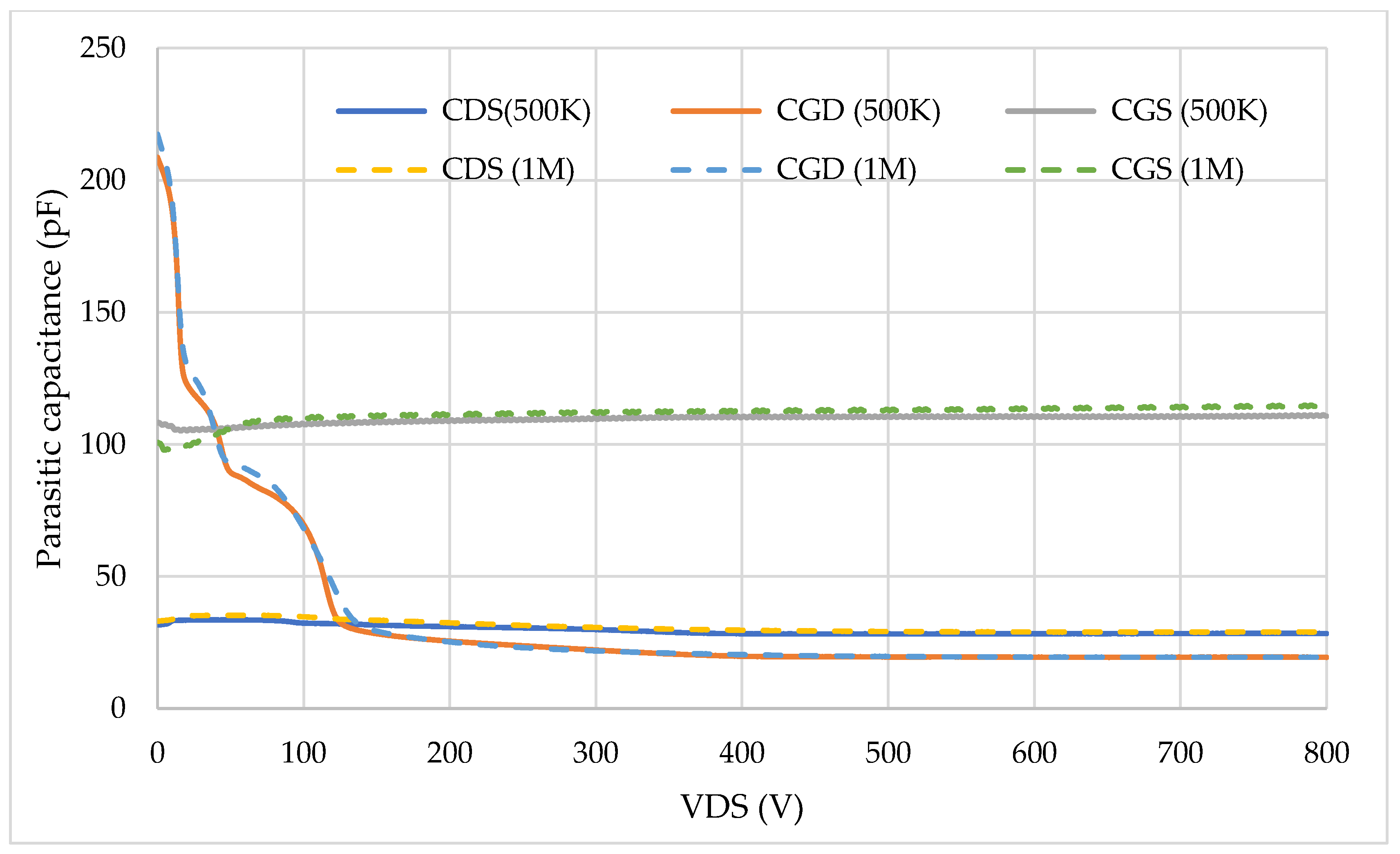
| Symbol | Unit | Description | Value | vDS | ||
|---|---|---|---|---|---|---|
| 0 V | 200 V | 800 V | ||||
| vGS,ON vGS,OFF | V | Turn-on voltage (All) | −7 | |||
| CDS | pF | Parasitic capacitance | 40 | 33 | 30 | |
| CGD | pF | Parasitic capacitance | 220 | 26 | 20 | |
| CGS | pF | Parasitic capacitance | 100 | 112 | 115 | |
| VGS,max | V | Maximum gate–source voltage | 8 | |||
| VGS,min | V | Minimum gate–source voltage | −30 | |||
| VDS,BD | V | Drain–source breakdown voltage | 800 | |||
| Symbol | Unit | Description | Value |
|---|---|---|---|
| Cs | nF | Compensation capacitor of Type 1B | 1 |
| NMOS | E-mode N channel MOSFET | IRF610 |
| Symbol | Unit | Description | Value |
|---|---|---|---|
| Cc | nF | Charge pump capacitor of Type 2x | 10 |
| NMOS | E-mode N channel MOSFET | IRF610 | |
| cgs,NMOS | pF | Parasitic gate–source capacitance of NMOS | 200 |
| D1 | Low Leakage diode | BAV170 | |
| D2 | General purpose diode | 1N4007 |
| Symbol | Unit | Description | Value |
|---|---|---|---|
| LP | uH | primary inductance of transformer | 400 |
| LS | uH | secondary inductance of transformer | 10.27 |
| a | turn ratio of transformer | 6.24 | |
| k | coupling coefficient of transformer | 98.7% | |
| CB | nF | capacitance of the snubber | 1 |
| R2 | Ω | series resistance of the snubber | 33 |
| R1 | kΩ | parallel resistance of the snubber | 100 |
| CS | uF | capacitor on secondary side | 2200 |
| Cjo | pF | capacitance of the diodes | 10 |
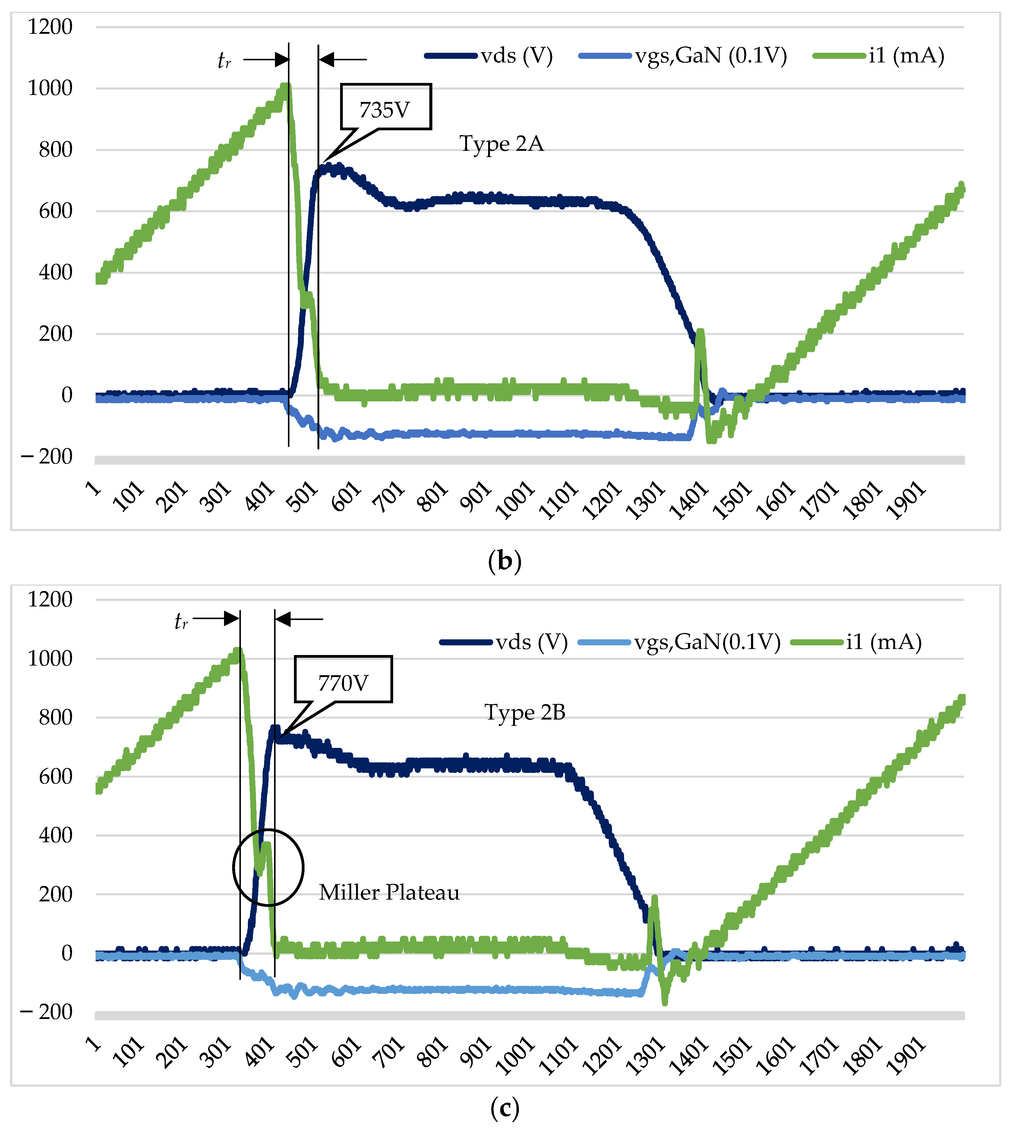
| Symbol | Unit | Description | Type 1B | Type 2A | Type 2B |
|---|---|---|---|---|---|
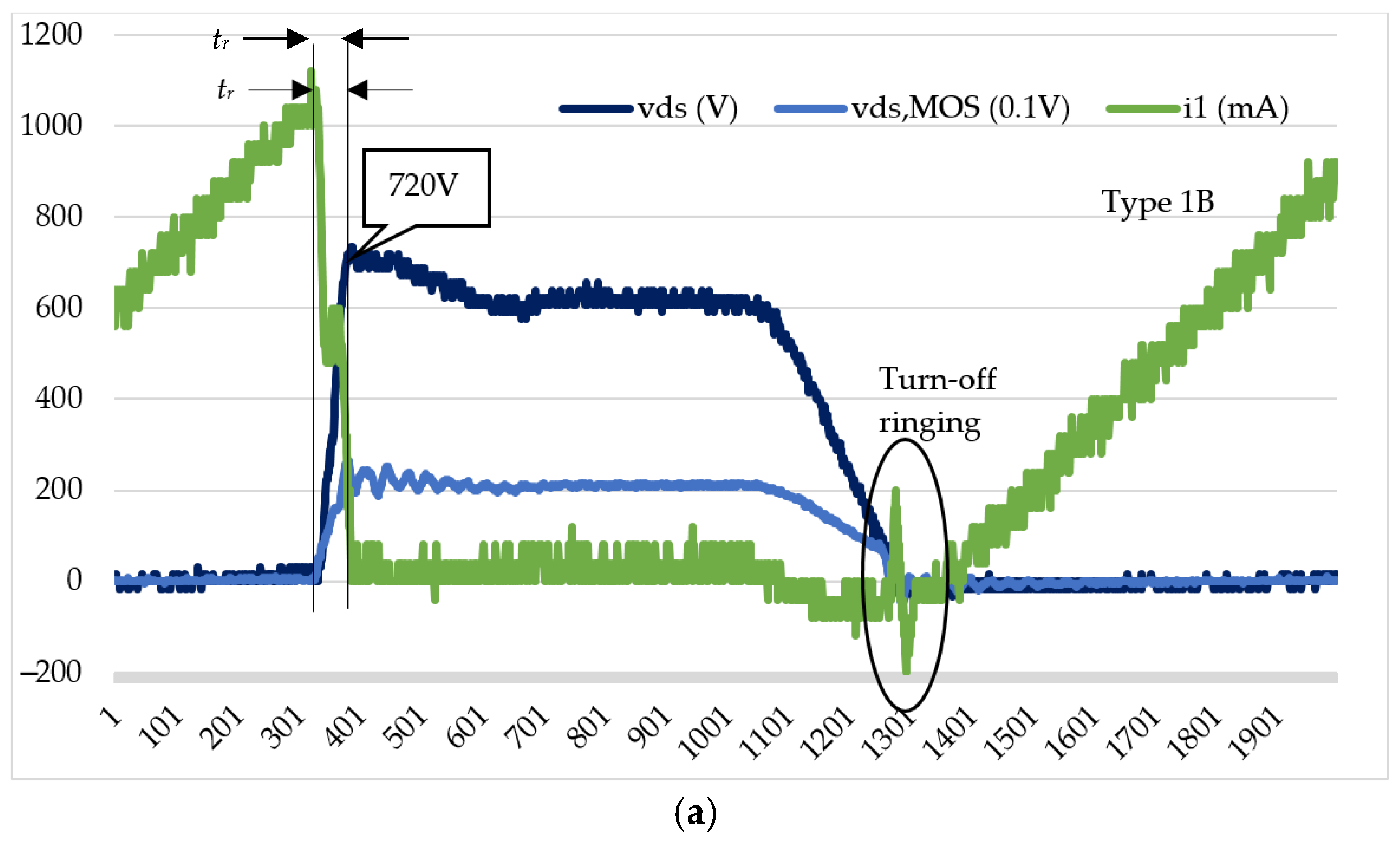
| tr | ns | switch-off time | 164 | 170 | 188 |
| vds,max | V | Max. drain–source voltage | 720 | 735 | 770 |
| Coss | pF | Estimated output parasitic capacitance using Equation (16) | 170 | 183 | 233 |
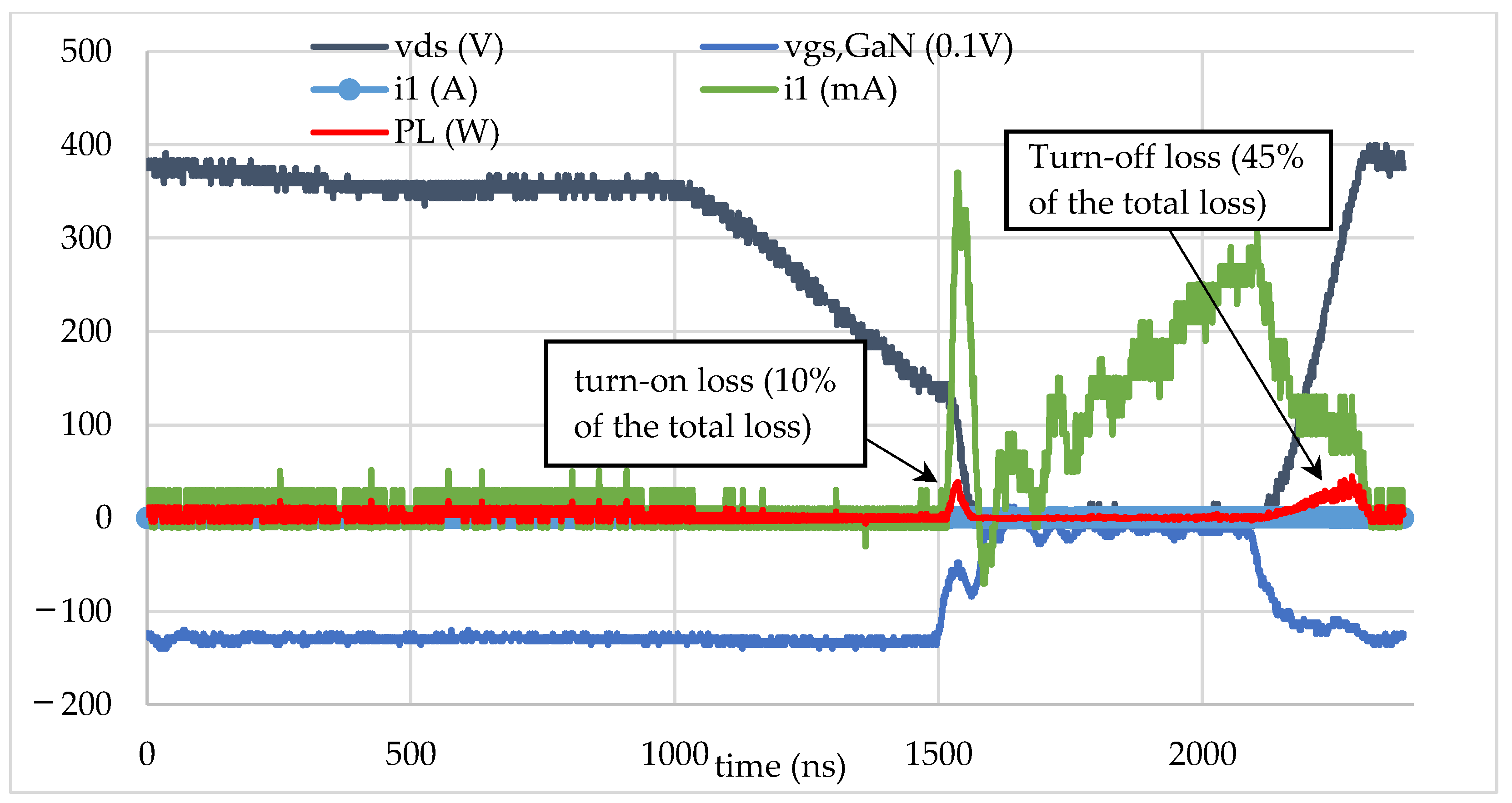
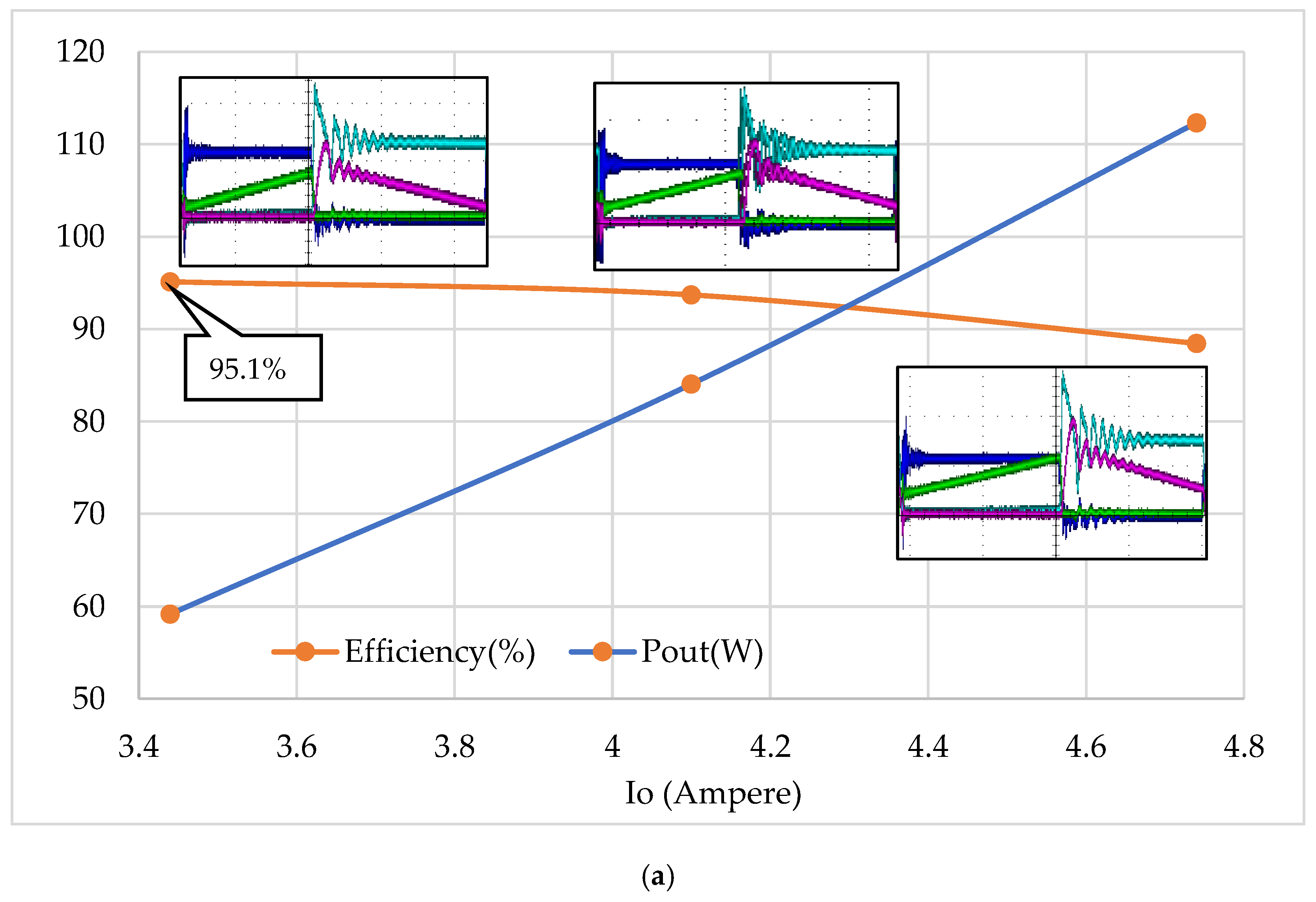
| Mode | Efficiency (%) | Pout (W) | Duty (%) | VDD (V) | Ro Ω | vds,max (V) | vds,ss * | Io,max (A) | Vo (V) |
|---|---|---|---|---|---|---|---|---|---|
| DCM | 96.3 | 59.62 | 48 | 300 | 50 | 735 | 641 | 6.9 | 54.6 |
| CCM | 95.1 | 59.17 | 43 | 150 | 5 | 423 | 257 | 35.4 | 17.2 |
| Io | δ (%) | i1,min | ∆i1 | ||
|---|---|---|---|---|---|
| Equation (29) | Experiment | Equation (14) | Experiment | ||
| 33.44 | 43 | 0.35 | 0.34 | 1.34 | 1.26 |
| 4.1 | 48 | 0.62 | 0.6 | 1.5 | 1.4 |
| 4.74 | 53 | 1.02 | 0.88 | 1.66 | 1.52 |
Publisher’s Note: MDPI stays neutral with regard to jurisdictional claims in published maps and institutional affiliations. |
© 2021 by the authors. Licensee MDPI, Basel, Switzerland. This article is an open access article distributed under the terms and conditions of the Creative Commons Attribution (CC BY) license (https://creativecommons.org/licenses/by/4.0/).
Share and Cite
Wu, C.-C.; Liu, C.-Y.; Anand, S.; Chieng, W.-H.; Chang, E.-Y.; Sarkar, A. Comparisons on Different Innovative Cascode GaN HEMT E-Mode Power Modules and Their Efficiencies on the Flyback Converter. Energies 2021, 14, 5966. https://doi.org/10.3390/en14185966
Wu C-C, Liu C-Y, Anand S, Chieng W-H, Chang E-Y, Sarkar A. Comparisons on Different Innovative Cascode GaN HEMT E-Mode Power Modules and Their Efficiencies on the Flyback Converter. Energies. 2021; 14(18):5966. https://doi.org/10.3390/en14185966
Chicago/Turabian StyleWu, Chih-Chiang, Ching-Yao Liu, Sandeep Anand, Wei-Hua Chieng, Edward-Yi Chang, and Arnab Sarkar. 2021. "Comparisons on Different Innovative Cascode GaN HEMT E-Mode Power Modules and Their Efficiencies on the Flyback Converter" Energies 14, no. 18: 5966. https://doi.org/10.3390/en14185966
APA StyleWu, C.-C., Liu, C.-Y., Anand, S., Chieng, W.-H., Chang, E.-Y., & Sarkar, A. (2021). Comparisons on Different Innovative Cascode GaN HEMT E-Mode Power Modules and Their Efficiencies on the Flyback Converter. Energies, 14(18), 5966. https://doi.org/10.3390/en14185966