1. Introduction
Gallium nitride (GaN) High Electron Mobility Transistors (HEMTs) offer outstanding performance at high power and high switching frequency [
1], thanks to the material’s robust electrical and thermal properties. The fundamental GaN-HEMT is a depletion mode device (D-mode) also called Normally-ON, meaning that the device is in conduction mode at V
gs = 0 V. The reason for this is that the conduction channel (2DEG) is spontaneously present when the AlGaN/GaN or another barrier alloy is in contact with the GaN channel layer [
2]. For high power application and for safety reasons, the circuit designers need an enhancement mode device called Normally-OFF that can block the current at V
gs = 0 V, thanks to its positive pinch-off voltage (V
th). So, to shift the V
th from negative values to positive values, several approaches are investigated in the literature: (A) Fluorine (F
− ions) implantation in the upper part of the barrier layer to deplete the channel [
3]; (B) Gate recess on the barrier layer [
4]; (C) Etching of the barrier layer using an etch-stop layer [
5]; (D) p-doped GaN layer on top of the AlGaN barrier layer [
6]. This last approach is used in this paper. In the literature, the reported papers present a process where the p-doped GaN is grown in the same epitaxy with the HEMT active layer. During the device fabrication, this p-doped GaN layer is removed in the device access region using plasma etching and left only below the gate [
7]. The exposure of the access region to the plasma can degrade the device resistances and consequently increase the R
on [
8]. In this paper, we are investigating a new approach where the p-doped GaN is selectively re-grown on the AlGaN barrier layer using the CBE (Chemical Beam Epitaxy) technique. Using this approach, the device access region is not exposed to an etching plasma in subsequent step during the device fabrication process. The choice of the CBE technique is an attempt to leverage some of its advantages, such as outstanding selectivity, lower growth temperature compared to the standard MOVPE technique, and the tool compatibility with standard cluster tool technology.
Such an approach has never been reported in the literature and offers a good option to improve the high power HEMT device performance. To determine the appropriate p doping for our device, the Vth vs. the p doping level is investigated using the TCAD simulator (Silvaco). The device is also fabricated and characterized.
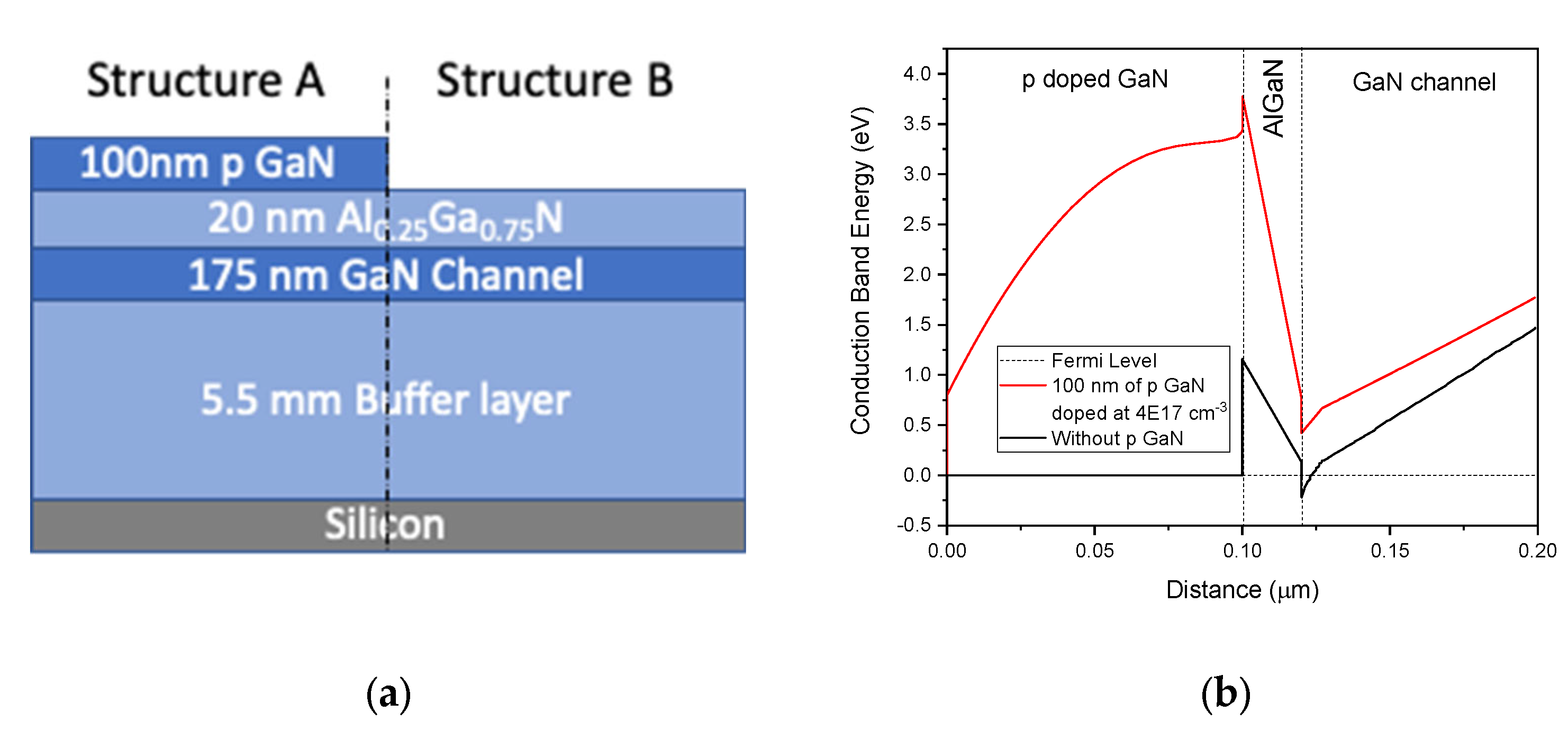
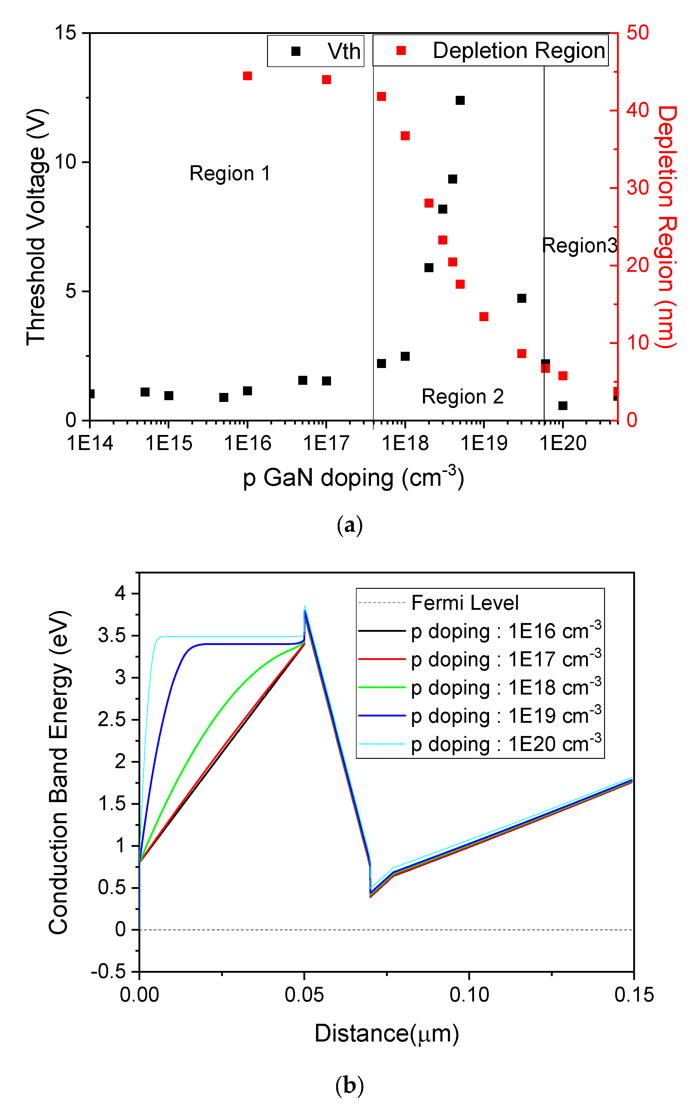
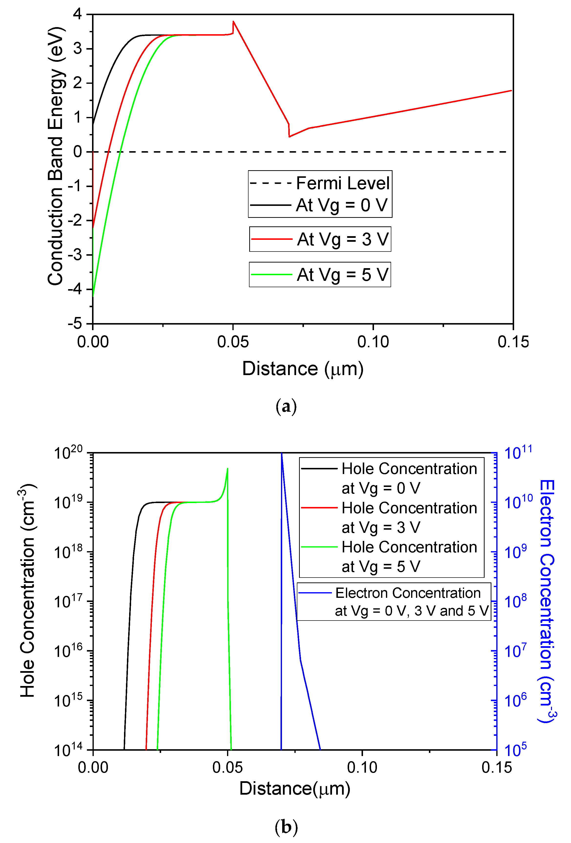
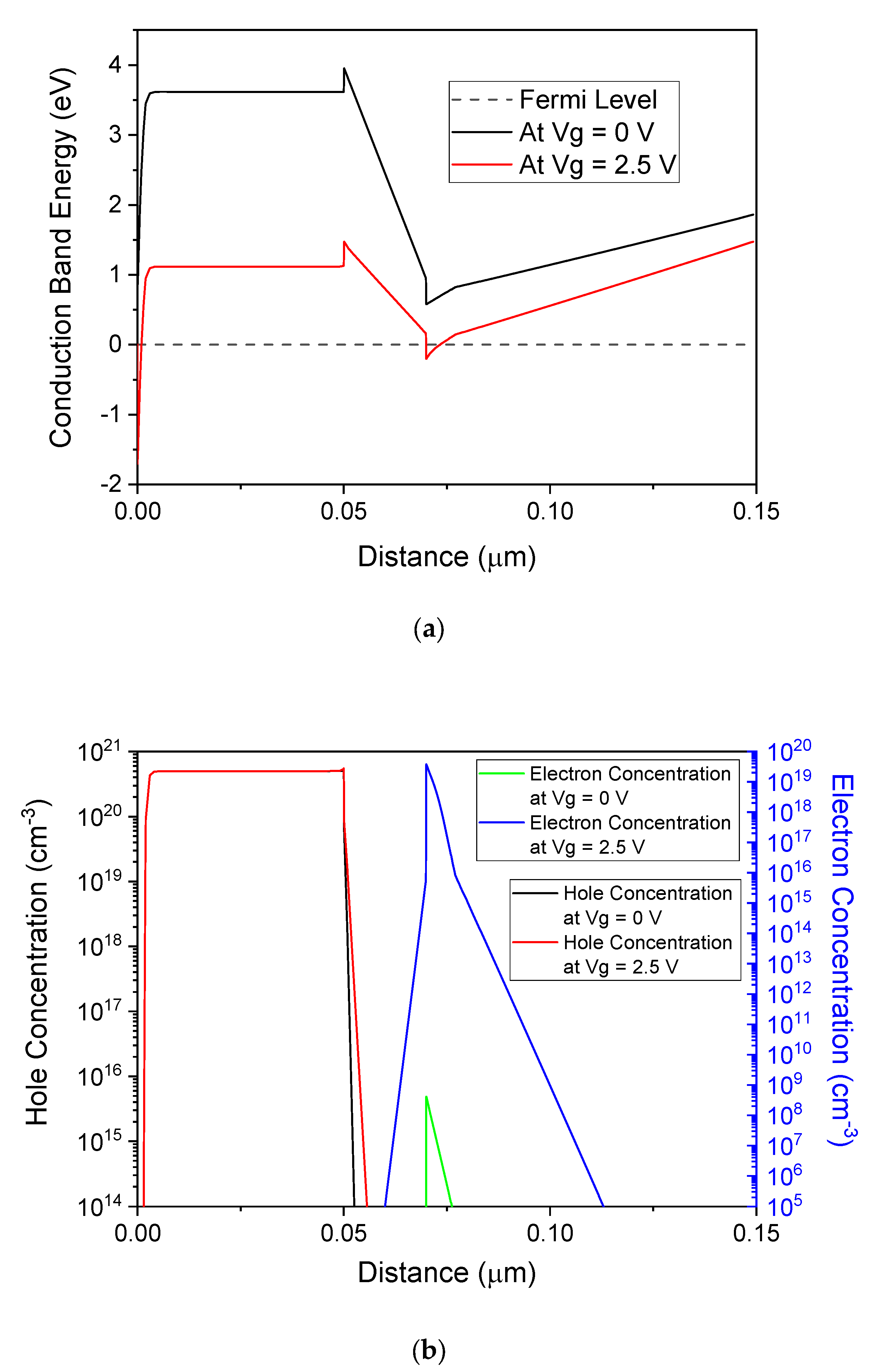
2. Simulation Results
To understand the effect of the p doping of the GaN layer on the device performance, TCAD simulation (Silvaco/Atlas) has been performed. Several works in the literature report on the same subject by giving an overview and brief explanation of the real effect of the p doping on the pinch-off voltage of the Normally-OFF HEMT device [
6,
9]. In this paper, we will take one further step for the understanding of such an effect by using the TCAD tool to explain the impact of the GaN p doping on the device physics.
For that purpose, two structures (
Figure 1a) were simulated, structure A (with p-doped GaN layer) and structure B (without p-doped GaN layer).
Figure 2 represents the architecture of the simulated device.
In
Figure 1b, the band diagram of the two structures is presented. For the 2D simulation to determine the pinch-off of the device, a 50 nm thick p-doped GaN layer is used instead of 100 nm. This is due to the simulator converging problem that appears when the p-doped GaN layer thickness is very thick. So, we decided to reduce the thickness of the p-doped GaN layer to 50 nm to help the simulator to converge correctly. Even if the thickness of this layer is different from that used in the fabricated devices, we can still see a certain similarity between the theoretical and the achieved results.
In
Figure 1b, we can observe that the p-doped GaN layer will lift-up the conduction band and then deplete the channel. Therefore, the fabricated device using structure A will be Normally-OFF, while the one using Structure B will be Normally-ON.
In
Figure 3 are presented the pinch-off voltage extracted at I
ds = 1 mA/mm @ V
ds = 10 V and the p-doped GaN layer depletion region thickness vs. the GaN p doping values. This depletion region is extracted for the hole density equal to 1E14 cm
−3 in the p-doped GaN layer. In this curve, we can observe three regions (
Figure 3):
Region 1: for p doping lower than 4E17 cm
−3, the gate contact is Schottky type. In this region, we can consider that the p-doped GaN layer is quasi-depleted at V
gs = 0 V as shown in
Figure 3b. Consequently, an important part of the gate voltage is directly applied to the channel and can easily switch on the device. In this region, the V
th is around 1 V.
Region 2: in this region, the p-doped GaN layer is partially depleted. The gate voltage, therefore, needs to first deplete the p-doped GaN layer and then it will have access to the channel to increase the electron density in the 2D electron gas. For doping in the 5E17–1E18 cm
−3 range, the un-depleted part of the p-doped GaN layer is relatively thin with less hole density; therefore, it requires less than 2V bias for total depletion. For this p doping range, the increase in the V
th is low. For higher p doping, full depletion of the p-doped GaN layer becomes more difficult, forcing an increase in V
th. This can be illustrated in
Figure 4. In
Figure 4a, for p-doping equal 1E19 cm
−3 and by varying V
gs from 0 to 5 V, as expected, the depletion region of the p-doped GaN layer becomes wider by increasing V
gs. At the same time, the conduction band and the electron density in the channel did not change (
Figure 4b). Consequently, the gate voltage only depletes the p-doped GaN layer and needs to deplete it completely to allow access to the channel. This can explain why the V
th is very high for the p doping around 1E
19 cm
−3.
Region 3: when the p GaN doping level starts to be high enough to stop the depletion region very close to the gate contact at V
gs = 0 V (
Figure 5), the tunneling phenomenon starts to take place through this thin layer and the Gate contact becomes ohmic instead of Schottky. In this region, the p-doped GaN layer will be equivalent to a gate serial resistance with no voltage consumption (negligeable) because the gate leakage current of the device is very low. Consequently, we can consider that the Vgs will be applied directly at the p-doped GaN/AlGaN interface. So, V
th decreases to a value comparable to, or even lower than the one achieved for low p doping levels in Region 1.
The p doping level in the fabricated device was 4E17 cm−3, producing a Vth of around 1.5 V.
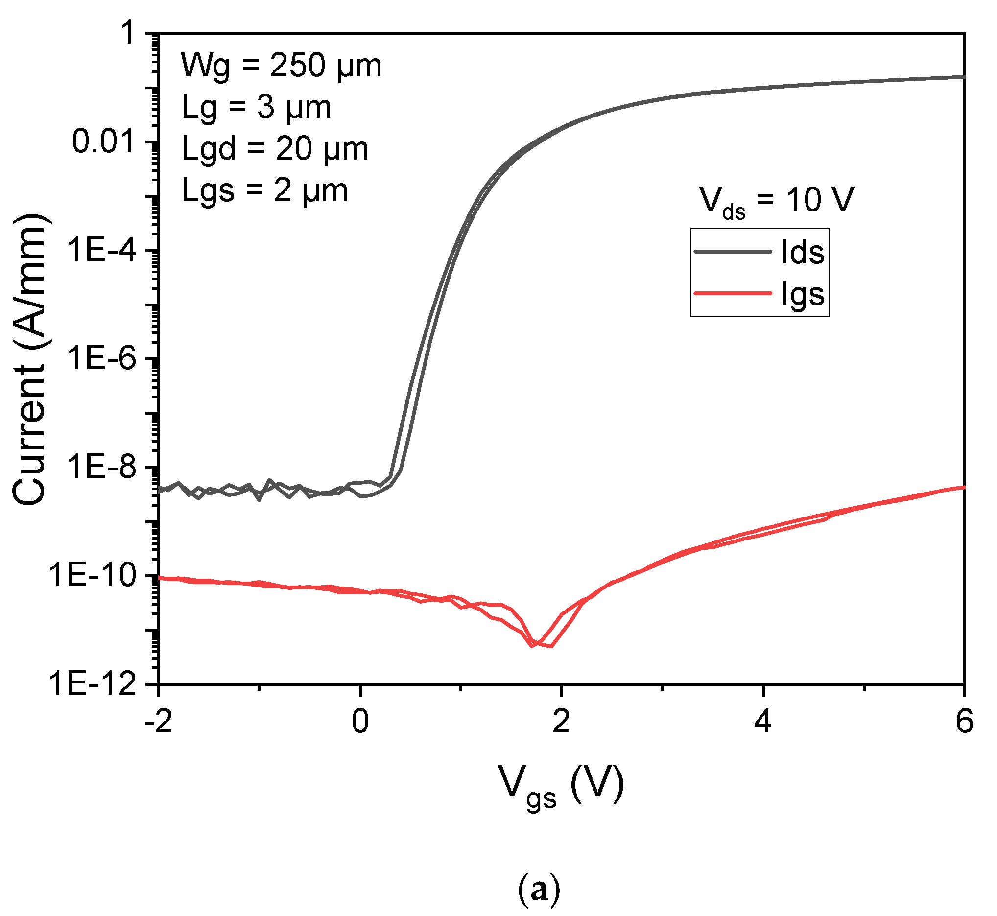
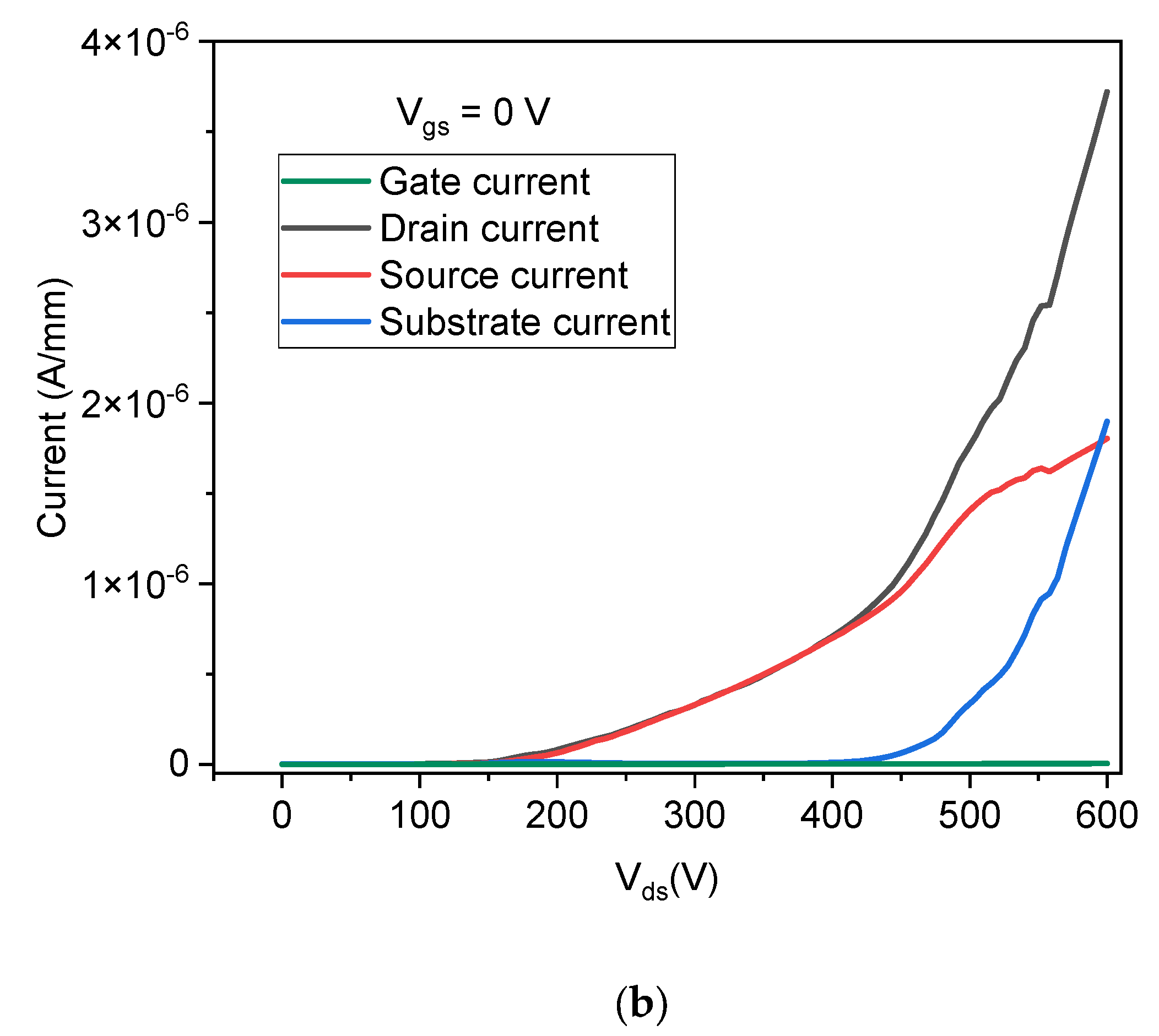
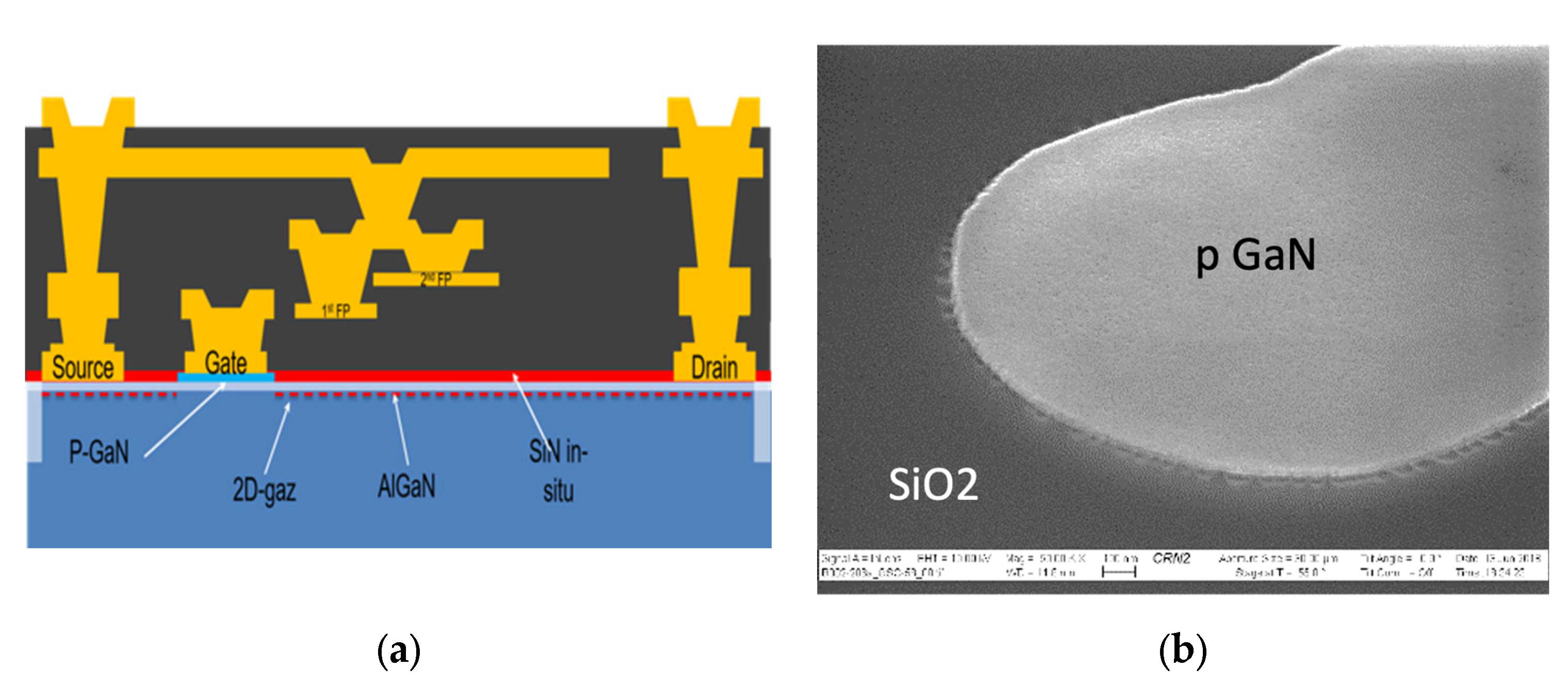
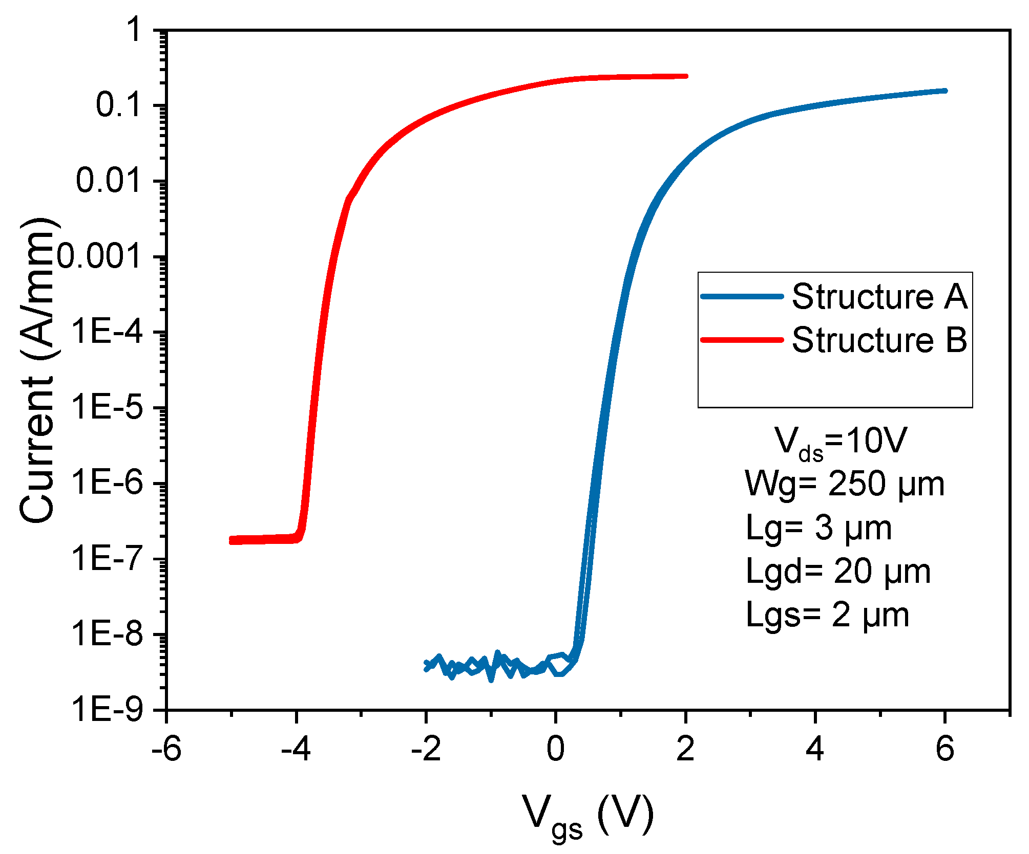
3. Devices Fabrication and Results
For the device fabrication, the structure B, was grown by EpiGaN on a Si (111) commercial wafer. The device fabrication and p-doped GaN layer regrowth were performed in the 3IT facility. For the p-doped GaN layer regrowth process, the wafer is protected by a 100 nm thick PECVD silicon oxide layer (SiO2) that acts as a mask for the regrowth. Following the patterning of this SiO2 layer, 100 nm of p-doped GaN was selectively grown using a CBE reactor. The growth temperature was 900°C and the targeted Mg atomic doping was 4E19 cm
−3. With an expected activation ratio of 1% [
10], the targeted hole concentration was 4E17 cm
−3. In
Figure 6b, we can observe that the growth is happening only on the open area, with no observable growth on the SiO2 mask. After removing such mask using the wet etching, the device fabrication could be initiated with the Ti/Al/Ni/Au ohmic contact deposition step, using E-beam evaporation followed by a rapid thermal annealing. Then, device isolation is performed by N
+ ion multiple implantations. Afterwards, the gate electrode was fabricated using (Ti/Au /Ni) metallization deposited by E-beam evaporation. Finally, three passivation and metallization process have been performed to fabricate the two field plates and the final interconnection layer: first passivation (100 nm of SiO2), first field plate (Ti/Au, 20 nm/600 nm), second passivation (200 nm of SiO2), second field plate (Ti/Au, 20 nm/600 nm), third passivation (600 nm of SiO2) and final interconnexion metallization (Ti/Au, 40 nm/800 nm) (
Figure 6a).
The two types of devices have been fabricated on the same wafer: the first is Normally-OFF (Structure A) and the second is Normally-ON where the gate electrode is deposited directly on the AlGaN barrier layer.
The transfer plots of these two devices are presented in
Figure 7. We can observe that the presence of the regrown p-doped GaN layer is shifting the V
th from −3 to +1.5 V. The gate contact of the Normally-ON device is simple Schottky type, which explain the relatively high off-state leakage current of this device, compared to the Normally-OFF one.
In
Figure 8 are presented the I
ds(V
ds) and I
ds(V
gs) plots. The two plots are showing a negligeable level of hysteresis. Thanks to the p-doped GaN layer, the PN junction located between the gate electrode and the channel is reversely biased and then reduces the gate leakage current.
The Coss capacitance of the device A is presented in in
Figure 9a for V
ds up to 400 V. In this plot, we can observe the presence of two steps: one at 75 V and the other at around 200 V. These two steps are indicative of the two field plates of the device.
Four terminal breakdown measurements have been performed on the fabricated device (
Figure 9b). Indeed, at V
gs = 0 V, the V
ds was swept up to 600 V. We can observe that for V
ds below 400 V, the drain and the source current are quite similar. After 400 V, the substrate current starts to increase and, consequently, the drain current increases faster than the source current. This increase in the drain current will lead to the breakdown of the device. In these measurements, we observed that the difference between the drain and the source currents is equivalent to the substrate current. Furthermore, on the same device, the source and gate probes were lifted up to perform two terminal measurements by probing only the drain and the backside of the substrate. After measuring the I(V) characteristics, we observed that the substrate current vs. the drain voltage is similar to that presented in
Figure 9b. So, we can conclude that the breakdown of the device is due to substrate current and will happen underneath the drain electrode.