
Characterization of m-GaN and a-GaN Crystallographic Planes after Being Chemically Etched in TMAH Solution

 , , ,
, , ,
Abstract
:1. Introduction
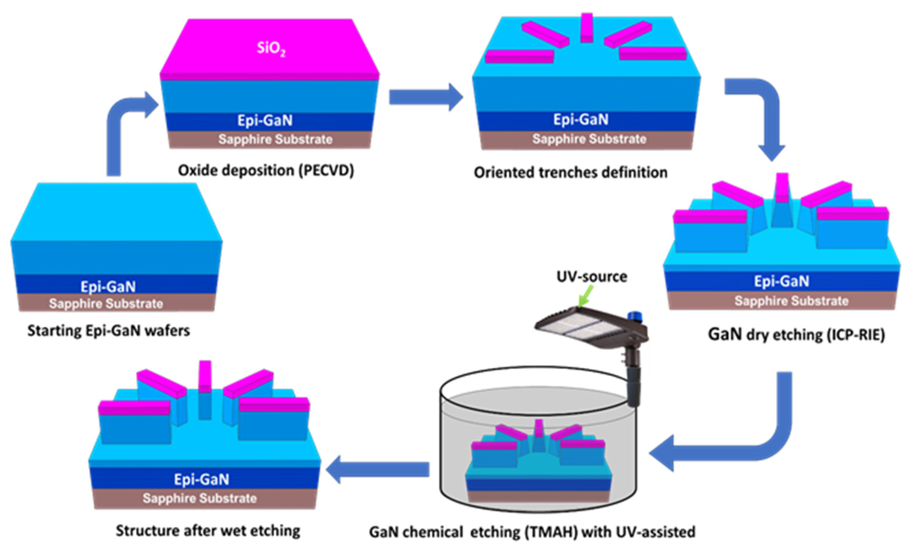
2. Experiment Technique
3. Results and Discussion
3.1. GaN Channel Sidewalls Etching Using the Proposed OD Procedure
3.2. Investigation of the Morphology of the Groove Surrounding the Fins after TMAH Etching
3.3. GaN Non-Polar Planes Wet Etching Rate Estimation in TMAH Solution with and without UV Source Utilization
4. Conclusions
Author Contributions
Funding
Data Availability Statement
Acknowledgments
Conflicts of Interest
References
- Li, R.; Cao, Y.; Chen, M.; Chu, R. 600 V/1.7—Normally-off GaN vertical trench metal–oxide–semiconductor field-effect transistor. IEEE Electron Device Lett. 2016, 37, 1466–1469. [Google Scholar] [CrossRef]
- Conole, G.; Hall, M.; Smith, S. Enabling professional communication for practitioners across Europe. Int. Conf. Comput. Educ. Proc. 2003, 47, 659–660. [Google Scholar] [CrossRef]
- Baliga, B. Power semiconductor device figure of merit for high-frequency applications. IEEE Electron Device Lett. 1989, 10, 455–457. [Google Scholar] [CrossRef]
- Baliga, B.J. Gallium nitride devices for power electronic applications. Semicond. Sci. Technol. 2013, 28. [Google Scholar] [CrossRef]
- Ma, C.-T.; Gu, Z.-H. Review of GaN HEMT Applications in Power Converters over 500 W. Electronics 2019, 8, 1401. [Google Scholar] [CrossRef] [Green Version]
- Tsao, J.Y.; Chowdhury, S.; Hollis, M.A.; Jena, D.; Johnson, N.M.; Jones, K.A.; Kaplar, R.J.; Rajan, S.; Van de Walle, C.G.; Bellotti, E.; et al. Ultrawide-Bandgap Semiconductors: Research Opportunities and Challenges. Adv. Electron. Mater. 2018, 4. [Google Scholar] [CrossRef] [Green Version]
- Amano, H.; Baines, Y.; Beam, E.; Borga, M.; Bouchet, T.; Chalker, P.R.; Charles, M.; Chen, K.J.; Chowdhury, N.; Chu, R.; et al. The 2018 GaN power electronics roadmap—IOP science. J. Phys. D Appl. Phys. Top. 2018, 51, 3001. [Google Scholar]
- Chowdhury, S.; Mishra, U.K. Lateral and Vertical Transistors Using the AlGaN/GaN Heterostructure. IEEE Trans. Electron Devices 2013, 60, 3060–3066. [Google Scholar] [CrossRef]
- Chakroun, A.; Jaouad, A.; Soltani, A.; Arenas, O.; Aimez, V.; Ares, R.; Maher, H. AlGaN/GaN MOS-HEMT Device Fabricated Using a High Quality PECVD Passivation Process. IEEE Electron Device Lett. 2017, 38, 779–782. [Google Scholar] [CrossRef]
- Cheney, D.J.; Douglas, E.A.; Liu, L.; Lo, C.-F.; Gila, B.P.; Ren, F.; Pearton, S.J. Degradation Mechanisms for GaN and GaAs High Speed Transistors. Materials 2012, 5, 2498–2520. [Google Scholar] [CrossRef]
- Ben-Yaacov, I.; Seck, Y.-K.; Mishra, U.K.; Denbaars, S. AlGaN/GaN current aperture vertical electron transistors with regrown channels. J. Appl. Phys. 2004, 95, 2073–2078. [Google Scholar] [CrossRef] [Green Version]
- Huang, H.; Li, F.; Sun, Z.; Sun, N.; Zhang, F.; Cao, Y.; Zhang, H.; Tao, P. Gallium Nitride Normally-Off Vertical Field-Effect Transistor Featuring an Additional Back Current Blocking Layer Structure. Electronics 2019, 8, 241. [Google Scholar] [CrossRef] [Green Version]
- Xiao, M.; Gao, X.; Palacios, T.; Zhang, Y. Leakage and breakdown mechanisms of GaN vertical power FinFETs. Appl. Phys. Lett. 2019, 114, 163503. [Google Scholar] [CrossRef]
- Zubair, A.; Perozek, J.; Niroula, J.; Aktas, O.; Odnoblyudov, V.; Palacios, T. First Demonstration of GaN Vertical Power FinFETs on Engineered Substrate. In Proceedings of the 2020 Device Research Conference (DRC), Columbus, OH, USA, 21–24 June 2020; pp. 1–2. [Google Scholar]
- Li, W.; Chowdhury, S. Design and fabrication of a 1.2 kV GaN-based MOS vertical transistor for single chip normally off operation. Phys. Status Solidi Appl. Mater. Sci. 2016, 213, 2714–2720. [Google Scholar] [CrossRef]
- Abdul Khadar, R.M.; Liu, C.; Soleimanzadeh, R.; Matioli, E. Fully Vertical GaN-on-Si power MOSFETs. IEEE Electron Device Lett. 2019, 40, 443–446. [Google Scholar] [CrossRef]
- Shibata, D.; Kajitani, R.; Ogawa, M.; Tanaka, K.; Tamura, S.; Hatsuda, T. 1.7 kV/1.0—Normally-off Vertical GaN Transistor on GaN substrate with Regrown p-GaN/AlGaN/GaN Semipolar Gate Structure. In Proceedings of the 2016 IEEE International Electron Devices Meeting (IEDM), San Francisco, CA, USA, 3–7 December 2016; pp. 248–251. [Google Scholar]
- Xiao, M.; Palacios, T.; Zhang, Y. ON-Resistance in Vertical Power FinFETs. IEEE Trans. Electron Devices 2019, 66, 3903–3909. [Google Scholar] [CrossRef]
- Sokolovskij, R.; Sun, J.; Santagata, F.; Iervolino, E.; Li, S.; Zhang, G.; Sarro, P. Precision Recess of AlGaN/GaN with Controllable Etching Rate Using ICP-RIE Oxidation and Wet Etching. Procedia Eng. 2016, 168, 1094–1097. [Google Scholar] [CrossRef]
- Shah, A.P.; Azizur Rahman, A.; Bhattacharya, A. Temperature-dependence of Cl2/Ar ICP-RIE of polar, semipolar, and non-polar GaN and AlN following BCl3/Ar breakthrough plasma. J. Vac. Sci. Technol. A 2020, 38, 013001. [Google Scholar] [CrossRef]
- Zhu, K. Evolution of surface roughness of AlN and GaN induced by inductively coupled Cl2/Ar plasma etching. J. Appl. Phys. 2004, 95, 4635–4641. [Google Scholar] [CrossRef] [Green Version]
- Merlos, A.; Acero, M.C.; Bao, M.; Bausells, J.; Esteve, J. TMAH/IPA anisotropic etching characteristics. Sens. Actuators A Phys. 1993, 37–38, 737–743. [Google Scholar] [CrossRef]
- Zhang, Y.; Sun, M.; Liu, Z.; Piedra, D.; Hu, J.; Gao, X.; Palacios, T. Trench formation and corner rounding in vertical GaN power devices. Appl. Phys. Lett. 2017, 110, 193506. [Google Scholar] [CrossRef]
- Wei, T.; Duan, R.; Wang, J.; Li, J.; Huo, Z.; Yang, J.; Zeng, Y. Microstructure and optical properties of non-polar m-plane GaN films grown on m-plane sapphire by hydride vapor phase epitaxy. Jpn. J. Appl. Phys. 2008, 47, 3346–3349. [Google Scholar] [CrossRef]
- Dannecker, K.; Baringhaus, J. Fabrication of crystal plane oriented trenches in gallium nitride using SF6 + Ar dry etching and wet etching post-treatment. J. Vac. Sci. Technol. A 2020, 38, 043204. [Google Scholar] [CrossRef]
- Tsai, M.C.; Leung, B.; Balakrishnan, G.; Wang, G.T. Understanding and Predicting GaN Anisotropic Wet Etch Facet Evolution Practical Motivation Etch rates of c-plane GaN for various chemistries. In Proceedings of the Electronic Material Conference, Zhengzhou, China, 11–12 April 2016; pp. 1–26. [Google Scholar]
- Pearton, S.; Shul, R.J.; Ren, F. A Review of Dry Etching of GaN and Related Materials. MRS Internet J. Nitride Semicond. Res. 2000, 5, 1–38. [Google Scholar] [CrossRef] [Green Version]
- Tautz, M.; Díaz, D.D. Wet-Chemical Etching of GaN: Underlying Mechanism of a Key Step in Blue and White LED Production. ChemistrySelect 2018, 3, 1480–1494. [Google Scholar] [CrossRef]
- Zhang, Y.; Sun, M.; Wong, H.Y.; Lin, Y.; Srivastava, P.; Hatem, C.; Azize, M.; Piedra, D.; Yu, L.; Sumitomo, T.; et al. Origin and Control of OFF-State Leakage Current in GaN-on-Si Vertical Diodes. IEEE Trans. Electron Devices 2015, 62, 2155–2161. [Google Scholar] [CrossRef] [Green Version]
- Fatahilah, M.F.; Strempel, K.; Yu, F.; Vodapally, S.; Waag, A.; Wasisto, H.S. 3D GaN nanoarchitecture for field-effect transistors. Micro Nano Eng. 2019, 3, 59–81. [Google Scholar] [CrossRef]
- Hwang, J.; Ho, K.; Hwang, Z.; Hung, W.; Lau, K.M.; Hwang, H.-L. Efficient wet etching of GaN and p-GaN assisted with chopped UV source. Superlattices Microstruct. 2004, 35, 45–57. [Google Scholar] [CrossRef]
- Powell, R.J.; Derbenwick, G.F. Vacuum ultraviolet radiation effects in SiO 2(Vacuum UV irradiation of silicon dioxide, discussing positive charging for photon energies above threshold for electron-hole pair creation). IEEE Trans. Nucl. Sci. 1971, 18, 99–105. [Google Scholar] [CrossRef]
- Jun-Lin, L.; Jian-Li, Z.; Guang-Xu, W.; Chun-Lan, M.; Long-Quan, X.; Jie, D.; Quan, Z.-J.; Wang, X.-L.; Pan, S.; Zheng, C.-D. Status of GaN-based green light-emitting diodes. Chin. Phys. B 2015, 24, 7804–7810. [Google Scholar]
- Kim, K.W.; Jung, S.D.; Kim, D.S.; Kang, H.S.; Im, K.S.; Oh, J.J.; Ha, J.-B.; Shin, J.-K.; Lee, J.H. Effects of TMAH treatment on device performance of normally off Al2O3/GaN MOSFET. IEEE Electron Device Lett. 2011, 32, 1376–1378. [Google Scholar] [CrossRef]
- Leung, B.; Tsai, M.C.; Li, C.; Liu, S.; Figiel, J.J.; Allerman, A.A.; Crawford, M.; Balakrishnan, G.; Brueck, S.; Wang, G.T. Crystallographic Etching of GaN: Fundamentals and Applications to Nanostructure Synthesis; Sandia National Lab. (SNL-NM): Albuquerque, NM, USA, 2011. [Google Scholar]
- Sun, Y.; Kang, X.; Zheng, Y.; Wei, K.; Li, P.; Wang, W.; Liu, X.; Zhang, G. Optimization of Mesa Etch for a Quasi-Vertical GaN Schottky Barrier Diode (SBD) by Inductively Coupled Plasma (ICP) and Device Characteristics. Nanomaterials 2020, 10, 657. [Google Scholar] [CrossRef] [PubMed] [Green Version]
- Lee, S.; Mishkat-Ul-Masabih, S.; Leonard, J.T.; Feezell, D.F.; Cohen, D.A.; Speck, J.S.; Nakamura, S.; DenBaars, S.P. Smooth and selective photo-electrochemical etching of heavily doped GaN:Si using a mode-locked 355 nm mi-crochip laser. Appl. Phys. Express 2017, 10, 10–13. [Google Scholar] [CrossRef]
- Stocker, D.A.; Schubert, E.F.; Redwing, J.M. Crystallographic wet chemical etching of GaN. Appl. Phys. Lett. 1998, 73, 2654–2656. [Google Scholar] [CrossRef] [Green Version]
- Zhuang, D.; Edgar, J. Wet etching of GaN, AlN, and SiC: A review. Mater. Sci. Eng. R Rep. 2005, 48, 1–46. [Google Scholar] [CrossRef]
- Chen, W.; Lin, J.; Hu, G.; Han, X.; Liu, M.; Yang, Y.; Wu, Z.; Liu, Y.; Zhang, B. GaN nanowire fabricated by selective wet-etching of GaN micro truncated-pyramid. J. Cryst. Growth 2015, 426, 168–172. [Google Scholar] [CrossRef]
- Horikiri, F.; Fukuhara, N.; Ohta, H.; Asai, N.; Narita, Y.; Yoshida, T.; Mishima, T.; Toguchi, M.; Miwa, K.; Sato, T. Simple wet-etching technology for GaN using an electrodeless photo-assisted electrochemical reaction with a luminous array film as the UV source. Appl. Phys. Express 2019, 12, 031003. [Google Scholar] [CrossRef] [Green Version]


| Ref | Authors | Wafer/Substrate | GaN Wet Etching Recipe | UV Light | Etch Time (min) | Mask | β | |
|---|---|---|---|---|---|---|---|---|
| m-GaN (nm/min) | a-GaN (nm/min) | |||||||
| 1 | This work | GaN/GaN | TMAH, 25%, 85 °C | Yes | 14 | Ti/Au/Ni | 1.09 | 4.69 |
| 2 | This work | GaN/GaN | TMAH, 25%, 85 °C | No | 14 | Ti/Au/Ni | 0.69 | 2.95 |
| 3 | B. Leung et al. [35] | GaN/GaN | TMAH, 25%, 80 °C | No | 52 | SiO2 | 0.13 | 0.16 |
| 4 | F. Horikiri et al. [41] | GaN/GaN | TMAH, 25%, 85 °C | Yes | 30 | SiO2 | 0.1-2 | --- |
Publisher’s Note: MDPI stays neutral with regard to jurisdictional claims in published maps and institutional affiliations. |
© 2021 by the authors. Licensee MDPI, Basel, Switzerland. This article is an open access article distributed under the terms and conditions of the Creative Commons Attribution (CC BY) license (https://creativecommons.org/licenses/by/4.0/).
Share and Cite
Al Taradeh, N.; Frayssinet, E.; Rodriguez, C.; Morancho, F.; Sonneville, C.; Phung, L.-V.; Soltani, A.; Tendille, F.; Cordier, Y.; Maher, H. Characterization of m-GaN and a-GaN Crystallographic Planes after Being Chemically Etched in TMAH Solution. Energies 2021, 14, 4241. https://doi.org/10.3390/en14144241
Al Taradeh N, Frayssinet E, Rodriguez C, Morancho F, Sonneville C, Phung L-V, Soltani A, Tendille F, Cordier Y, Maher H. Characterization of m-GaN and a-GaN Crystallographic Planes after Being Chemically Etched in TMAH Solution. Energies. 2021; 14(14):4241. https://doi.org/10.3390/en14144241
Chicago/Turabian StyleAl Taradeh, Nedal, Eric Frayssinet, Christophe Rodriguez, Frederic Morancho, Camille Sonneville, Luong-Viet Phung, Ali Soltani, Florian Tendille, Yvon Cordier, and Hassan Maher. 2021. "Characterization of m-GaN and a-GaN Crystallographic Planes after Being Chemically Etched in TMAH Solution" Energies 14, no. 14: 4241. https://doi.org/10.3390/en14144241
APA StyleAl Taradeh, N., Frayssinet, E., Rodriguez, C., Morancho, F., Sonneville, C., Phung, L.-V., Soltani, A., Tendille, F., Cordier, Y., & Maher, H. (2021). Characterization of m-GaN and a-GaN Crystallographic Planes after Being Chemically Etched in TMAH Solution. Energies, 14(14), 4241. https://doi.org/10.3390/en14144241