Article

Influence of Thermal Phenomena on the Characteristics of Selected Electronics Networks

Department of Marine Electronics, Faculty of Electrical Engineering, Gdynia Maritime University, Morska 83, 81-225 Gdynia, Poland
*
Author to whom correspondence should be addressed.
Energies 2021, 14(16), 4750; https://doi.org/10.3390/en14164750
Submission received: 15 June 2021 / Revised: 29 July 2021 / Accepted: 2 August 2021 / Published: 4 August 2021
(This article belongs to the Collection Feature Papers in Thermal Management)

Abstract

:
This paper presents the results of investigations on the influence of thermal phenomena—self-heating in semiconductor devices and mutual thermal couplings between them—on the characteristics of selected electronics networks containing bipolar transistors (BJTs) or insulated gate bipolar transistors (IGBTs). Using the authors’ compact electrothermal models of the transistors mentioned above, the non-isothermal DC and dynamic characteristics of these devices and selected networks with these devices are calculated. Their selected characteristics are compared with the measurement results. The waveforms of currents in the considered networks are also determined taking into account thermal phenomena. Discrepancies between the obtained calculation and measurement results and the calculation results obtained without thermal phenomena are indicated. In particular, attention is paid to cooling conditions at which the networks under consideration may be damaged due to thermal phenomena.

Graphical Abstract

1. Introduction

Electronic networks include semiconductor devices of different types [1,2,3], for example: diodes and bipolar or unipolar transistors. During the operation of these devices, the electrical energy dissipated in them is converted into heat, causing an increase in their internal temperature Tj as a result of thermal phenomena such as self-heating and mutual thermal couplings [2,4,5]. In this article temperature Tj denotes the temperature of a semiconductor die, which is an active part of semiconductor devices. An increase in temperature Tj changes the values of the coordinates of the operating points of these devices [4].
As shown i.a. in [6,7], the self-heating phenomenon causes changes in the course of the characteristics of semiconductor devices. These changes are both quantitative and qualitative [8,9,10]. The characteristics determined taking into account thermal phenomena are called non-isothermal characteristics, in contrast to the isothermal characteristics determined for a fixed value of the internal temperature.
In order to compute non-isothermal characteristics of semiconductor devices, an electrothermal analysis should be performed. In the literature many papers, e.g., [11,12,13,14,15,16,17] consider different aspects of electrothermal analyses. The papers [11,12] describe such an analysis performed with the use of compact electrothermal models, which use only one internal device temperature to characterize thermal properties of semiconductor devices. On the other hand, in [13] a hierarchical method of the electrothermal analysis is proposed. The reference [14] a semi-analytic method for the electrothermal analysis of a thin-film resistor is proposed. Reference [15] describes a method of the dynamic electrothermal analysis of electronic circuits. The electrothermal analysis can be used for analyses of big power modules [16] and small, nanoscale transistors [17].
Specialized software is commonly used for the analysis and design of electronic circuits, e.g., the SPICE software [18,19]. The accuracy of the calculations carried out with this software depends on the accuracy of the models of the used components of the analyzed network. The models embedded in the SPICE software are isothermal models [20], but the literature contains many papers on electrothermal models of electronic components dedicated to this software [7,21,22,23,24,25,26]. These models typically take into account additional component (positive or negative) of voltage or current due to thermal phenomena by means of controlled voltage or current sources. In turn, the value of the internal temperature is represented in such models by voltage on an additional network, which is an electrical analog of the thermal model of the considered device [4,27,28,29].
The papers [6,10,22] show that non-isothermal characteristics of semiconductor devices may have a significantly different shape from the isothermal characteristics. In particular, non-isothermal characteristics of these devices may not be functions in the mathematical sense, i.e., one independent variable value corresponds to several dependent variable values. Quite frequently on such current-voltage characteristics there is an electrothermal breakdown point, where the sign of the slope of such a characteristic changes from positive to negative [21,22]. Additionally, in the case of the transient analysis, significant changes in the operating point of transistors contained in electronic circuits caused by thermal phenomena may be visible [30].
For electronic circuits containing more than one semiconductor device, mutual thermal couplings between these devices may occur, causing an additional increase in the internal temperature of each of these devices due to power dissipation in other semiconductor devices placed on a common printed circuit board [31], on a common heat sink [32] or in a common case [33]. These couplings are characterized by mutual transient thermal impedances, and the waveforms of these impedances depend on the method of assembly of the considered devices [34], e.g., on the area of soldering pads, the distance between semiconductor devices, the dimensions of the used heat-sink or properties of the used thermal interfaces.
This paper presents some results of measurements and computations illustrating an influence of thermal phenomena on properties of selected transistors and electronics networks containing these transistors. Computations are performed using the authors’ compact electrothermal models dedicated to the SPICE software. An influence of cooling conditions on non-isothermal DC characteristics of power BJTs, IGBTs and power modules is shown and discussed. Attention is paid on the antypical (different than visible in the catalogue data) shape of these characteristics and possibility of destroying such devices operating inside the safe operating area. Using the same models the non-isothermal DC and dynamic characteristics of selected electronics networks are computed. Investigations were carried out for the following networks: transistor switch, differential amplifier and parallel connection of two transistors. An influence of self-heating in the transistors and mutual thermal couplings between them on these characteristics is considered and discussed. Many examples illustrating a risk of damage of semiconductor devices operating in these networks are shown and discussed. It is also shown that in selected cases mutual thermal couplings can protect the analyzed networks against damage. On the other hand, it is shown that the operating point of the analyzed networks can dramatically change after a long time of operation of the considered networks. Some suggestions how to protect these networks and how use thermal couplings to stabilize the operating points of these networks are formulated.

2. Compact Electrothermal Models of Semiconductor Devices

The first compact electrothermal models of semiconductor devices were described in the literature as early as the beginning of the 1970s [35]. These models took the form of a system of equations describing:
(a)
the relationship between currents and voltages of the modeled device, in which the internal temperature of this device is present;
(b)
the dependence of the power dissipated in a semiconductor device on their terminal voltages and currents;
(c)
the dependence of the device internal temperature on the power dissipated in it.
The first attempts to use the SPICE software to model non-isothermal characteristics of semiconductor devices were described in the literature at the turn of the 1980s and 1990s [36,37]. These models use an electrical and thermal analogy in which the relevant electronics network represents the thermal model of the device. In this network, the voltages in the nodes represent the temperature of individual components of the heat flow path, and the currents flowing in particular branches—the power released in the semiconductor device.
The general form of an electrothermal compact model of a semiconductor device for the SPICE software is shown in Figure 1. The considered electrothermal model consists of three components: the electrical model of the form given by the function f(v,i) describing the relationship between voltages v and currents i of the modeled device, the power model of the form given by the function g(v,i) enabling the determination of the power pth dissipated in the modeled device and the thermal model described by the function h(pth), in which the value of the internal temperature Tj is calculated, appearing in the equations representing an electrical model. The electrical model has a different form for each semiconductor device and is typically formulated as an electronics network containing an electrical analog of the equations describing the characteristics of the device being modeled. Such models have been described in many articles, e.g., [23] for diodes, [7,21] for BJTs, [21,38] for IGBTs, [26] for power MOSFETs, [39] for operational amplifiers and [40] for integrated circuits used in switching mode power supplies.
The classic version of the compact thermal model uses linear resistors (with fixed values of resistance) and capacitors (fixed values of capacitance) representing thermal resistances and thermal capacitances of the thermal model, respectively [27,41,42,43]. It was shown in [44] that the thermal resistance of a bipolar transistor depends on the operating point of this device. Reference [45] proposes compact nonlinear thermal models of semiconductor devices taking into account the influence of ambient temperature, internal temperature and power dissipated on the cooling efficiency of these devices. In turn [46] proposes an analytical description of the dependence of thermal resistance of an electronic component on the design of the cooling system of these devices. It was experimentally shown that by optimizing the cooling system it is possible to reduce the value of thermal resistance up to 50 times.
In the paper [22], a non-linear thermal model of the IGBT was used to formulate its electrothermal model. It was experimentally shown that such a model allows for better modeling accuracy than the electrothermal model using the linear thermal model.
The compact thermal model of networks containing more semiconductor devices makes it possible to determine the internal temperature of each of these devices taking into account self-heating and mutual thermal couplings between each pair of these devices. Reference [28] proposes a form of such a model using the concept of a matrix of transient thermal impedances. In the paper [33] the method of implementing such a model in SPICE was presented. In the case of a thermal coupling between two semiconductor devices, the internal temperature of the first device Tj1 can be described by:
T j 1 t = T a + 0 t Z t h 1 t v p 1 v d v + 0 t Z t h 12 t v p 2 v d v
where Ta is the ambient temperature, p1(t)—power dissipated in this device, Zth1(t)—time derivative of the transient thermal impedance of this device, p2(t)—power dissipated in the second device thermally coupled with the device under consideration, Zth12(t)—time derivative of the mutual thermal transient impedance between the devices under consideration, whereas v is an integration variable. Both the mentioned transient thermal impedances are typically approximated by the relationship of the following form [27,41]:
Z t h t = R t h 1 i = 1 N a i exp t τ t h i
where Rth is thermal resistance, ai—the coefficients associated with particular thermal time constants τthi, and N—the number of these time constants.
The detailed descriptions of the compact electrothermal models of BJTs are described in [21], and of IGBTs—in [22].

3. Non-Isothermal Characteristics of Selected Transistors

Using the compact electrothermal BJTs and IGBTs models described in the papers [9,10], the non-isothermal DC characteristics of selected types of these transistors were determined. The obtained calculation results were compared with the measurement results in Figure 2, Figure 3 and Figure 4.
Values of currents and voltages corresponding to the points lying in non-isothermal characteristics were measured with the use of APPA 207 digital multimeters using the classical indirect method. The results of measurements were registered when the thermally steady state was obtained. All the measurements were performed only ones. Therefore, only type B evaluation of uncertainty is used. According to information given by the manufacturer [47], the relative uncertainty of the measured values is smaller than ±0.2% for currents and ±0.06% for voltages. In turn, isothermal characteristics were measured using the pulse method and a Keithley 2612A source-meter. The relative uncertainty of these measurements did not exceed ±0.06% for currents and ±0.02% for voltages [48]. In order to compute the value of standard uncertainty the values of given above values of relative uncertainty should be multiplied by the value of the used measurement range. The maximum values of the measurement uncertainty are given at description of each figure presented in this Section. In each of these figures error bars are shown. Due to very small values of standard uncertainty typically the error bars are invisible (they are smaller than squares representing measurement results).
Figure 2 illustrates the output characteristics of the selected power BJT of the type 2N3055 [49] at selected values of base current iB and the fixed value of the ambient temperature Ta = 34 °C. In this figure, points denote the results of measurements, solid lines—the results of electrothermal analyses, and dashed lines—the results of isothermal analyses. The standard uncertainty of measured voltage does not exceed ±0.24 V, whereas this uncertainty for measured current does not exceed ±20 mA. Due to so small values of standard uncertainty the error bars are invisible (they are smaller than the squares representing measurement results). Electrothermal analyses were performed using the electrothermal models of the devices included in the considered networks, whereas isothermal analyses were performed using the isothermal models of such devices.
As can be seen, the results of the electrothermal analyses match the measurement results very well (the differences between them do not exceed 3.5%), while the isothermal characteristics differ in shape from the measured characteristics. The isothermal characteristics show a positive slope and are visible in the breakdown range at voltage vCE exceeding 70 V. On the other hand, the electrothermal breakdown point is visible on the non-isothermal characteristics.
As seen, the non-isothermal characteristics have the qualitatively different shape, depending on the value of the base current. These characteristics have a positive slope in the active mode (before the electrothermal breakdown point Ai) at the base current equal to 1 mA and 10 mA. This slope is negative at higher values of the base current (iB = 100 mA and 300 mA) This means that the local minimum near the electrothermal breakdown point always occurs on these characteristics. The internal temperature of the BJT in the points Ai is higher than 200 °C. This means that they are outside the safe operating area of the transistor.
It should be noted that power BJTs could have S-type and N-type non-isothermal output characteristics. The N-type characteristics are seen at high base currents, outside the device safe operation area. This N-type shape results from the influence of the collector current and temperature on the coefficient of current amplification.
In turn, Figure 3 shows the output characteristics of the IGBT of the IRG4PC40UD type [50] determined for selected values of the gate-emitter voltage vGE and different cooling conditions. These characteristics are shown in Figure 3a for the transistor operating without any heat-sink and in Figure 3b for the transistor situated on the heat-sink. During the measurements the heat-sink was situated horizontally on the wooden table. The transistor was screwed to the top part of this heat-sink and the silicon paste was used as a thermal interface.
In this figure, points denote the results of measurements, solid lines—the results of electrothermal analyses performed with the use of the model from the paper [22], and dashed lines—the results of analyses performed with the use of the Hefner model [20,51]. For the considered values of voltage VGE the results obtained using the Hefner model overlap with the VCE-axis. The standard uncertainty of measured voltage does not exceed ±24 mV, whereas this uncertainty for measured current does not exceed ±8 mA.
At both the types of the cooling conditions the ambiguous characteristics IC(VCE) are obtained. The point of the electrothermal breakdown, in which the sign of the slope of these characteristics changes from positive to negative, is visible on each characteristic. Such a shape of the considered characteristics also means that the breakdown in the investigated transistor can appear at a value of voltage VCE which is considerably lower than the admissible catalog value.
As it is visible in Figure 3 the breakdown can appear even for VCE smaller than 10 V, whereas the admissible value of this voltage given by the producer amounts to 600 V [50]. It is worth observing that VCE value, at which the electrothermal breakdown appears, decreases with an increase in VGE voltage and a worsening of its cooling conditions.
As shown in [22], the point of the electrothermal breakdown corresponds to the case where the temperature TC is equal to about 50 °C. The value of this temperature is practically the same for both the considered cooling conditions [22]. Similar qualitatively characteristics were also obtained for power MOS transistors. These characteristics are shown and discussed in [52].
In the examples shown in Figure 2 and Figure 3a change in the course of the output characteristics of the considered transistors is caused only by the self-heating phenomenon. In order to illustrate the influence of thermal couplings on the characteristics of the transistors placed in the common case, Figure 4 shows the output characteristics of the IGBT included in the PSI25/06 type power module manufactured by Power Sem [53]. This module contains two IGBT transistors marked as T1 or T2 and two diodes.
In Figure 4 the output characteristics of transistor T1 contained in the examined module obtained at the gate-emitter voltage VGE1 = 6.6 V are shown. In Figure 4a the isothermal characteristics obtained at different values of ambient temperature are shown. In this case power is dissipated in transistor T1 only. The standard uncertainty of measured voltage does not exceed ±20 mV, whereas this uncertainty for measured current does not exceed ±0.6 mA. Figure 4b shows the results of the investigations performed with thermal phenomena taken into account at the ambient temperature equal to 25 °C. In these investigations power of different values is dissipated in the other components of the module (power pD2 in diode D2 and power pT2 in transistor T2). In this figure the horizontal black dashed line marks the isothermal characteristic of the investigated transistor. The standard uncertainty of measured voltage does not exceed ±24 mV, whereas this uncertainty for measured current does not exceed ±8 mA.
As it is visible, the shape of the non-isothermal characteristics shown in Figure 4b visibly differs from the isothermal characteristics presented in Figure 4a. The non-isothermal characteristics are not any functions in a mathematical sense. One can see on them the point of the electrothermal breakdown. The value of voltage VCE1, at which appears the point of the electrothermal breakdown, decreases together with an increase of the power dissipated in the other components of the module. The value of the collector current of the investigated transistor increases as a result of thermal phenomena at an increase in the power dissipated in the other components of this module. It is also proper to notice that dissipation of power of the same value in transistor T2 causes a stronger influence on the course of the characteristic IC1(VCE1) of transistor T1 than the dissipation of this power in diode D2. It is also shown in [54] that changes of the shape of the characteristics IC1(VCE1) are accompanied by essential changes in temperature of the module. As a result of mutual thermal couplings between the components of the considered module a temperature rise of the components of this module is equal to even 100 °C.

4. Non-Isothermal Characteristics of Electronics Networks

Using the compact electrothermal models of the BJTs and IGBTs described in [9,10], the DC and dynamic characteristics of selected electronic systems containing these semiconductor devices are determined. The results of these calculations are shown in Section 4.1, Section 4.2, Section 4.3. Some of the calculation results are compared with the measurement results. The tests were carried out for the transistor switch (Section 4.1), paralelly connected transistors (Section 4.2) and a differential amplifier (Section 4.3). In all the figures presenting the investigation results, lines indicate the results of calculations and points—the results of measurements.

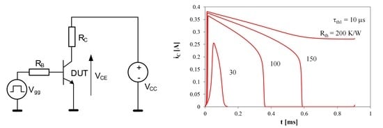
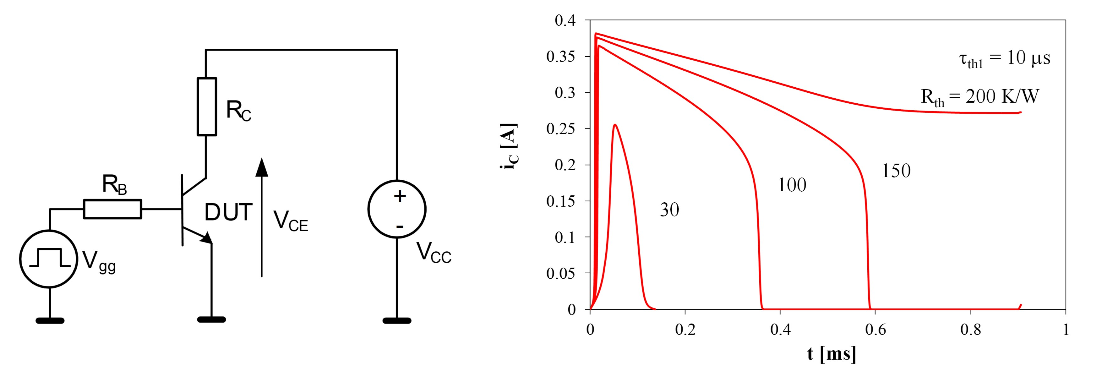
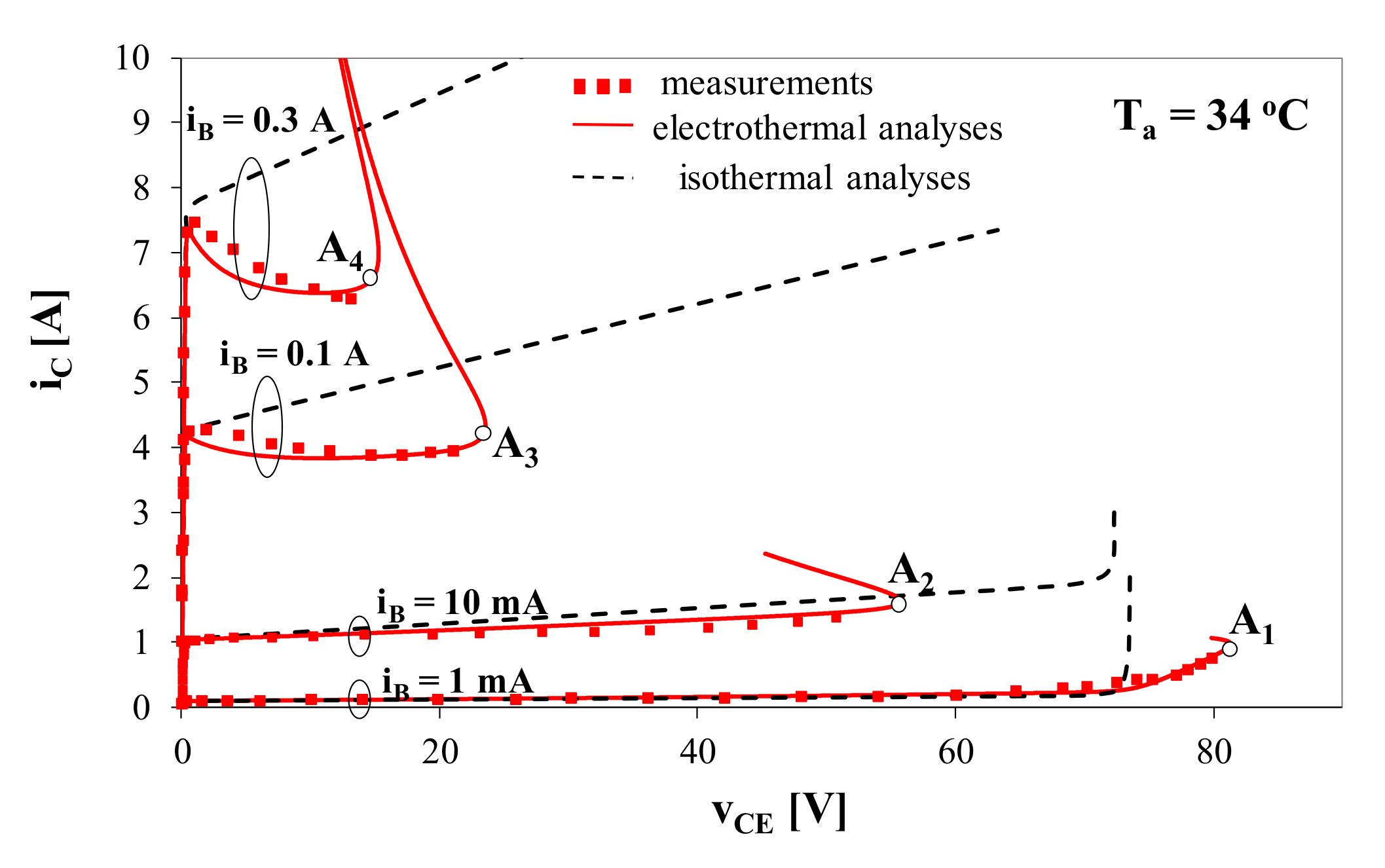
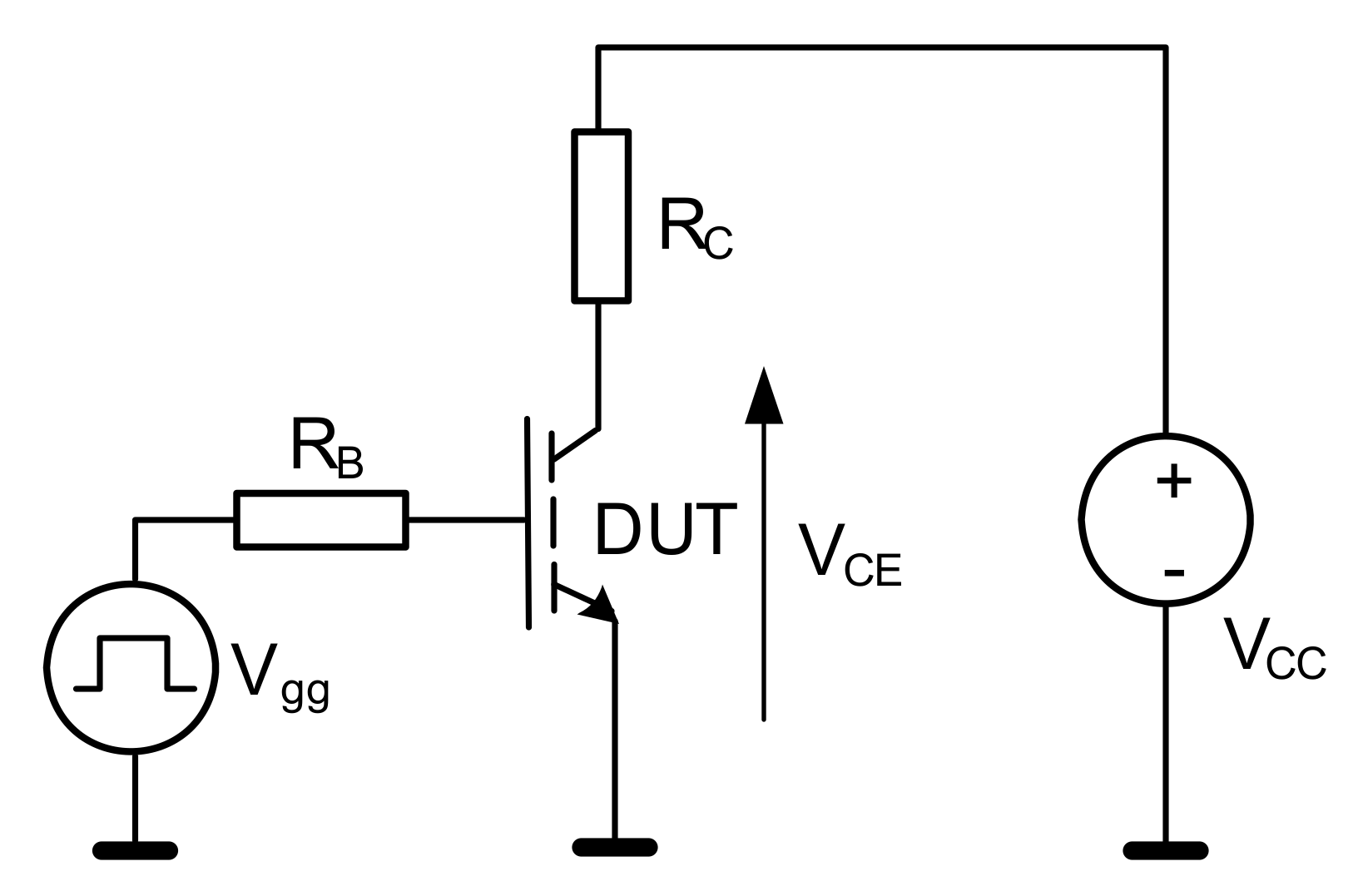
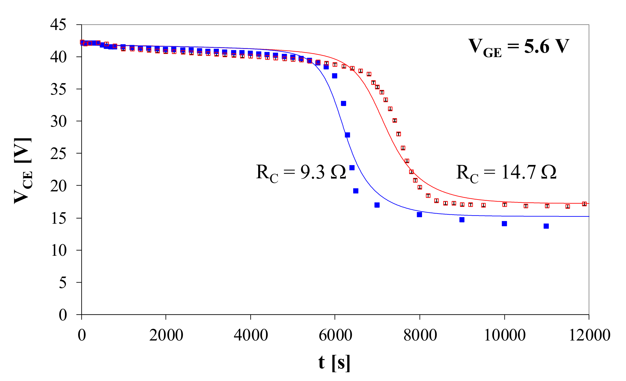
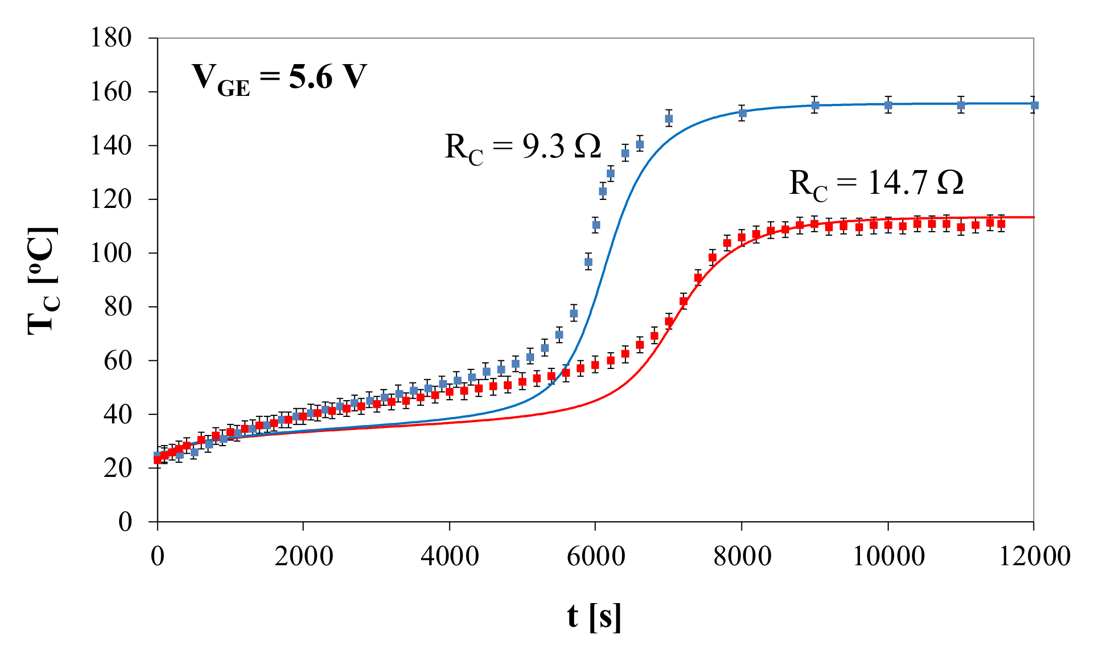
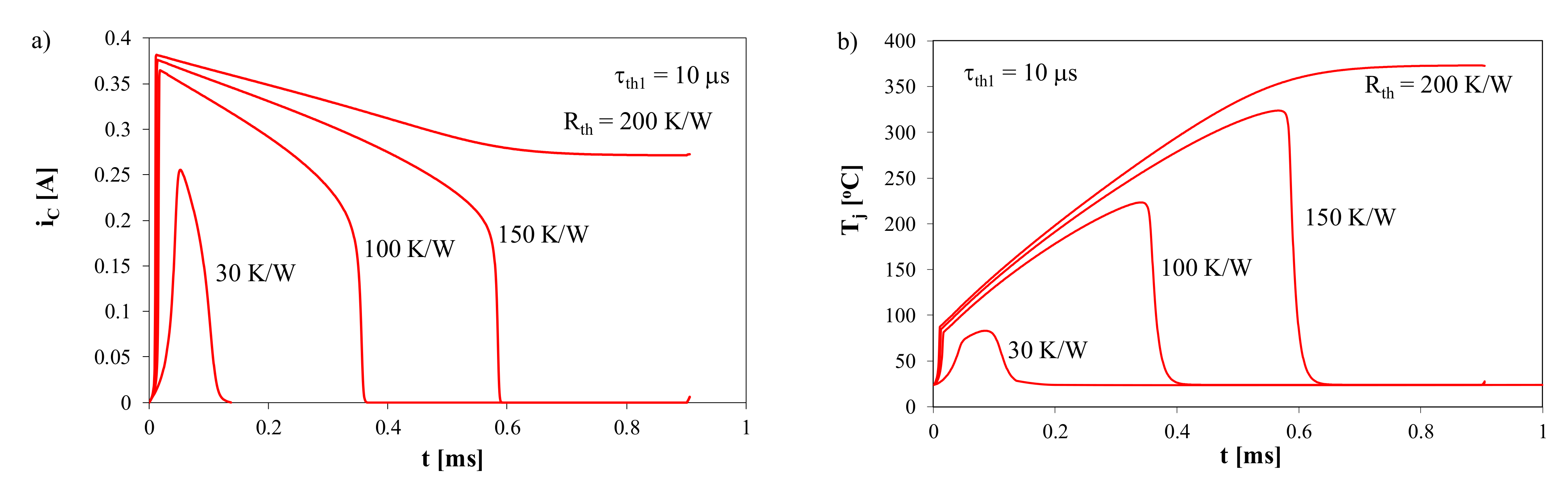
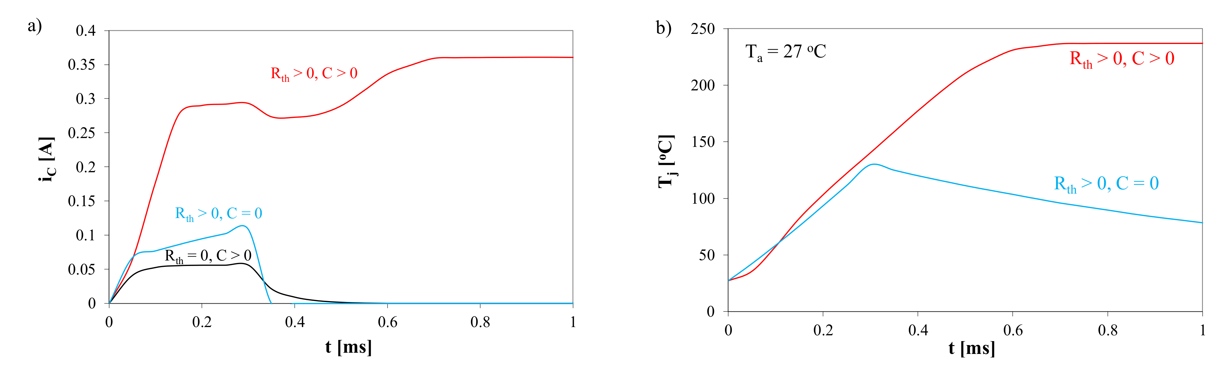
4.1. Transistor Switch

This Section presents the results of testing a transistor switch circuit containing a BJT or IGBT transistor. Figure 5 shows the considered network including the IGBT. In this circuit, a DC voltage source VCC polarizing the collector of the transistor and a voltage source Vgg are used. The source Vgg generates voltage of the shape of a rectangular pulses train exciting the transistor’s gate. The measurements of currents and voltage waveforms were performed with the use of APPA207 multimeters connected with a PC registering the results of the measurements. The case temperature of the tested transistors were measured using an Optex PT-3S infrared pyrometer [55] with the analog voltage output connected to an APPA207 multimeter. The dedicated software made it possible to register values of the measured currents and voltage with the constant time step of the minimum value equal to 0.5 s. Information about uncertainty of voltages and currents measurements performed with the APPA207 are given at the beginning of Section 3. In turn, according to information given by the manufacturer standard uncertainty of temperature measurements using considered pyrometer does not exceed ±3 °C [55].
Figure 6 shows the calculated and measured waveforms of voltage VCE obtained when the voltage on the source Vgg has the shape of a voltage step of the value equal to 5.6 V and voltage VCC = 43 V. The resistor RC has in the following experiments the resistance of the values equal to 9.3 Ω or 14.7 Ω. Such properties of operation of the considered network are selected in order to obtain the operating point of the IGBT near the point of the electrothermal breakdown. The waveforms of the device case temperature corresponding to the presented waveforms of VCE voltage are shown in Figure 7. The measurements, the results of which are shown in Figure 6 and Figure 7, were performed with the time step equal to 0.5 s. The standard uncertainty of measured voltage does not exceed ±240 mV, whereas this uncertainty for measured case temperature does not exceed ±3 °C.
It is worth observing that the steady state on the waveform of voltage VCE appears only after 2 h after switching-on the voltage on the transistor gate. At that time the temperature of the case TC of the investigated transistor increases from 23 °C to 110 °C (Figure 7). This temperature rise causes a decrease in the voltage of the transistor threshold voltage and consequently, an increase in the value of the collector current. Finally, it leads to a fall of voltage VCE. When resistance RC = 9.3 Ω the transistor goes to the on-state 6000 s after switching on the power supply and its case temperature at the steady state exceeds 150 °C. For a higher value of the resistance RC the time indispensable to obtain the steady state increases and attains even 7500 s. This increase is a result of a decrease in a slope of the load line and a decrease in the value of power dissipated in the IGBT. In comparison, if VCC voltage is much higher than the electrothermal breakdown voltage, the steady state can be obtained for this transistor already after about 10 min after switching-on the power supply.
Similar investigations were carried out for the switch containing a BJT. In this case, the following values of the components of the circuit from Figure 5 were adopted: VCC = 13.5 V, RC = 112 Ω, RB = 0 Ω, a high value of voltage Vgg equals to 0.63 V. The obtained results of computations and measurements are shown in Figure 8. The standard uncertainty of measured current does not exceed ±80 μA. The time resolution of iC measurements is equal to 1 s.
As seen from Figure 8a, the collector current IC and the junction temperature change rapidly their values after about 6500 s from the moment of switching on the power supply. This collector current rise is caused by thermal inertia of the BJT and its thermally steady state is reached after the mentioned time. The BJT has the DC non-isothermal output characteristic with vBE = 0.63 V at the ambient temperature Ta = 30 °C shown in Figure 8b with the load line (blue solid line). As seen, when the thermally steady state at the point of the electrothermal breakdown (point A) is not attained, the operation point moves to B in the low collector-emitter voltage region to reach the thermally steady state and this situation is called the electrothermal breakdown. In Figure 8b dashed lines correspond to the non-isothermal dc characteristics at the ambient temperature equal to Ta1 = 25 °C and Ta2 = 35 °C. As seen, a rise in the ambient temperature can cause the above-described effect as well. It is worth mentioning that the junction temperature at the point A is equal to about 50 °C. Whether this switching effect results in the functional or catastrophic failure depends, for example on the coordinates of the point B, but above all on the junction temperature at this point. In the considered case the junction temperature Tj is equal to 84 °C at the thermally steady state (Figure 8a). Due to the discrepancy between the measured and computed output characteristics of the BJT in the range of high values of IC current (Figure 8b), the measured and computed values of this current after switching it on (Figure 8a) differ between each other even by 10%.
The previously presented examples illustrate the problem of delayed switching on of the transistor switch due to thermal phenomena. In the next part of this Section the problem of an influence of thermal phenomena and electrical inertia of the BJT on the switching off process of such a switch is considered. The following values of the parameters of the network from Figure 5 were adopted in the simulation tests: VCC = 20 V, RC = 50 Ω, RB = 10 kΩ, while the voltage source Vgg generates a single pulse with the duration of tD = 30 μs and the value of 5 V. In order to simplify the analyses it was assumed that in the thermal model of the transistor there is only one thermal time constant τth = 10 μs. The analyses were performed for various values of thermal resistance Rth.
As shown in Figure 9a, if the value of Rth is less than 150 K/W, then the BJT is off. Higher values of Rth demand the longer time to reach off-state (far longer than the duration time of the input pulse). At higher values of Rth the device can fail before being off, due to its junction temperature rise. At Rth = 200 K/W, the BJT is in the thermally steady state and the value of its junction temperature is far beyond the admissible value (Figure 9b). As the computations showed, two things cause this situation. Firstly, the forward biasing of the emitter junction by current of the reverse-biased collector junction can take place. This reverse current depends strongly on temperature, and it can cause the emitter-base voltage drop being sufficient for operation of the BJT in the forward active mode if the value of resistor RB is high enough. Secondly, the parasitic electrical capacitances C of the transistor junctions have to be discharged after the input pulse is off, and the voltage drop across them maintains the conducting of currents.
In Figure 10 the influence of the electrical capacitances in the model of the BJT is illustrated.
As seen Figure 10a, only the electrothermal model including elements modeling electrical inertia (C > 0) shows a possibility of functional failure, which in the considered circuit stands for a transistor being on, and in this case a high temperature rise can be observed (Figure 10b). This means that electrical capacitances make it possible to extend the time, at which the device internal temperature increases to such a high value that the reverse current of the base-collector junction is high enough to polarize base-emitter junction in the forward mode.

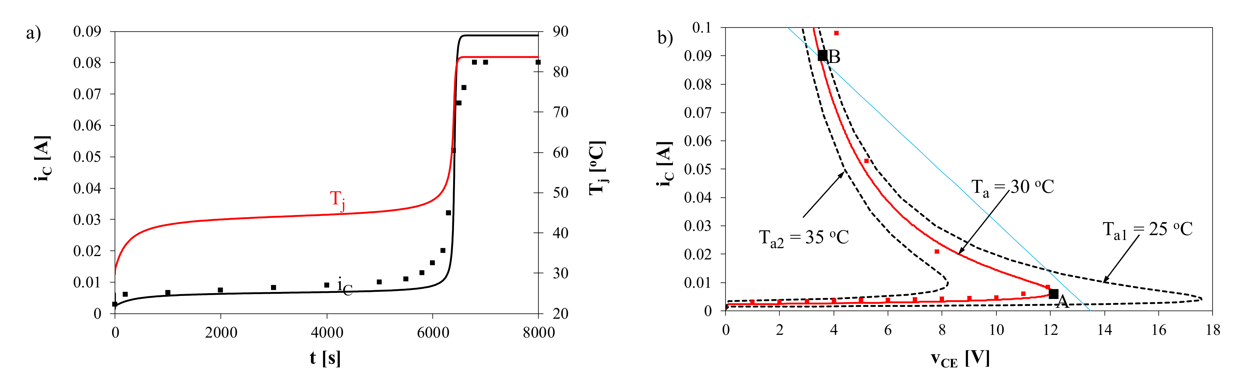
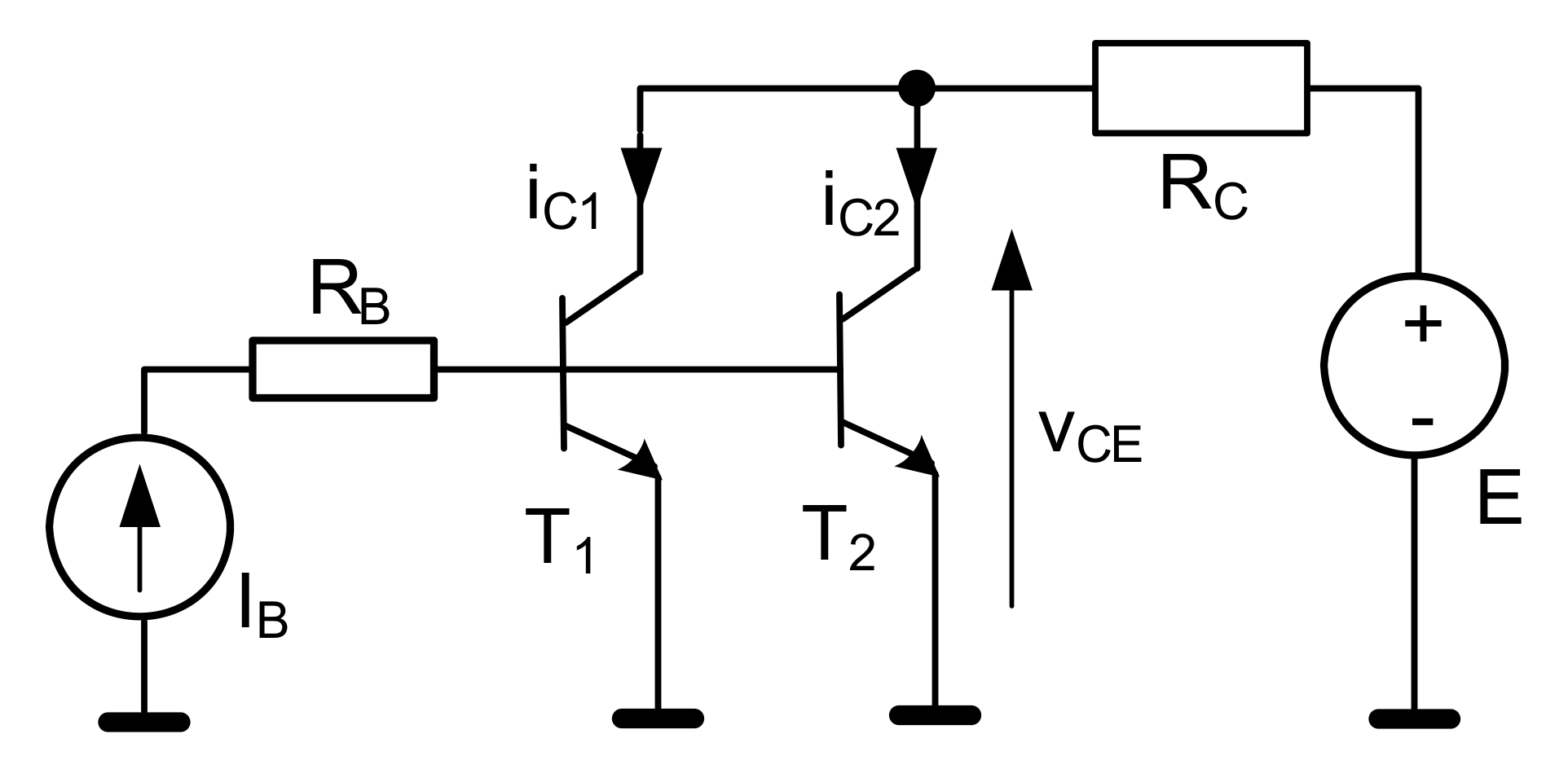
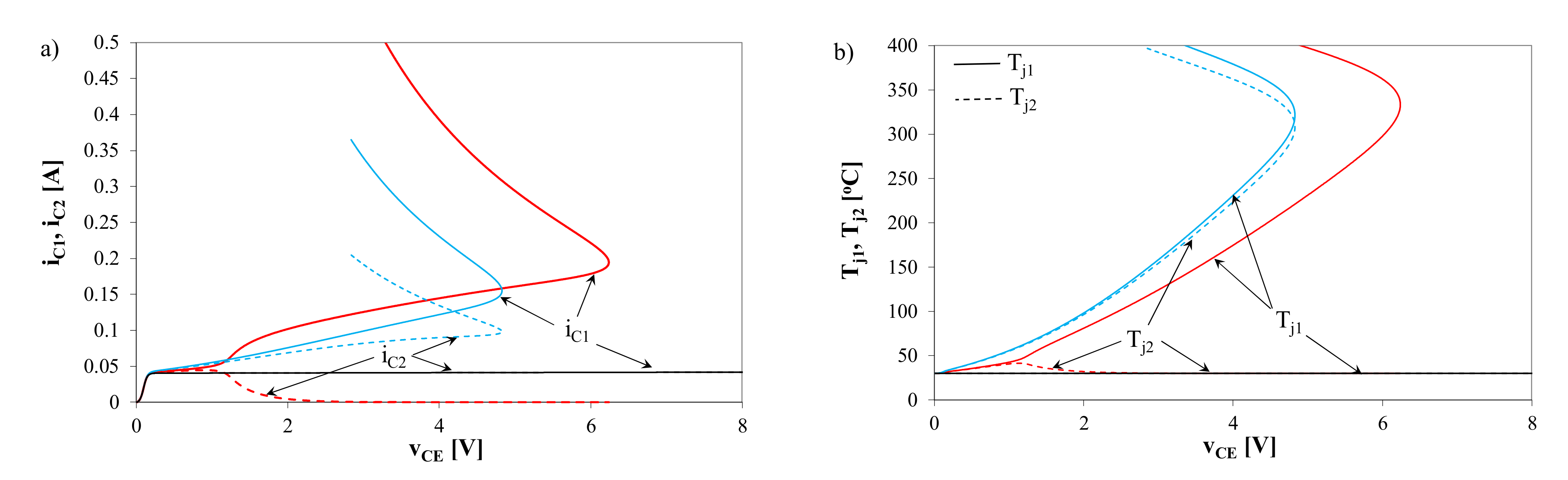
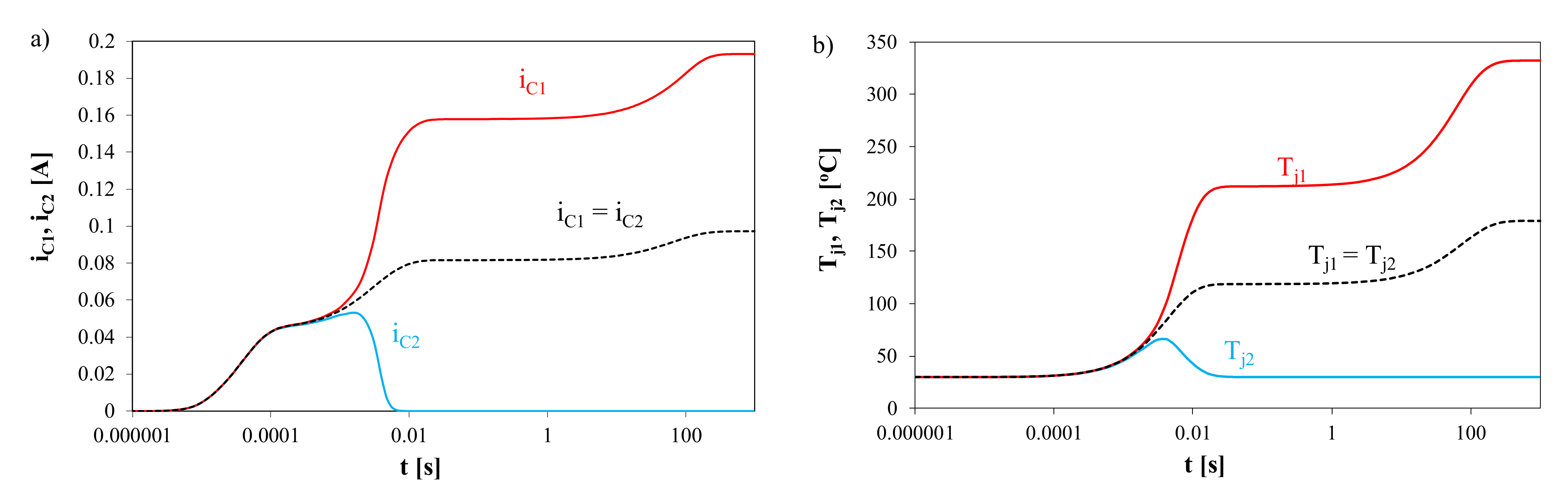
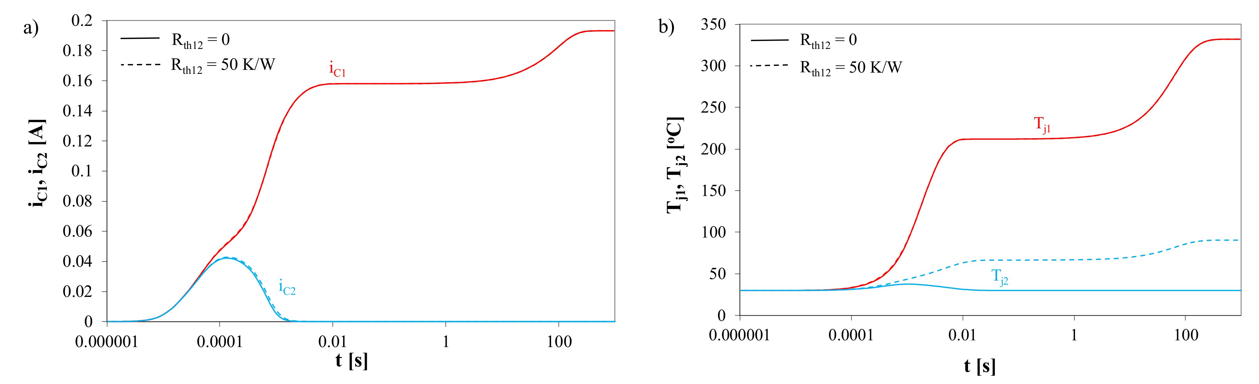
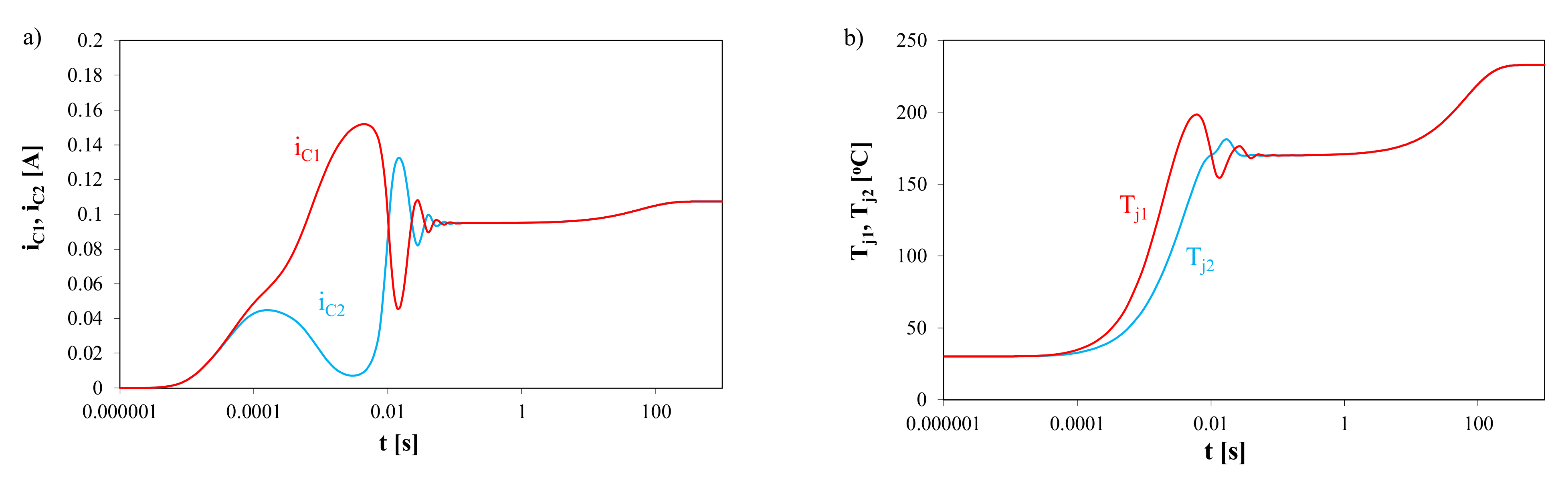
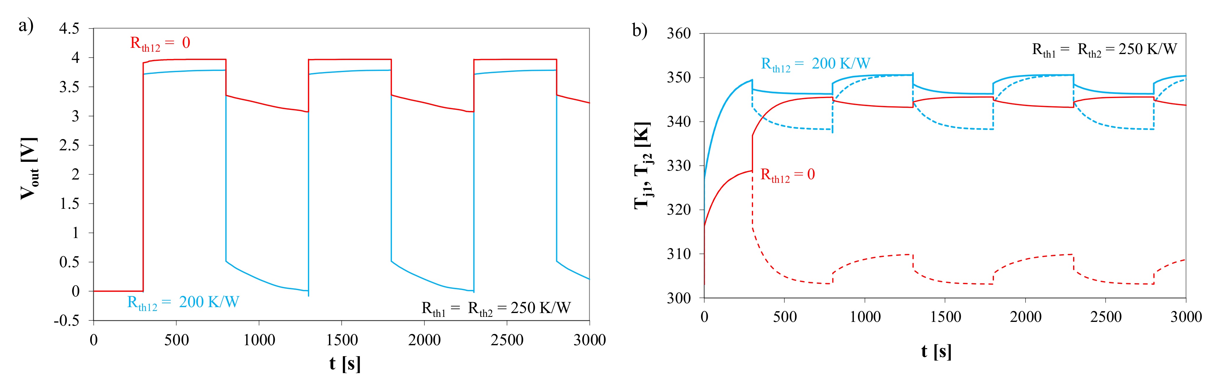
4.2. Two Parallelly Connected BJTs

The parallel connection of transistors is used in many power systems, where high current efficiency is required. In this Section, the problem of the influence of thermal phenomena on the operation of such a system containing BJTs is considered. The diagram of the analyzed system is shown in Figure 11. In this network voltage of the source E is equal to 25 V, resistor RC = 100 Ω and resistor RB = 5 kΩ.
Figure 12 shows the non-isothermal DC characteristics of the system under consideration determined for a fixed current value IB = 0.25 mA. It was assumed that both the transistors have identical values of all electrical parameters, but slightly differ in the values of thermal parameters. Three cases were considered:
(a)
both the transistors are perfectly cooled and thermal resistance of each is zero (black lines),
(b)
the transistors are not thermally coupled, and their self thermal resistances are Rth1 = 250 K/W for transistor T1 and Rth2 = 240 K/W for transistor T2 (red lines),
(c)
the transistors are thermally coupled, their self thermal resistances are Rth1 = 250 K/W and Rth2 = 240 K/W, respectively, and the transfer thermal resistance between them is Rth12 = 220 K/W (blue lines).
As it is visible, under ideal cooling conditions the collector currents of both the transistors are the same, and the dependences of these currents on voltage VCE are monotonically increasing functions. On the other hand, with imperfect cooling and the absence of mutual thermal couplings, it can be seen that as voltage VCE increases, the difference between the collector currents of both the transistors (iC1 and iC2) increases. Transistor T1 with a higher value of thermal resistance conducts more and more collector current as voltage VCE increases, and the other transistor—less and less collector current. Due to self-heating, transistor T1 enters the electrothermal breakdown range at voltage VCE = 6 V, at which current iC2 is close to zero. When taking into account the mutual thermal couplings between the transistors, the difference between the collector currents of these transistors is visible, but it does not exceed 80%. In this case also the shape of the iC(VCE) relationship for both the transistors is similar.
Figure 13, Figure 14, Figure 15 and Figure 16 show the waveforms of the currents in the system under consideration at different values of the parameters characterizing the thermal model of the system under consideration. In all the considered cases, the current source IB is turned on at t = 0. In these figures the logarithmic time-scale is used.
If BJTs have the same values of their electrical and thermal parameters, then they conduct the same collector current (Figure 13a) and their junction temperatures (Figure 13b) are identical. It is illustrated in Figure 13 by black dashed lines. But if only the values of their thermal resistances are different, the thermal failure can occur. This situation is shown in Figure 13, where red and blue solid lines relate to the BJTs with different values of their thermal resistances (the difference amounts 4%). As seen, when the thermally steady state T2 is off, and the junction temperature of T1 is far beyond the admissible value in contrast to the previous case, where the junction temperatures of BJTs reached the acceptable value.
In the circuit from Figure 11, the thermal failure can be caused by different values of the thermal time constants only. It is shown in Figure 14, where the mentioned difference leads to the thermally steady state, in which T2 is off, as previously. In the computations the following values of thermal time constants were assumed: τth1 = 2 ms, τth2 = 100 s for T1 and τth1 = 5 ms, τth2 = 100 s for T2, respectively. The device (T1) with the lower value of the shortest thermal time constant conducts the whole current and it can fail due to its junction temperature rise (Figure 14b).
The mutual thermal interactions between transistors T1 and T2 can also essentially influence the distribution of the current between the BJTs (the results presented in Figure 13 and Figure 15 were obtained without these interactions). It is illustrated in Figure 14 and Figure 15. The results given in Figure 14 relate to a weak thermal interaction: the transfer thermal resistance Rth12 = 50 K/W (dashed lines), whereas in Figure 15 a strong thermal interaction: Rth12 = 240 K/W. At the lower value of Rth12, transistor T1 (the device with the lower value of τth1 = 2 ms) can fail due to its junction temperature rise. But if the thermal coupling is strong, Rth12 = 240 K/W, then at the thermally steady state both the transistors have the same values of their collector currents and the junction temperatures. Before steady state is reached, the oscillations of the mentioned quantities are seen (Figure 15).
The thermal couplings between the devices can be especially strong in integrated circuits or in a power BJT with a large dimension split in some subdevices to carry out the electrothermal analysis on the basis of the compact electrothermal model of the device. It is worth to observe that mutual thermal couplings make it possible to reduce a difference between values of collector currents of both the BJTs and the values of their internal temperature. Therefore, in this case, thermal couplings protect the BJTs against a damage.

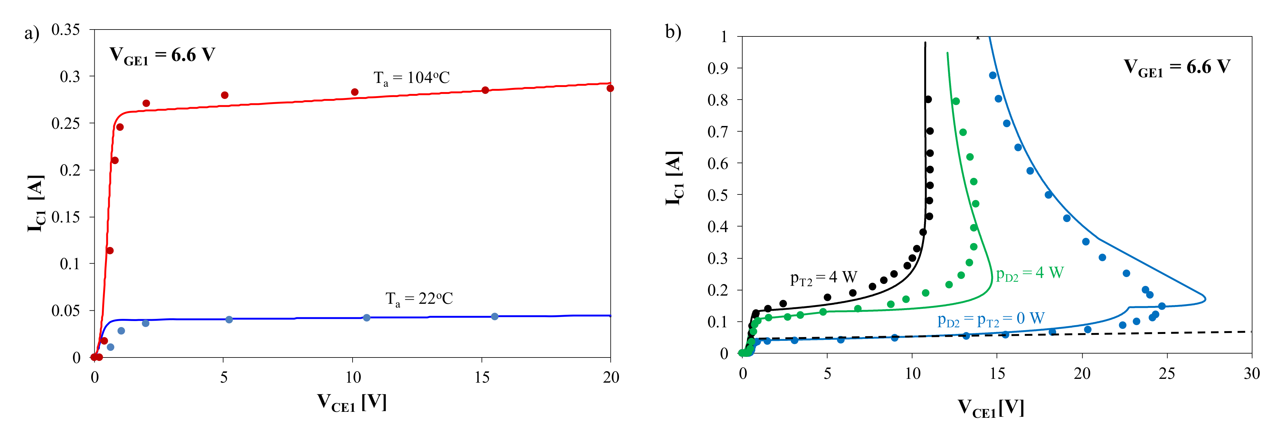
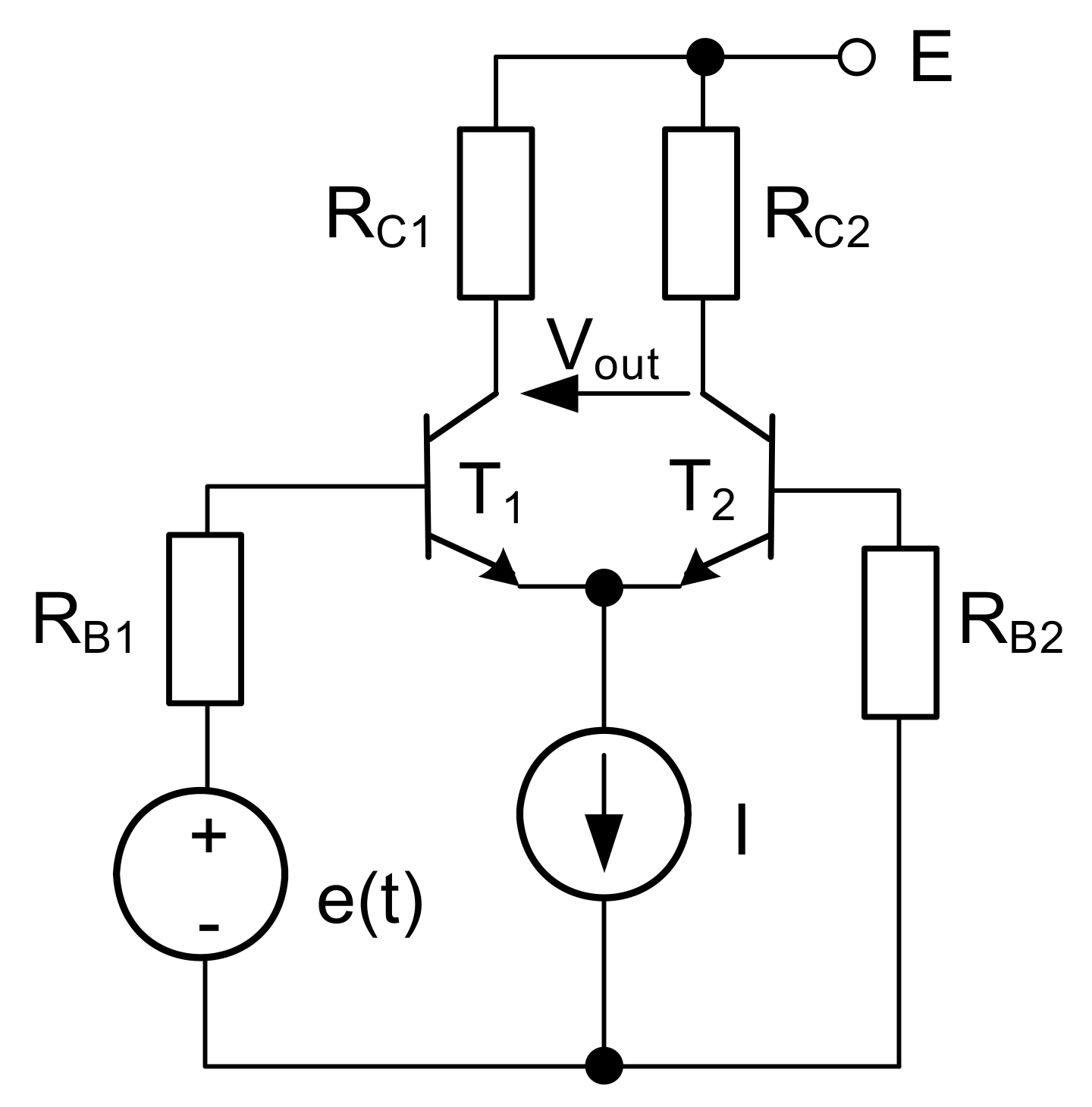
4.3. Differential Amplifier

In analog circuits, a differential amplifier circuit of the diagram shown in Figure 16 is often used. In this Section, the operation of this circuit is considered with the excitation voltage from the source e(t) of the shape of a rectangular pulses train. In this network the resistance of resistors RC1 and RC2 is equal to 200 Ω, the resistance of resistors RB1 and RB2 is equal to 1 kΩ, whereas the output current of the source I is equal to 20 mA. The supply voltage E is equal to 12 V.
Electrothermal analyses of the considered circuit were carried out for selected cooling conditions of both the transistors. Figure 17 and Figure 18 show the waveforms of the output voltage Vout (t) and the internal temperatures of the transistors included in the considered circuit Tj1(t) and Tj2(t). The calculations were made for the exciting voltage with the shape of a rectangular pulses train with the period of 1000 s, the duty cycle of 0.5 and the amplitude of 0.1 V.
Figure 17 shows the computation results obtained by ignoring the mutual thermal couplings between the transistors. The individual waveforms correspond to different values of thermal resistance of both the transistors in the range from 100 to 250 K/W. In Figure 17b, solid lines indicate the internal temperature of transistor T1, whereas dashed lines represent the internal temperature of transistor T2.
As can be observed in Figure 17a, after increasing of thermal resistance, the amplitude of the output voltage Vout decreases. This phenomenon results from the differences in the internal temperature values of transistors T1 and T2 visible in Figure 17b. The difference between these temperatures can even reach more than 40 °C. As it is known, the collector current of this transistor increases as the internal temperature of the BJT operating at a fixed value of the base current increases. Since the sum of the collector currents of both the transistors has a fixed value, an increase in the collector current of transistor T1 causes a decrease in the current of transistor T2. As a result, the considered circuit does not operate correctly and the shape of the output voltage differs significantly from the shape of the input voltage. It is worth noticing that this phenomenon occurs at a relatively low value of the temperature difference Tj1–Tj2.
Figure 18 shows the influence of mutual thermal couplings on the characteristics of the circuit under consideration. The computations were performed for a fixed value of thermal resistance of each of transistors Rth1= Rth2 = 250 K/W and selected values of mutual thermal resistance Rth12.
As can be seen, as the value of Rth12 increases, the shape of the voltage waveform Vout(t) changes more and more to correspond to the square wave pattern (Figure 18a). This is due to the mutual thermal couplings between the transistors causing the temperature difference Tj1–Tj2 to be much smaller than in the case shown in Figure 17b. Therefore, from the point of view of the proper operation of the considered system, it is important that the transfer thermal resistance has the values similar to self thermal resistance of each of the transistors. The easiest way to achieve this goal is to place the transistors in a common semiconductor die. It is also worth observing that in Figure 17 and Figure 18 the steady state is obtained for time t > 1300 s. At this steady state the waveforms of Vout(t), Tj1(t) and Tj2(t) are periodical functions.

5. Conclusions

The paper analyzes the influence of thermal phenomena on the DC and dynamic properties of selected semiconductor devices and electronic networks. It has been shown that the non-isothermal DC characteristics of BJTs and IGBTs may have a shape significantly different from that of the isothermal characteristics of these devices provided by their manufacturers and measured using the pulse method.
Some of the presented non-isothermal characteristics are not functions in the mathematical sense and may have an S-type or N-type shape. These characteristics show an electrothermal breakdown manifested by a change in the slope of the output characteristics of the transistors under consideration. The transistor output voltage, at which this phenomenon is visible, is typically much lower than the breakdown voltage declared by the manufacturer. In BJTs operating with the control of constant base current, the electrothermal breakdown occurs at the internal temperature exceeding the value permitted by the manufacturer (approx. 180–200 °C), while for IGBTs, this phenomenon is already observed at the internal temperature of approx. 60 °C.
In the case of the IGBTs included in a power module, it has been shown that the mutual thermal couplings between the components of this module significantly change the characteristics of the components of this module. The dissipation of power at a fixed value in another module component causes the internal temperature of the IGBT to rise and its output characteristics to be shifted to the left. It is worth noting that the influence of the power dissipation of the same value in two different components of the module causes a different increase of the internal temperature of the IGBT contained in this module and a different course of its characteristics.
The analysis of electronic circuits has shown that due to thermal phenomena, their DC and dynamic characteristics may significantly differ from the characteristics assumed by the designer of these circuits. In the transistor switch, a significant change in the operating point coordinates after switching can be observed if the supply voltage of the collector circuit slightly exceeds the value of the output voltage of the transistor corresponding to the electrothermal breakdown point. In this case, after 1–2 h from the moment of switching on the transistor, the value of its collector current may increase even several times. This phenomenon can damage the transistor contained in this circuit.
In a switch circuit with the BJT, with a high value of the resistor contained in the gate circuit and a high value of thermal resistance of this device, a significant increase in the transistor turn-off time can be observed, and even a latch-up effect can be obtained, at which the transistor cannot be turned off.
It has been shown in the BJT parallel connection circuit that in the absence of mutual thermal couplings between such transistors and even a slight difference between the values of their thermal resistance, after a short time almost all the current is taken over by the transistor with a higher value of thermal resistance. This disadvantageous phenomenon can be effectively counteracted by ensuring a strong thermal coupling between the transistors, e.g., by placing them on a common heat sink or in a common semiconductor die. When the transfer thermal resistance between the transistors is close to self thermal resistance of these transistors, the values of their collector currents differ slightly from each other.
In the case of a differential amplifier, the peak-to-peak value of the output voltage of this network is observed due to the self-heating phenomenon. The shape of the output voltage differs more from the shape of the input voltage, the higher the value of the thermal resistance of the transistors. Taking into account the mutual thermal couplings between the transistors included in this system allows concluding that the shape of the output voltage of the system is similar to the input voltage.
The results of the analyses presented in this paper prove that thermal phenomena can significantly affect the characteristics of the considered semiconductor devices and electronics networks. In particular, it has been shown that as a result of self-heating the operating point of the transistors in the circuits under consideration may change and, consequently, damage them. It has also been shown that for the correct operation of the considered circuits containing two transistors, mutual thermal couplings that allow minimizing the differences in temperature inside these transistors are important. These networks can only operate properly when such couplings are ensured. The presented investigation results and conclusions may be important for designers of analog and switching circuits.

Author Contributions

Conceptualization (K.G., J.Z. and P.G.); methodology (K.G. and J.Z.); investigation (K.G. and P.G.); writing—original draft preparation (K.G. and P.G); writing—review and editing (K.G., J.Z. and P.G); visualization (K.G. and P.G.); supervision (K.G.). All authors have read and agreed to the published version of the manuscript.

Funding

This research received no external funding.

Institutional Review Board Statement

Not applicable.

Informed Consent Statement

Not applicable.

Data Availability Statement

The presented experimental data can be made available on request.

Conflicts of Interest

The authors declare no conflict of interest.

References

  1. Rashid, M.H. Power Electronic Handbook; Butterworth-Heinemann: Oxford, UK, 2007. [Google Scholar]
  2. Perret, R. Power Electronics Semiconductor Devices; John Wiley & Sons: Hoboken, NJ, USA, 2009. [Google Scholar]
  3. Tietze, U.; Schenk, C.; Gamm, E. Electronic Circuits, Handbook for Design and Application; Springer: Heidelberg, Germany, 2008. [Google Scholar]
  4. Lasance, C.J.M.; Poppe, A. Thermal Management for LED Applications; Springer Science + Business Media: New York, NY, USA, 2014. [Google Scholar]
  5. Castellazzi, A.; Gerstenmaier, Y.C.; Kraus, R.; Wachutka, G.K.M. Reliability analysis and modeling of power MOSFETs in the 42-V-PowerNet. IEEE Trans. Power Electron. 2006, 21, 603–612. [Google Scholar] [CrossRef] [Green Version]
  6. D’alessandro, V.; Catalano, A.P.; Scognamillo, C.; Codecasa, L.; Zampardi, P.J. Analysis of electrothermal effects in devices and arrays in InGaP/GaAs HBT technology. Electronics 2021, 10, 757. [Google Scholar] [CrossRef]
  7. Mawby, P.A.; Igic, P.M.; Towers, M.S. Physically based compact device models for circuit modelling applications. Microelectron. J. 2001, 32, 433–447. [Google Scholar] [CrossRef]
  8. Sharmaand, D.K.; Ramanathan, K.V. Modeling Thermal Effects on MOS I-V Characteristics. IEEE Electron Devices Lett. 1983, 4, 362–364. [Google Scholar] [CrossRef]
  9. Wachutka, G.K. Rigorous thermodynamic treatment of heat generation and conduction in semiconductor device modeling. IEEE Trans. Comput. Aided Des. Integr. Circuits Syst. 1990, 9, 1141–1149. [Google Scholar] [CrossRef] [Green Version]
  10. Janke, W.; Hapka, A.; Oleksy, M. DC characteristics of the SiC Schottky diodes. Bull. Pol. Acad. Sci. Tech. Sci. 2011, 59, 183–188. [Google Scholar] [CrossRef] [Green Version]
  11. Choi, S.; Shim, S.; Shin, Y. Electrothermal Analysis with Nonconvective Boundary Conditions. IEEE Trans. Circuits Syst. II Express Briefs 2018, 65, 1044–1048. [Google Scholar] [CrossRef]
  12. Codecasa, L.; D’Amore, D.; Maffezzoni, P. Compact modeling of electrical devices for electrothermal analysis. IEEE Trans. Circuits Syst. I Fundam. Theory Appl. 2003, 50, 465–476. [Google Scholar] [CrossRef]
  13. Harris, T.R.; Priyadarshi, S.; Melamed, S.; Ortega, C.; Manohar, R.; Dooley, S.R.; Kriplani, N.M.; Davis, W.R.; Franzon, P.D.; Steer, M.B. Transient Electrothermal Analysis of Three-Dimensional Integrated Circuits. IEEE Trans. Compon. Packag. Manuf. Technol. 2012, 2, 660–667. [Google Scholar] [CrossRef]
  14. Vermeersch, B.; de Mey, G. Device level electrothermal analysis of integrated resistors. In Proceedings of the 14th International Conference on Mixed Design of Integrated Circuits and Systems: MIXDES 2007, Ciechocinek, Poland, 21–23 June 2007; pp. 375–380. [Google Scholar]
  15. Storti-Gajani, G.; Brambilla, A.; Premoli, A. Electrothermal dynamics of circuits: Analysis and simulations. IEEE Trans. Circuits Syst. I Fundam. Theory Appl. 2001, 48, 997–1005. [Google Scholar] [CrossRef]
  16. Li, X.; Li, D.H.; Qi, F.; Packwood, M.; Luo, H.Z.; Wang, Y.G.; Dai, X.P.; Luo, H.H.; Liu, G.Y. EM-Electrothermal Analysis of Semiconductor Power Modules. IEEE Trans. Compon. Packag. Manuf. Technol. 2019, 9, 1495–1503. [Google Scholar] [CrossRef]
  17. Cheng, A.Q.; Chen, S.T.; Zeng, H.; Ding, D.Z.; Chen, R.S. Transient Analysis for Electrothermal Properties in Nanoscale Transistors. IEEE Trans. Electron Devices 2018, 65, 3930–3935. [Google Scholar] [CrossRef]
  18. Rashid, M. SPICE for Power Electronics and Electronic Power, 3rd ed.; Taylor and Francis Group: Oxfordshire, UK, 2016. [Google Scholar]
  19. Basso, C. Switch-Mode Power Supply SPICE Cookbook; McGraw-Hill: New York, NY, USA, 2001. [Google Scholar]
  20. Wilamowski, B.; Jager, R.C. Computerized Circuit Analysis Using SPICE Programs; McGraw-Hill: New York, NY, USA, 1997. [Google Scholar]
  21. Zarębski, J.; Górecki, K. SPICE-aided modelling of dc characteristics of power bipolar transistors with selfheating taken into account. Int. J. Numer. Model. Electron. Netw. Devices Fields 2009, 22, 422–433. [Google Scholar] [CrossRef]
  22. Górecki, P.; Górecki, K.; Zarębski, J. Accurate circuit-level modelling of IGBTs with thermal phenomena taken into account. Energies 2021, 14, 2372. [Google Scholar] [CrossRef]
  23. Starzak, Ł.; Zubert, M.; Janicki, M.; Torzewicz, T.; Napieralska, M.; Jabłoński, G.; Napieralski, A. Behavioral approach to SiC MPS diode electrothermal model generation. IEEE Trans. Electron Devices 2013, 60, 630–638. [Google Scholar] [CrossRef]
  24. Marcault, E.; Massol, J.L.; Tounsi, P.; Dorkel, J.M. Distributed electrothermal modelling methodology for MOS gated power devices simulations. In Proceedings of the 20th International Conference on Mixed Design of Integrated Circuits and Systems, MIXDES 2013, Gdynia, Poland, 20–22 June 2013; pp. 301–305. [Google Scholar]
  25. Wu, R.; Wang, H.; Pedersen, K.B.; Ma, K.; Ghimire, P.; Iannuzzo, F.; Blaabjerg, F. A Temperature-Dependent Thermal Model of IGBT Modules Suitable for Circuit-Level Simulations. IEEE Trans. Ind. Appl. 2016, 52, 3306–3314. [Google Scholar] [CrossRef] [Green Version]
  26. Codecasa, L.; d’Alessandro, V.; Magnani, A.; Irace, A. Circuit-based electrothermal simulation of power devices by an ultrafast nonlinear MOS approach. IEEE Trans. Power Electron. 2016, 31, 5906–5916. [Google Scholar] [CrossRef]
  27. Bagnoli, P.E.; Casarosa, C.; Ciampi, M.; Dallago, E. Thermal resistance analysis by induced transient (TRAIT) method for power electronic devices thermal characterization. IEEE Trans. Power Electron. I Fundam. Theory 1998, 13, 1208–1219. [Google Scholar] [CrossRef]
  28. Schweitzer, D.; Ender, F.; Hantos, G.; Szabo, P.G. Thermal transient characterization of semiconductor devices with multiple heat-sources—Fundamentals for a new thermal standard. Microelectron. J. 2015, 46, 174–182. [Google Scholar] [CrossRef]
  29. D’Alessandro, V.; Rinaldi, N. A critical review of thermal models for electro-thermal simulation. Solid State Electron. 2002, 46, 487–496. [Google Scholar] [CrossRef]
  30. Górecki, K.; Górecki, P. Modelling dynamic characteristics of the IGBT with thermal phenomena taken into account. Microelectron. Int. 2017, 34, 160–164. [Google Scholar] [CrossRef]
  31. Shahjalal, M.; Ahmed, M.R.; Lu, H.; Bailey, C.; Forsyth, A.J. An Analysis of the Thermal Interaction Between Components in Power Converter Applications. IEEE Trans. Power Electron. 2020, 35, 9082–9094. [Google Scholar] [CrossRef]
  32. Górecki, K. Modelling mutual thermal interactions between power LEDs in SPICE. Microelectron. Reliab. 2015, 55, 389–395. [Google Scholar] [CrossRef]
  33. Górecki, P.; Górecki, K. Measurements and computations of internal temperatures of the IGBT and the diode situated in the common case. Electronics 2021, 10, 210. [Google Scholar] [CrossRef]
  34. Yuan, W.B.; He, Y.G.; Li, B.; Zhou, J.B.; Ma, Z.Q.; Li, C.C. Improved Cauer thermal network considering thermal coupling effects of multi-chip modules. IET Power Electron. 2020, 13, 3706–3716. [Google Scholar] [CrossRef]
  35. Nemeth, K. On the Analysis of Nonlinear Resistive Networks Considering the Effect of Temperature. IEEE J. Solid State Circuits 1976, 11, 550–552. [Google Scholar] [CrossRef]
  36. Vogelsong, R.S.; Brzezinski, C. Simulation of Thermal Effects in Electrical Systems. In Proceedings of the Fourth Annual IEEE Applied Power Electronics Conference and Exposition, Baltimore, MD, USA, 13–17 March 1989; pp. 353–356. [Google Scholar]
  37. Bielefeld, J.; Pelz, G.; Abel, H.B.; Zimmer, G. Dynamic SPICE-Simulation of the Electrothermal Behavior of SOI MOSFET’s. IEEE Trans. Electron Devices 1995, 42, 1968–1974. [Google Scholar] [CrossRef]
  38. Riccio, M.; de Falco, G.; Mirone, P.; Maresca, L.; Tedesco, M.; Breglio, G.; Irace, A. Accurate SPICE Modeling of Reverse-Conducting IGBTs Including Self-Heating Effects. IEEE Trans. Power Electron. 2017, 32, 3088–3098. [Google Scholar] [CrossRef]
  39. D’Alessandro, V.; Catalano, A.P.; Codecasa, L.; Moser, B.; Zampardi, P.J. Modeling Thermal Coupling in Bipolar Power Amplifiers toward Dynamic Electrothermal Simulation. In Proceedings of the 2018 IEEE MTT-S International Conference on Numerical Electromagnetic and Multiphysics Modeling and Optimization (NEMO), Reykjavik, Iceland, 8–10 August 2018; pp. 1–4. [Google Scholar] [CrossRef]
  40. Zarębski, J.; Górecki, K. SPICE-Aided Modelling of the UC3842 Current Mode PWM Controller with Selfheating Taken into Account. Microelectron. Reliab. 2007, 47, 1145–1152. [Google Scholar] [CrossRef]
  41. Szekely, V. A New Evaluation Method of Thermal Transient Measurement Results. Microelectron. J. 1997, 28, 277–292. [Google Scholar] [CrossRef]
  42. Infineon, Transient Thermal Measurements and Thermal Equivalent Circuit Models, AN 2015-10, v. 1.2. 2020. Available online: https://www.infineon.com/dgdl/Infineon-Thermal_equivalent_circuit_models-ApplicationNotes-v01_02-EN.pdf?fileId=db3a30431a5c32f2011aa65358394dd2 (accessed on 29 January 2021).
  43. Sofia, J.W. Analysis of thermal transient data with synthesized dynamic-models for semiconductor-devices. IEEE Trans. Compon. Packag. Manuf. Technol. Part A 1995, 18, 39–47. [Google Scholar] [CrossRef]
  44. Oettinger, F.F.; Blackburn, D.L.; Rubin, S. Thermal Characterization of Power Transistors. IEEE Trans. Electron Devices 1976, 23, 831–838. [Google Scholar] [CrossRef]
  45. Górecki, K.; Górecki, P. Nonlinear compact thermal model of the IGBT dedicated to SPICE. IEEE Trans. Power Electron. 2020, 35, 13420–13428. [Google Scholar] [CrossRef]
  46. Posobkiewicz, K.; Górecki, K. Influence of selected factors on thermal parameters of the components of forced cooling systems of electronic devices. Electronics 2021, 10, 340. [Google Scholar] [CrossRef]
  47. APPA TECHNOLOGY CORPORATION. Digital Multimeter APPA 207 Instruction Manual. 2000. Available online: http://www.appatech.com (accessed on 10 June 2021).
  48. Series 2600 A System SourceMeter® Instruments, Keithley. Available online: https://www.testequipmenthq.com/datasheets/KEITHLEY-2612A-Datasheet.pdf (accessed on 10 June 2021).
  49. 2N3055, MJ2955, Complementary Silicon Power Transistors, datasheet, On-Semiconductor. Available online: https://pdf1.alldatasheet.pl/datasheet-pdf/view/117133/ONSEMI/2N3055.html (accessed on 10 June 2021).
  50. IRG4PC40UD, Insulated Gate Bipolar Transistor with Ultrafast Soft Recovery Diode, Data Sheet, International Rectifier. Available online: http://www.irf.com/product-info/datasheets/data/irg4pc40ud.pdf (accessed on 10 June 2021).
  51. Hefner, A.R. Dynamic electro-thermal model for the IGBT. IEEE Trans. Ind. Appl. 1994, 30, 394–405. [Google Scholar] [CrossRef]
  52. Zarębski, J.; Górecki, K. The electrothermal large-signal model of power MOS transistors for SPICE. IEEE Trans. Power Electron 2010, 25, 1265–1274. [Google Scholar] [CrossRef]
  53. IGBT Module PSI 25/06 2002 Catalogue data Powersem (Schwabach). Available online: https://www.powersem.net/IGBT_Modules/Ecoline/PSHI%2025-06.pdf (accessed on 10 June 2021).
  54. Górecki, P.; Górecki, K. Modelling dc characteristics of the IGBT module with thermal phenomena taken into account. In Proceedings of the 13th IEEE International Conference on Compatibility, Power Electronics and Power Engineering IEEE CPE POWERENG 2019, Sonderborg, Denmark, 23–25 April 2019. [Google Scholar] [CrossRef]
  55. Optex PT-3S Manual. Available online: https://www.manualslib.com/manual/1396191/Optex-Pt-3s.html?page=2#manual, (accessed on 29 July 2021).
Figure 1. General form of the compact electrothermal model of a semiconductor device dedicated for SPICE.
Energies 14 04750 g001
Figure 2. Output characteristics of the BJT of the type 2N3055.
Energies 14 04750 g002
Figure 3. Computed and measured output characteristics of the IGBT of the type IRG4PC40UD operating without any heat-sink (a) and situated on the heat-sink (b).
Energies 14 04750 g003
Figure 4. Computed and measured isothermal (a) and non-isothermal (b) output characteristics of transistor T1 contained in the examined module at voltage VGE1 = 6.6 V and different values of power dissipated in the other components of the module.
Energies 14 04750 g004
Figure 5. Diagram of the transistor switch including the IGBT.
Energies 14 04750 g005
Figure 6. Measured and calculated waveforms of VCE voltage of the IGBT.
Energies 14 04750 g006
Figure 7. Measured and calculated waveforms of the case temperature of the IGBT.
Energies 14 04750 g007
Figure 8. Dependence iC(t) and Tj(t) (a), and the nonisothermal DC output characteristics (b) of the voltage-driven BJT at vBE = 0.63 V at three values of the ambient temperature for the transistor switch with the BJT.
Energies 14 04750 g008
Figure 9. Collector current (a) and junction temperature (b) of the BJT with different values of its thermal resistance.
Energies 14 04750 g009
Figure 10. Collector current (a) and junction temperature (b) with and without electrical inertia taken into account.
Energies 14 04750 g010
Figure 11. Two connected parallel BJTs.
Energies 14 04750 g011
Figure 12. Computed non-isothermal dc current-voltage characteristics (a) and dependences of junction temperature on vCE voltage (b) of parallelly connected BJTs operating at different cooling conditions.
Energies 14 04750 g012
Figure 13. Collector currents (a) and junction temperatures (b) of BJTs having the same values of all the thermal parameters (dashed lines) and with different values of Rth: Rth11 = 250 K/W, Rth22 = 240 K/W (solid lines).
Energies 14 04750 g013
Figure 14. Collector currents (a) and junction temperatures (b) of BJTs having different values of the shortest thermal time constants: for transistors T1 and T2 equal to 2 ms and 5 ms, respectively at Rth12 = 0 (solid lines) and at Rth12 = 50 K/W (dashed lines).
Energies 14 04750 g014
Figure 15. Collector currents (a) and junction temperatures (b) of BJTs with the same values of thermal resistances Rth1 = Rth2 = 250 K/W, different values of the shortest thermal time constants and with transfer the thermal resistance Rth12 = 240 K/W.
Energies 14 04750 g015
Figure 16. Diagram of the considered differential amplifier.
Energies 14 04750 g016
Figure 17. Waveforms of the output voltage (a) and the internal temperature (b) in the differential amplifier without thermal couplings.
Energies 14 04750 g017
Figure 18. Waveforms of the output voltage (a) and the junction temperature (b) in the differential pair with thermal couplings taken into account.
Energies 14 04750 g018
Publisher’s Note: MDPI stays neutral with regard to jurisdictional claims in published maps and institutional affiliations.

