1. Introduction
In recent years, key advancements have been demonstrated in OPCs for power links and radio-over-fiber [
1,
2], long-distance and safe laser power beaming [
3], power electronics, and other applications [
4]. We have previously shown that the required high conversion efficiencies are best achieved using Broadcom’s patented multi-junction VEHSA design [
5,
6,
7]. For output powers below 1 W (here designated as ‘regular power’), the OPC devices can be tailored to output voltages ranging from 4 V to 30 V with conversion efficiencies up to >60%. Broadcom has been selling the 4 V and 6 V OPCs as ‘released products’ for a few years and is now expanding its offer with equivalent devices in the form-factor of ‘medium-power’ (optical input power, P
in < 6 W) and ‘high-power’ (P
in < 50 W). Given the clear benefits of the multijunction OPC devices, they are quickly taking over their single junction predecessors in field applications requiring total galvanic and EMI isolation for power transmission. The key advancements achieved with the above OPC devices are expected to expand the deployment of power-over-fiber applications. Global research activities in the field of OPC and related photovoltaic devices continue to flourish and pave the way for further device improvements [
8,
9,
10,
11,
12,
13,
14,
15,
16].
In this work, we study the product maturity obtained for the regular-power applications in the 800–830 nm range and we demonstrate that this performance and reliability readily extends to medium-power and high-power OPCs. A main goal of this paper is therefore to examine the performance details, such as the input power dependence and the temperature response, for the existing devices and for the new product developments in progress. Furthermore, it may be desirable in some applications to have optical wireless and fiber transmission working in the 960–980 nm or 1550–1600 nm wavelength ranges. We therefore examine the forthcoming OPC options that cover such opportunities.
2. Materials and Methods
The VEHSA design consists of a photovoltaic vertical multijunction structure. The devices are specifically constructed for operation with a narrow-band optical source. The III-V semiconductor heterostructure has been described in detail in previous publications [
17,
18], but in summary, it consists of multiple thin photovoltaic semiconductor subcells stacked on top of each other in a single epitaxial run with interconnecting tunnel junctions. The epitaxy is obtained using commercial production Metal Organic Chemical Vapor Deposition (MOCVD) reactors. The emitter layer is typically n-type and the base layer is then p-type (i.e., an
n-on-
p photovoltaic configuration). The total thickness of all the emitter and base layers from the different subcells is designed such that almost 100% of the impinging optical beam is absorbed in the structure. In this configuration, the optically thin subcells are vertically connected in series and each must therefore generate a comparable photocurrent to maintain good optical-to-electrical conversion efficiency. To achieve such a photocurrent matching condition, the structure is designed with increasing subcell thicknesses from the top subcell (thinnest) toward the bottom subcell (thickest), in accordance to the Beer-Lambert law of optical absorption [
17]. For example, for the device design intended for operation with an optical input originating from a laser source in the 800–830 nm spectral range, the results presented in this study are based on VEHSA structures utilizing GaAs absorber layers for the emitters (Si doped) and the bases (Zn doped) of all the subcells. The design choice of the number of subcells,
N, allows multiplying the device output voltage by a factor
N compared to its single junction counterpart. Consequently, the photocurrent is divided by the same factor
N. For example, such a GaAs phototransducer (PT) with
N = 6, hereon designated as PT6, will typically have an output open circuit voltage of about 6 × 1.2 V = 7.2 V.
For the device design intended for operation with an optical input originating from a laser source in the 960–990 nm spectral range, the above GaAs absorbers are changed to InGaAs absorber layers with a band-edge at about 1025 nm. For the 1500–1600 nm OPCs, InGaAs lattice-matched to InP is used for the absorber.
Obtaining close to 100% absorption of the optical input is achieved in mutlijunction OPCs by obtaining the absorption coefficient for the semiconductor material used as the absorber and by distributing the necessary absorber thickness adequately in the subcells. Achieving the same in single-junction devices can sometimes be more problematic because a single thick cell can have performance degradation if the minority carrier diffusion length becomes comparable to the base thickness. Typically, we measure an external quantum efficiency (EQE) for the GaAs OPCs of around 94% at the peak of the spectral response. The residual reflectivity from the anti-reflection coatings and from the metallization is in the 2–5% range. The EQE measurements are therefore useful to experimentally validate the heterostrocture design and have been published previously [
6,
7].
Because of the vertical stacking design, these OPC devices are highly tolerant to beam non-uniformity, partial illumination, and to beam misalignment [
19]. In addition, because of significant photon coupling and photon recycling effects [
20,
21,
22,
23], the vertical multijunction OPCs are also tolerant to spectral change variations, and provide the best available conversion efficiencies over large temperature ranges, covering the requirements for the majority of optical wireless power transmission applications.
An alternate approach to the vertical multijunction design is the planar multi-segment design in which segments of single junction devices are interconnected in a planar configuration using microfabrication processes. By design, the multi-segment approach offers a very wide spectral range of operation, but is sensitive to beam non-uniformity, partial illumination, or to beam misalignment. Furthermore, the mutli-segment design typically suffers from significant resistive losses due to the requirements of lateral current conduction within semiconductor layers. Nevertheless, interesting innovations have recently been proposed to improve the performance of the mutli-segment devices [
24,
25], including thin film designs with metalized back surfaces. Still, the focus for the rest of this paper will be on the vertical multijunction OPCs.
The multijunction OPC heterostructures were grown on 100 mm or 150 mm wafers and then fabricated into singulated semiconductor chips using commercial photolithography processes. For fiber-based applications, the OPC chips are assembled into hermetically sealed optical packages that are secured into surface-mount metal housings. Each housing is equipped with an ST of FC optical port. The optical input power is transmitted over a multimode fiber, typically using a numerical aperture of NA~0.22. For the case of power beaming, the optical power can be transmitted directly through air with laser light.
3. Results
Different laser source options (e.g., wavelength and power) can be selected depending on the targeted power-over-fiber or optical wireless power transmission applications. To accommodate such assortment, Broadcom has developed OPCs for the common spectral ranges of 800–830 nm, 960–990 nm, and 1500–1600 nm [
5]. The wavelength range of operation is therefore a first key design parameter for OPC devices. A second key parameter is the desired output voltage of the optical-to-electrical conversion. The experimental results obtained with the vertical multijunction approach demonstrate that these OPCs can be tailored to output an operating voltage in the range between >4 V (PT4) and >30 V (PT30). A third key parameter of interest is the output power capability and is typically characterized by the OPC’s P
mpp value (the OPC’s maximum power point of the current-voltage response). Here, we classify the OPCs in three groups according to their form-factor and their related output power capabilities: regular-power, medium-power, and high-power. In this study, for regular-power we consider OPCs with P
mpp < 1 W. For medium-power, we consider OPCs with P
mpp up to ~ 3 W. For high-power, we consider OPCs with P
mpp > 20 W.
In this section, the results represent OPC devices mapping the ranges of the above three parameters. Therefore, the measured performance data gives a representation of the various OPCs’ spectral, voltage, and power capabilities. The product’s robustness and maturity obtained for applications in the 800–830 nm range is also shown. We then demonstrate that such performance and reliability features are readily extended to medium-power and high-power devices.
The following sub-sections cover the important OPC performance details. These include the dependence with the input power (Pin) and the response at different temperatures (T). The results show the output voltage characteristics at the maximum power operating point (Vmpp), the open circuit voltage (Voc), the output current characteristics at the maximum power operating point (Impp), the short circuit current (Isc), and the OPCs conversion efficiency (Eff = Pmpp/Pin). The optimal load Rmpp can also be determined using the relation Rmpp = Vmpp/Impp, and corresponds to the external load for which the OPC device will operate at its maximum power point and highest efficiency. The experimental values for these parameters are extracted from the current–voltage curves measured using a Keithley 2601B sourcemeter instrument operated with a four-wire probing method. The laser power values, Pin, are measured using a calibrated commercial thermopile power meter.
3.1. Regular-Power, 800–830 nm Spectral Range
In the 800–830 nm spectral range, the regular-power PT6 device is one of Broadcom’s flagship OPC products. The typical spectral response has been presented previously [
6,
7,
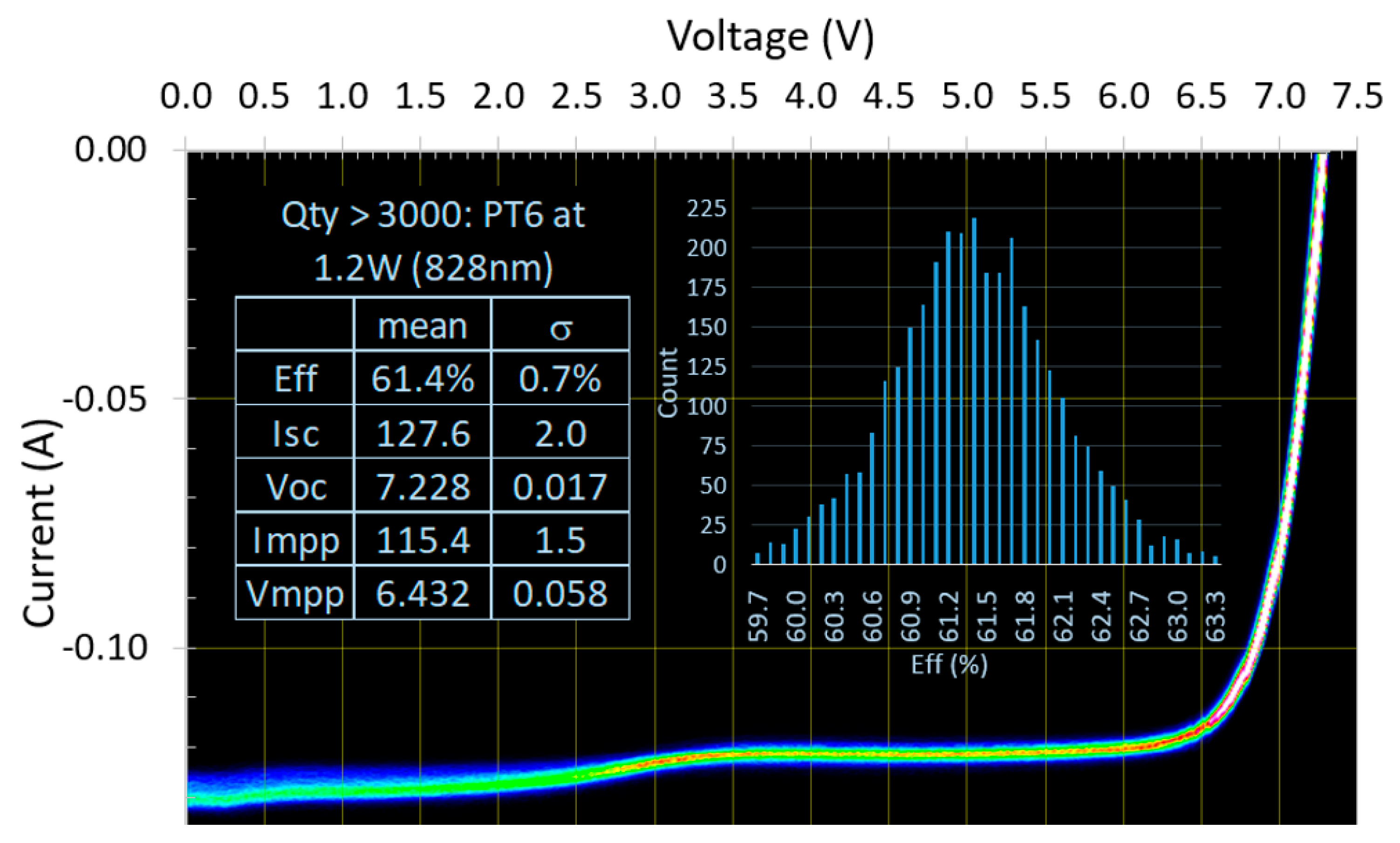
20], but in summary the quantum efficiency typically only decreases by a few percent on either side of the peak response, which is selected from the design parameters. The efficiency distribution at room temperature under 1.2 W of optical input power is shown in
Figure 1 for a production lot of devices packaged into an FC housing. The I-V curves display almost no series resistance (typically smaller than few tens of milliohms), and only about 10% of current drop between I
sc and I
mpp. The small current drop around a voltage of 3 V is ascribed to a small residual current mismatch at 808 nm, and similarly at 828nm as in
Figure 1. For this lot, the peak response is at about 815 nm, and at the optimal wavelength, the current drop between I
sc and I
mpp becomes minimal. A normal distribution is observed with an average OPC conversion efficiency value of Eff ~ 61%. Other key parameters measured at the maximum power point include the current, I
mpp = 115 mA, and the voltage, V
mpp = 6.43 V. The open circuit voltage is V
oc = 7.23 V.
Extended reliability testing was performed on these OPC devices with continuous illumination at 1.2 W at different temperatures for several thousands of hours. After a continuous 5000 h of stress-test aging with Pin ~ 1.2 W, we find that the performance of the aged devices is indistinguishable from the one of the control devices. No measureable performance deviations have been observed, thus confirming the high-reliability of the OPCs devices. The robustness of the devices stems from the single semiconductor epitaxy growth which eliminates the need for added complexity in the subsequent wafer fabrication process.
Product stability is a prerequisite for any of the selected optical power conversion strategies. The OPCs must be able to operate over a wide range of temperatures and input powers. Rigorous characterization and reliability testing were performed on all of Broadcom’s released products (AFBR-POCxxx product family) and all these OPC devices successfully completely passed the standard testing. This includes operation at various power levels and temperatures, temperature cycling (between −40 °C and 95 °C), temperature and humidity bias testing (85 °C/85% humidity), ESD (electrostatic discharge) tests, etc. More details about the device reliability are also found in the sections below.
3.2. Medium-Power, 800–830 nm Spectral Range
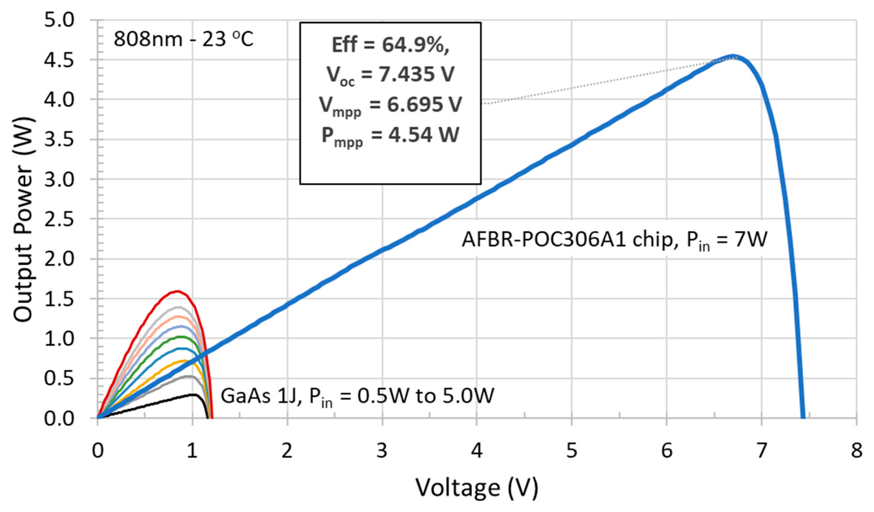
The results for Broadcom’s medium-power 6 V OPC chips are shown in
Figure 2. The power-voltage curve shows an efficiency of 64.9% at an input power of 7 W at 808 nm. Record output power values are obtained, here reaching P
mpp = 4.54 W. Other key parameters measured include I
mpp = 0.68 A, V
mpp = 6.695 V, and V
oc = 7.435 V. This gives a remarkable output voltage per subcell of 1.239 V. In other words, a very small bandgap voltage offset value of W
oc = (E
g/
q) − V
oc = 0.181 V is obtained, where E
g is here the bandgap of GaAs and
q is the electronic charge.
For direct comparison,
Figure 2 also shows the experimental results obtained with a GaAs single junction device (1J). The results are shown for the 1J for P
in between 0.5 W and 5 W. At P
in = 0.5 W, the 1J gives an efficiency of ~ 58.8% with a high fill-factor (FF) of ~ 84% at a reasonable optimal load of R
mpp ~ 3.4 Ohms. For input optical powers giving rise to photocurrent densities comparable to the PT6 operated at P
in = 7 W, the V
oc of the 1J device measured to be; V
oc = 1.18 V. Therefore, the bandgap voltage offset value is ~60 mV lower for the PT6 than the 1J operated under comparable current generating conditions. More importantly, as can be seen on
Figure 2, the maximum power point quickly recedes to lower voltages when the optical input power is increased on the 1J. This is due to resistive losses associated with the large current densities for the case of the 1J. At P
in = 5 W the efficiency of the 1J has degraded to Eff = 31.8% at the small external optimal load of only 0.4 Ohm.
For fiber-based applications, the OPC chips are assembled into a medium-power housing with a standard ST fiber connector to provide a solid lock-in connection (see picture in the inset of Figure 5 further below). The assembled medium-power OPC device is Broadcom’s AFBR-POC306A1, extending the power range capabilities of the regular-power OPCs discussed in
Section 3.1. The housing and the chip properties are designed to accept an optical input power of 6 W. The optical input power is typically transmitted over a multimode fiber, using a numerical aperture of NA~0.22. If necessary, the housing could be customized to other NA values, or future iterations could consider the incorporation of homogenizing or efficient coupling elements, as is sometimes used to improve sunlight and laser light collection efficiencies.
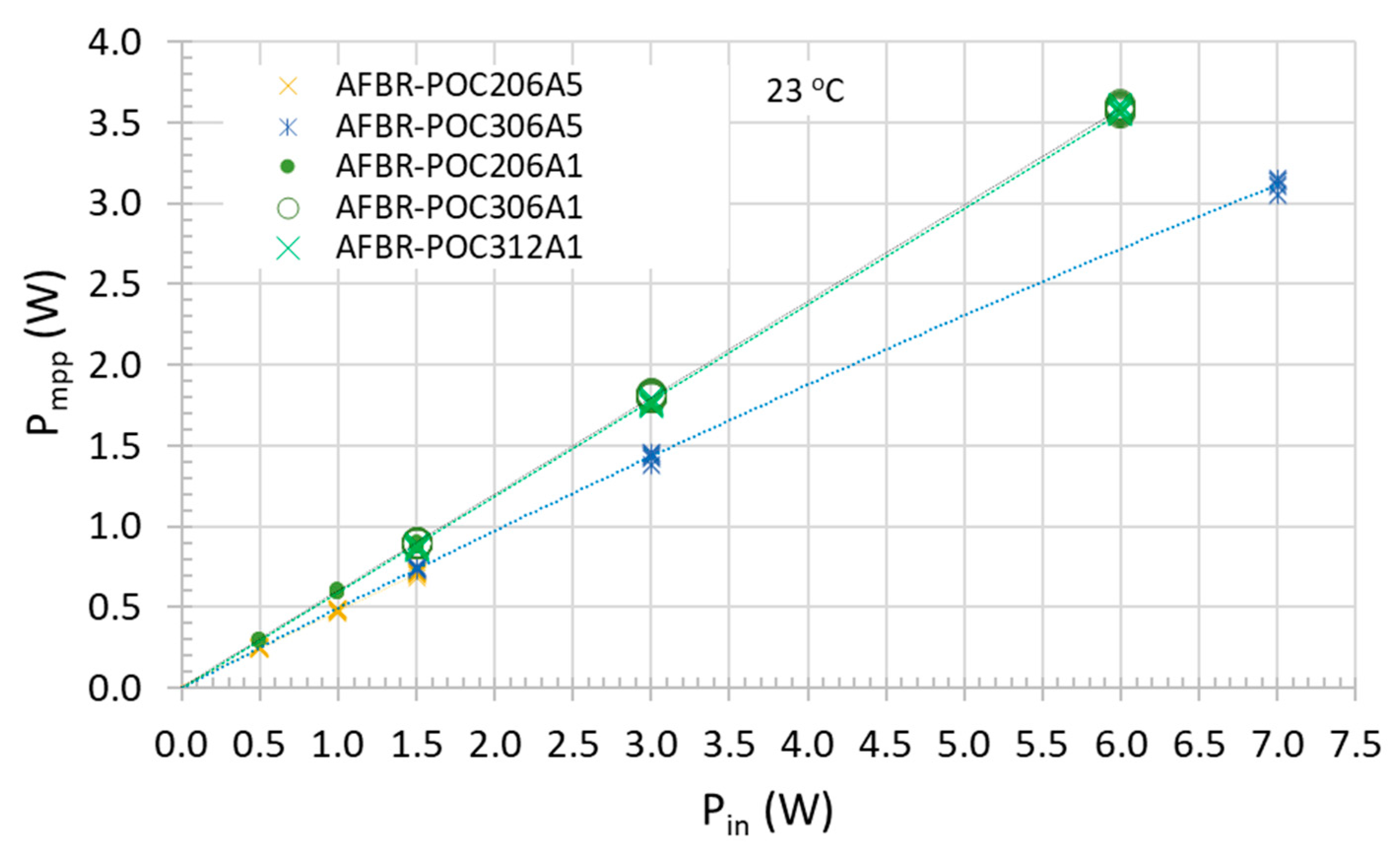
The output power vs. input power curve of the medium-power PT6 (AFBR-POC306A1) is shown in
Figure 3. A linear behavior is obtained up to P
in = 6 W, with a slope efficiency of 59.4%. As is also shown in
Figure 3, very similar results are obtained with the PT12 at 808 nm (Broadcom’s AFBR-POC312A1). It is also clear from
Figure 3 that the medium-power PT6 and the medium-power PT12 smoothly extend the power range of the regular-power PT6 (AFBR-POC206A1).
Figure 3 also shows the results for the 980 nm optical input: the medium-power AFBR-POC306A5 is also reaching an output power of P
mpp > 3 W, and is extending the power range of the regular-power AFBR-POC206A5 beyond P
in ~ 1.5 W.
More details about the 980 nm OPCs are also discussed in
Section 3.6 below, but it can be observed from
Figure 3 that AFBR-POC306A5 has a lower slope efficiency and a slight deviation from the linear relationship at higher optical powers. The latter is ascribed to some residual series resistance caused by non-optimized doping in the buffer layers of the structure. The somewhat lower conversion efficiency of the 980 nm OPC devices is at least in part attributable to the replacement of the GaAs absorber with an InGaAs absorber in the heterostructure design. We expect that further implementations and improvements of the 980 nm structure will result in OPC performance closer to the one observed with the 808 nm OPC devices. Moreover, the availability of higher power laser diodes at in the 980 nm spectral range more than compensate for the somewhat lower efficiency of the 980 nm OPCs.
The stability and reliability of the above OPC configuration and of other OPC options are further discussed in the following sub-section.
3.3. Stability and Reliability Properties
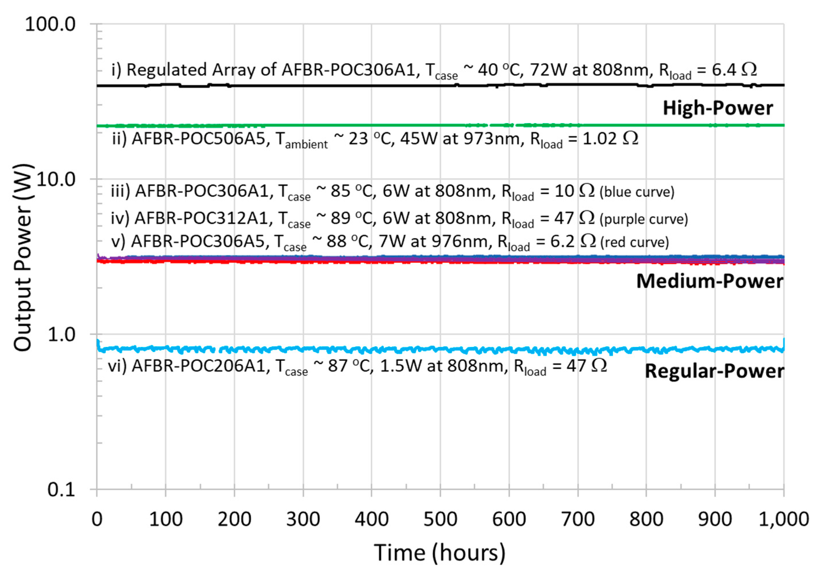
An example of measured stability and reliability is shown in
Figure 4 for OPC devices operating at various wavelengths and constant DC optical input power levels. In all cases, steady electrical outputs are obtained for extended periods of time. The characteristic properties of the OPCs (V
oc, I
sc, V
mpp, I
mpp, and Eff) remained the same for all the conditions and durations tested.
Figure 4 shows examples of six different OPC configurations: 960–980 nm 5 V OPCs for high-powers and medium-power (curve ii and v); 808 nm OPCs for medium-power 6 V (curve iii) and 12 V (curve iv), and regular-power 6 V (curve vi).
Figure 4 also shows that the medium-power OPCs can deliver ~3 W of stable electrical power when the case temperature is intentionally raised and kept at a temperature of 85 °C, as might be the case in harsh environments. Curve (iii), (iv), and (v) show the results for the options of an optical input at ~808 nm with output voltages of ~6 & 12 V and for an input at ~975 nm with ~6 V output. In addition, a practical optimal load R
mpp of ~47 Ω is obtained for both the regular-power PT6 and the medium-power PT12 of
Figure 4.
For power-over-fiber or optical wireless power transmission applications requiring even more useable power, an array of medium-power OPCs can deliver the required stable output. This is demonstrated with curve (i) (
Figure 4) showing the case of a 3 × 4 array giving a steady 40 W output power (i.e., using 3 parallel strings of 4 OPCs connected in series). The array of curve (i) uses a regulating electronic DC-DC down converter that had a conversion efficiency of 95.5% for the operating conditions used. The regulated output was set here to operate at a voltage of 16 V, giving an effective output load of 6.4 ohms. The 40 W array was also tested to be similarly stable when the DC-DC regulation was set at output voltages between 12 V and 20 V (not shown).
As mentioned in
Figure 2, the OPC results of
Figure 4 are remarkably different than the low-voltage and high currents typically obtained from single junction devices. Such a high current is generally less desirable because of the associated resistive losses, R
series*I
2 (where R
series is the parasitic series resistance from connecting wires, etc). In addition, as demonstrated above, the single junction approach reduces the optimal load to a few hundreds of mΩ for applications where high power is required. Such low load resistances are often unpractical. The latter will also be further demonstrated below in
Section 3.6 for the high-power OPCs.
3.4. Temperature and Output Voltage Properties
For most applications, the OPC devices must be able to operate over a wide range of temperatures and input powers.
Figure 5 shows the results of temperature behavior for the medium-power OPCs at an optical input power of P
in = 3 W and P
in = 6 W in (a) and P
in = 3 W and P
in = 7 W in (b).
Figure 5a shows the 808 nm response for the PT6 (Broadcom’s AFBR-POC306A1) and for the PT12 (Broadcom’s AFBR-POC312A1). The medium-power PT6 (Broadcom’s AFBR-POC306A5) is shown in
Figure 5b for the case of operation in the 960–990 nm range.
The results show that the conversion efficiency is remarkably high, reaching a maximum Eff > 64% for both the PT6 and the PT12 at 808 nm. The measured performance for optical-to-electrical conversion remains strong even at the higher operating temperatures, yielding output power capabilities in excess of 3 W at all temperatures for the 808 nm OPCs, and just slightly lower for the 980 nm OPCs.
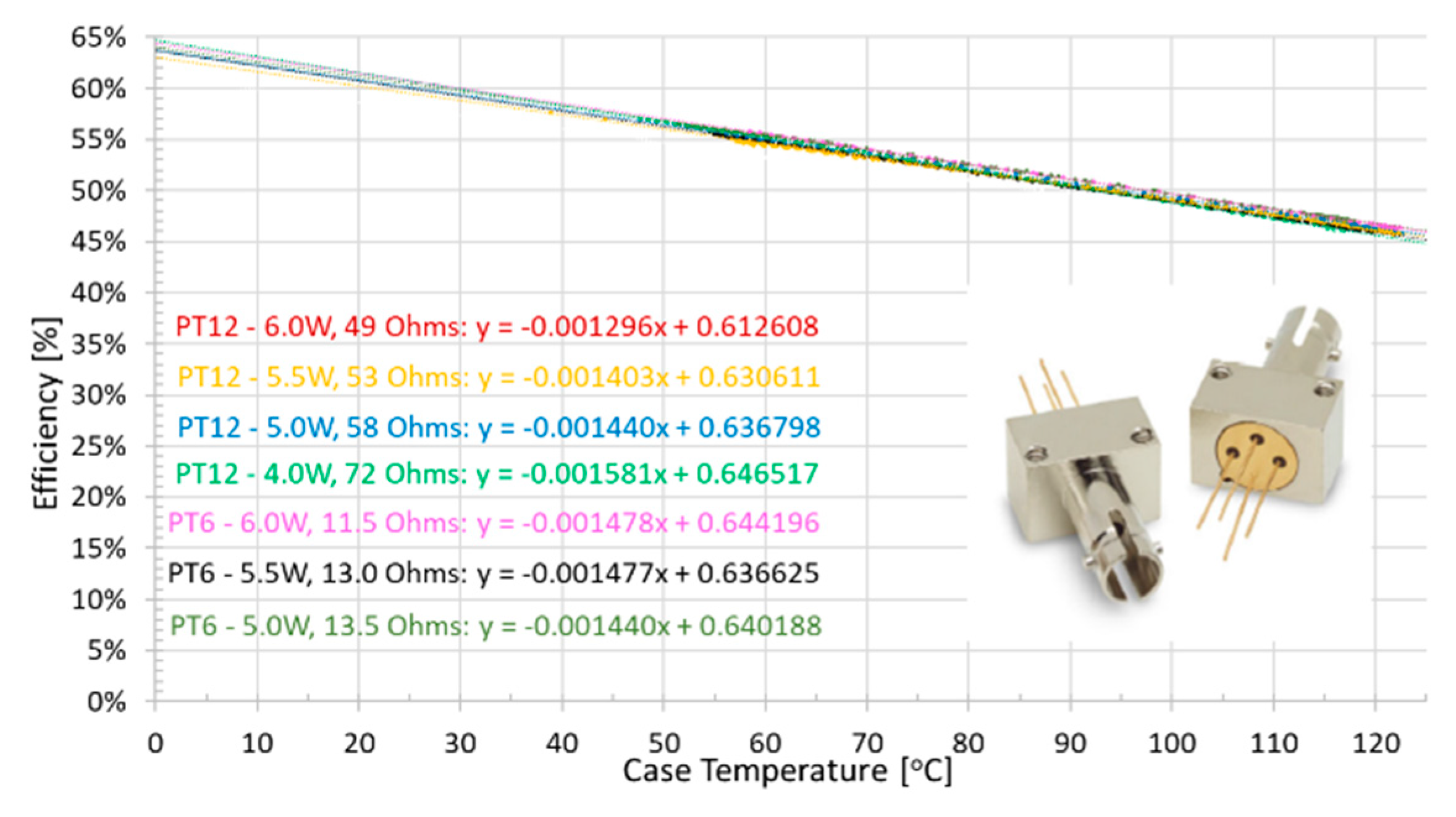
To understand the OPC performance in field operation, it is necessary to: (1) determine the temperature coefficients of the key parameters of the OPCs and (2) evaluate the expected or actual OPC case temperature given the environment and the thermal management used for the OPC device. This includes parameters such as the ambient temperature, the design options regarding the size of the heatsink used and the system case configuration, the airflow values, etc. The thermal management aspects and the operating temperature will vary from system to system depending on the system design, but the temperature coefficients are uniquely determined and can be extracted from the measured temperature dependence of the OPC devices. For example, the temperature coefficients can be assessed from the linear region of the data in the high temperature range.
Figure 6 shows the results for both the PT6 and the PT12 medium-power devices at different input powers. It is found that both, the AFBR-POC306A1 and the AFBR-POC312A1 have very similar conversion efficiencies with a temperature coefficient of about −0.14%abs/°C. The results of
Figure 6 were obtained in steady-state DC conditions using a fixed load. The optimal load impedance varies with the input power and is different for PT6 vs. PT12. However, as can be deduced in
Figure 6, the optimal load has a relatively small dependence on the temperature.
Figure 6 therefore confirms, using a DC fixed load method, that for medium-power PT6 and PT12 at 808 nm for 4 W < P
in < 6 W, efficiencies greater than 50% are obtained for T < 90 °C. These results illustrate that, for typical operating conditions, the photon recycling effect, inherent in VEHSA based devices, contributes significantly to overall favorable spectral and temperature behaviors [
20,
21,
22,
23].
3.5. Benefits of Multijunctions and Optical-to-Electrical Conversion at Higher Output Voltages
Figure 7 compares the performance of medium-power OPCs for P
in = 6 W. Results for a PT12, a PT6, and a single junction device are shown. The solid lines are obtained from the measured or projected I-V curves, as indicated in the figure caption. The small black crosses are obtained from fixed load steady-state testing, similar to the measurements described above in
Figure 4 and
Figure 6. For an optical input power of 6 W at 808 nm, the PT12 and PT6 both reach Eff ~ 60% at a practical optimal load values of 47.0 and 11.8 ohms, respectively. By contrast, the high-current and low-voltage outputs of the single junction device lead to an optimal impedance load of only a few hundreds of milliohms. Most electronic circuits are not designed to operate at such low values of voltage and load, resulting in high I
2R
s losses. In practice, it is particularly of concern with single-junction devices when considering the typical series resistance from wires and inter-connections, which can become a significant fraction of such a low optimal load value. Simply put, multijunction OPCs are more advantageous as power sources for practical applications and are clearly more advantageous to yield good efficiencies as the input power becomes larger.
Evidently, the vertical multijunction approach is very effective at tailoring the output voltage and the optimal load. To further exemplify this aspect,
Figure 8 demonstrates the case for a PT30 VEHSA device (Broadcom’s AFBR-POC230A1). It is featuring an output voltage of >35 V in a load of 802 Ω at an optical input power of 5.5 W (averaged optical intensity of 170 W/cm
2). It is by far the highest output voltage reported for an optical-to-electrical conversion using a single device and with such a high output power. The previous record value for the highest output voltage was reported for a PT20 structure with a V
oc > 23 V [
7].
It should be noted that the results for
Figure 8 are obtained with a fixed resistive load value (here 802 Ω). The load value was chosen to be near the optimal value (i.e., R
mpp) for an input power of 5.5 W. Consequently, as expected the output voltage increases smoothly with increasing optical input powers, up to a maximum value of V
mpp~ 35 V when the input power reaches 5.5 W. For that fixed load of 802 Ω the maximum output power reaches P
mpp ~ 1.5 W, yielding a conversion efficiency of 27%. Increasing the input power to values higher than 5.5 W (not shown) results in a saturation of the output voltage and a decrease in efficiency, as expected. The efficiency is relatively low for this implementation of the PT30 because it is not yet optimized and it was designed for an input wavelength near the GaAs band-edge, significantly away from the optical input of 808 nm used in the measurements of
Figure 8.
More importantly, the results of
Figure 8 give an example in pulsed operation mode, here using a 5% duty-factor. Some applications can benefit from operating in fast response or pulse-width modulated mode. While the results presented in this study are obtained with devices that were not specifically optimized for fast response times, we expect that further straightforward device design optimizations could readily be implemented to favor fast response times and will be the topic of future studies.
As another example of single-junction devices, Broadcom designed and fabricated prototypes of InGaAs OPCs for the other important spectral range of 1500–1600 nm. These OPCs exhibited a remarkable electrical output power of P
mpp > 0.5 W with a conversion efficiency of Eff ~ 36% at 1550 nm with an optimal load of ~ 0.3 Ohm [
5]. Similar to the example shown above, we expect that devices based on the multijunction InGaAs VEHSA design would exhibit increased optimal loads and improved operating characteristics. Given the importance of the ~1550 nm wavelength range for optical communication applications, it suggests such further developments will be of key interest.
3.6. High-Power Capabilites and OPCs for the 960–980 nm Spectral Range
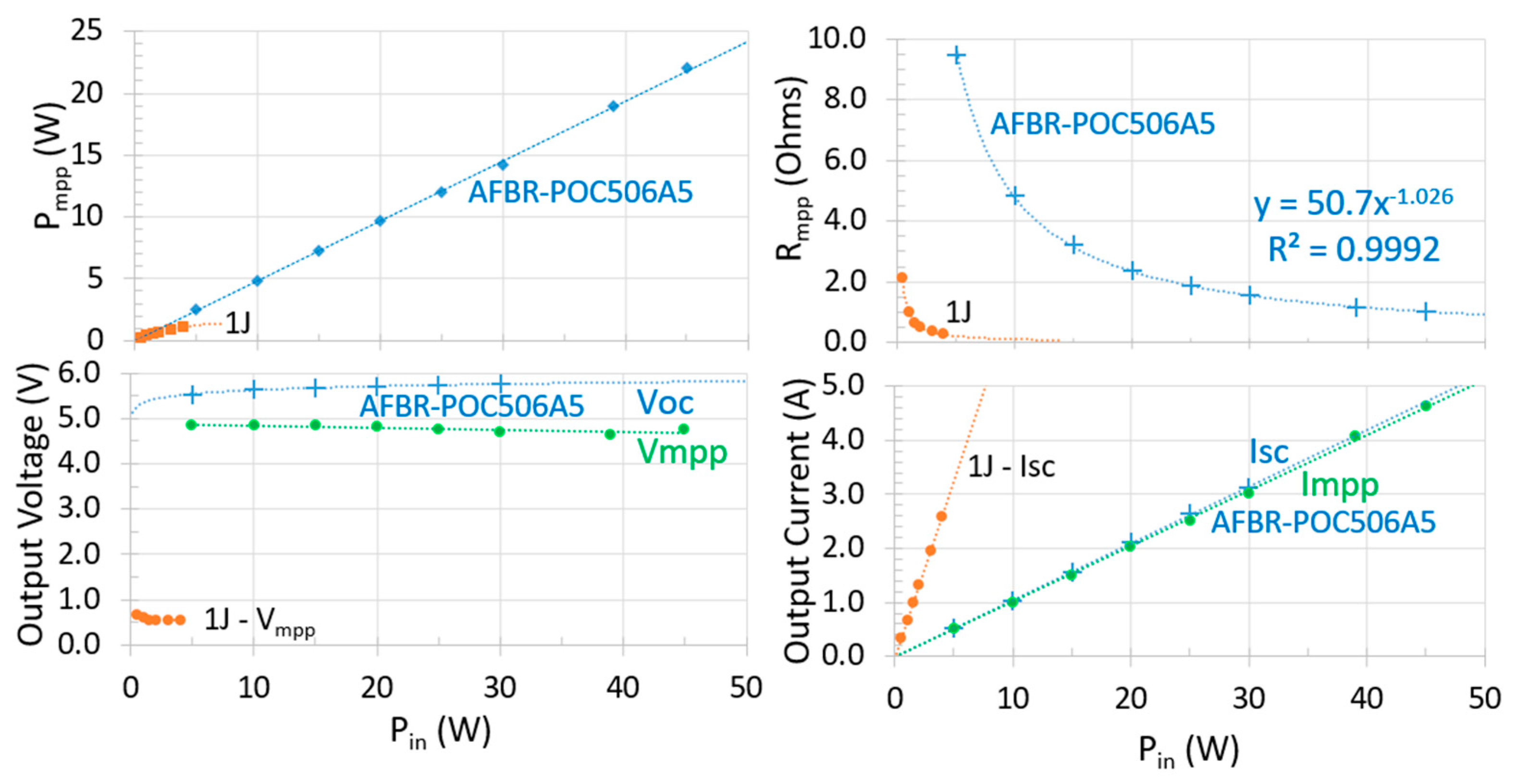
In
Figure 4, the steady-state fixed-load measurements for the high-power 980 nm OPC demonstrated very stable operation with over 20 W of output power for extended continuous times (curve ii). To study in more detail the properties and capabilities of the high-power multijunction OPCs,
Figure 9 shows the input power dependence of the key performance parameters of such a PT6 device for the 960–980 nm spectral range (Broadcom’s AFBR-POC506A5). For the range up to almost 50 W of optical input power, the P
mpp vs. P
in relationship is found to have negligible deviations from a linear regression (the output power is taken as P
mpp). The output voltage (V
mpp) remains over 4.5 V for the entire range, while the output current (I
mpp) increases linearly to 5 A at slightly below P
in = 50 W. The resulting optimal load decreases with the regression R
mpp = 50.7/
Pin1.026, with P
in in Watts and R
mpp in Ohms.
For comparison purposes,
Figure 9 also shows the measured data obtained under the same conditions with a single junction (1J) InGaAs OPC (orange color curves). Clearly, the performance of the 1J device is severely limited compared to the PT6 OPCs: output powers much in excess of 1 W are not feasible because of the very large photocurrent that the 1J needs to generate and extract under these conditions. The optimal external load quickly collapses to just a few hundred milliohms and makes the 1 J design not suitable.
The thinner subcells of the multijunction design can help to maintain a good conversion efficiency in situations for which the minority photo-carrier lifetime can be reduced because of higher defect densities and higher non-radiative recombination rates. Clearly, in
Figure 9 and previously in
Figure 3,
Figure 4 and
Figure 5, high conversion efficiencies are obtained, therefore demonstrating that the multijunction InGaAs OPCs can be used for the 960–990 nm spectral range. The latter spectral range is typically only accessible with semiconductor absorbers that are less ideal than binary GaAs, for example. Therefore, the multijunction design is even more attractive for the long-wavelength OPCs.
For the results in the above figures, it should also be noted that the high conversion efficiency is maintained for average optical intensities up to ~50 W/cm
2. In addition, we observed that at these intensities there are significant margins of operation. For example, the optical input (optical spot) can be set to be under-filling the OPC’s active area by a factor of 2 without significantly affecting the measured performance. Furthermore, the optical spot has been measured to have a flat-top/Gaussian profile with peak intensity that can be 2× higher than the average beam intensity. Therefore, it confirms that the tunnel junctions in these InGaAs mutlijunction OPCs can sustain optical intensities up to 200 W/cm
2 [
26].
From years of developments in other industries, high-power 980 nm laser diodes have become highly reliable, with one of the lowest
$/W metrics and long lifetimes [
27]. Therefore, the high-power and long-wavelength OPC results obtained here demonstrate that many new applications could benefit from galvanic isolated power with unprecedented output levels.
4. Discussion
We have demonstrated that multijunction optical power converters are significantly more advantageous than their single-junction predecessors, both for a better conversion efficiency and for their ability to operate in a more practical voltage and load impedance range. By design, the multijunction configuration operates with thinner base layers. The layers are thin compared to the photocarrier diffusion length and this favors more efficient minority carrier extraction and consequently slightly higher output voltages. For example, a small bandgap voltage offset of 0.181 V is measured for a GaAs PT6 structure with an optical input of 7 W at 808 nm (48.5 W/cm
2). The maturity of the GaAs material system and the multijunction design enables record conversion efficiencies (Eff = 64.9%) at record output powers (P
mpp = 4.54 W) for room temperature operation (
Figure 2).
Even higher conversion efficiencies could be obtained by reducing the energy difference between the photons of the optical input and the absorber bandgap. For practical operation, however, the devices need to work efficiently over a significant temperature range and it is therefore more appropriate to select an optical input at a wavelength not too close to the absorber band-edge. Moreover, given the commercial laser diode availability, a design wavelength of 808 nm is particularly attractive for regular-power (Pmpp < 1 W) and medium-power (Pmpp < 3 W) power-over-fiber or optical wireless power transmission applications. In additional developments, the thickest base of the multijunction OPCs could be made even thinner by incorporating Bragg reflectors below the absorber region. Such additional developments could notch up the conversion efficiency of multijunction OPCs in the future. Clearly, additional optical measurements (e.g., detailed investigations of the index of refractions and absorption coefficients) and additional modeling (e.g., to accurately account for the impact of photon coupling and recycling) can continue to improve the understanding of the multijunction OPC devices and could further increase the champion device efficiencies.
No device performance degradation has been observed for extended operations under high optical input powers and operating device temperatures of T > ~85 °C.
Figure 4 shows stable results up to 1000 h of operation for all the different device configurations. We found that additional extended reliability testing of groups of such OPCs, for many thousands of hours, still did not display measureable performance degradations. The expected device lifetime is therefore obviously long, but we cannot extract a degradation activation energy from the data obtained at this time. This is mainly because the reliability testing is normally performed in accordance to the normal operating range (e.g., temperatures up to < 100 °C). Studies with higher temperatures, longer durations, and larger sample sizes should help to obtain the activation energy. More reliability testing at higher temperatures could therefore be performed in the future to try to extract the activation energy and mean time before failure data.
For medium-power operation (P
in < 6 W), the PT6 and the PT12 have very similar performance over the entire operating range, with a temperature coefficient of only ΔEff/ΔT ~ −0.14abs%/°C. The main difference between the two OPCs is that the PT12 has the advantage of offering an optimal load R
mpp about 4× larger because it runs at about ½ the output current and 2x the output voltage (as seen in
Figure 5,
Figure 6 and
Figure 7). For the chosen design, the performance peaks at a device operating temperature of T
case ~ −20 °C, but we expect this could be shifted to higher temperatures by adjusting the details of the design parameters.
For operation at longer wavelengths in the 1500–1600 nm range, the bandgap of the semiconductor absorber is relatively small and therefore yields lower output voltages. Consequently, it will become essential to implement multijunction architectures for the longer input wavelength OPCs in order to offer practical and readily useable solutions in systems’ architecture. The measured InGaAs single junction devices with a conversion efficiency of Eff = 36% at an output of Pmpp > 0.5 W support that the future multijunction 1550 nm OPCs can have very attractive performance and a much improved optimal load compared to the Rmpp ~ 0.3 Ohm obtained with the single junction devices.
5. Conclusions
Optical power converters enable new and promising power-over-fiber or power beaming applications. Here, we have exemplified opportunities for various power options. Stable and reliable DC electrical outputs have been demonstrated with record efficiencies and for output power of up to Pmpp = 40 W. We have shown the various options currently available and the ongoing device developments for the 800–830 nm, 960–990 nm, and 1500–1600 nm spectral ranges. These high-efficiency multi-junction designs enable practical optimal loads and tailored output voltages.
Additional improvements of the optical to electrical conversion efficiencies are possible in future studies by further optimizing the heterostructure design to the various optical spectrum of interest. For example, this can be achieved by extracting more precisely the optical constants of the absorber material and by quantifying more accurately the impact of photon coupling and recycling in the different subcells. Higher OPC efficiencies can also be readily achieved by minimizing the thermalization losses by reducing the energy difference between the photons of the optical input and the absorber bandgap.
Author Contributions
Conceptualization, all; methodology, all; software, S.F. and D.M.; validation, S.F., D.M., J.L. and T.-C.W.; formal analysis, S.F. and D.M.; investigation, S.F. and D.M.; data curation, S.F. and D.M.; writing—original draft preparation S.F.; writing—review and editing S.F., D.M., and J.-G.W.; visualization, S.F.; project administration, S.F., D.M., C.P., B.L., J.W., and M.W.; funding acquisition, J.W., and M.W. All authors have read and agreed to the published version of the manuscript.
Funding
This research received no external funding.
Data Availability Statement
The data that support the findings of this study are available from the corresponding author upon reasonable request.
Conflicts of Interest
The authors declare no conflict of interest.
References
- Matsuura, M.; Nomoto, H.; Mamiya, H.; Higuchi, T.; Masson, D.; Fafard, S. Over 40-W Electric Power and Optical Data Transmission Using an Optical Fiber. IEEE Trans. Power Electron. 2020, 36, 4532. [Google Scholar] [CrossRef]
- Helmers, H.; Armbruster, C.; von Ravenstein, M.; Derix, D.; Schöner, C. 6-W Optical Power Link with Integrated Optical Data Transmission. IEEE Trans. Power Electron. 2020, 35, 7904. [Google Scholar] [CrossRef]
- Jaffe, P.; Jenkins, P.; Nugent, T. Energy Transmitted by Laser in ‘Historic’ Power-Beaming Demonstration. Available online: https://youtu.be/Xb9THqrXd4I (accessed on 22 October 2019).
- Wilkins, M.; Ishigaki, M.; Provost, P.-O.; Masson, D.; Fafard, S.; Valdivia, C.E.; Dede, E.M.; Hinzer, K. Ripple-free boost-mode power supply using photonic power conversion. IEEE Trans. Power Electron. 2018, 34, 1054. [Google Scholar] [CrossRef]
- Fafard, S.; Masson, D.; Werthen, J.G.; Ono, M.; Liu, J.; Wu, T.C.; Hundsberger, C.; Schwarzfischer, M.; Steinle, G.; Gaertner, C.; et al. Photovoltaic power converters and application to optical power transmission. In Proceedings of the 2nd Optical Wireless and Fiber Power Transmission Conference (OWPT2021), Yokohama, Japan, 21–23 April 2021. [Google Scholar]
- Fafard, S.; York, M.C.; Proulx, F.; Valdivia, C.E.; Wilkins, M.M.; Arès, R.; Aimez, V.; Hinzer, K.; Masson, D.P. Ultrahigh efficiencies in vertical epitaxial heterostructure architectures. Appl. Phys. Lett. 2016, 108, 071101. [Google Scholar] [CrossRef]
- Fafard, S.; Proulx, F.; York, M.C.; Richard, L.S.; Provost, P.O.; Arès, R.; Aimez, V.; Masson, D.P. High-photovoltage GaAs vertical epitaxial monolithic heterostructures with 20 thin p/n junctions and a conversion efficiency of 60%. Appl. Phys. Lett. 2016, 109, 131107. [Google Scholar] [CrossRef]
- Helmers, H.; Lopez, E.; Höhn, O.; Lackner, D.; Schön, J.; Schauerte, M.; Schachtner, M.; Dimroth, F.; Bett, A.W. 68.9% Efficient GaAs-Based Photonic Power Conversion Enabled by Photon Recycling and Optical Resonance. Phys. Status Solidi (RRL) Rapid Res. Lett. 2021, 15, 2100113. [Google Scholar] [CrossRef]
- France, R.M.; Buencuerpo, J.; Bradsby, M.; Geisz, J.F.; Sun, Y.; Dhingra, P.; Lee, M.L.; Steiner, M.A. Graded buffer Bragg reflectors with high reflectivity and transparency for metamorphic optoelectronics. J. Appl. Phys. 2021, 129, 173102. [Google Scholar] [CrossRef]
- Beattie, M.N.; Valdivia, C.E.; Wilkins, M.M.; Zamiri, M.; Kaller, K.L.C.; Tam, M.C.; Kim, H.S.; Krich, J.J.; Wasilewski, Z.R.; Hinzer, K. High current density tunnel diodes for multi-junction photovoltaic devices on InP substrates. Appl. Phys. Lett. 2021, 118, 062101. [Google Scholar] [CrossRef]
- Wagner, L.; Reichmuth, S.K.; Philipps, S.P.; Oliva, E.; Bett, A.W.; Helmers, H. Integrated series/parallel connection for photovoltaic laser power converters with optimized current matching. Prog. Photovolt. Res. Appl. 2020, 29, 172. [Google Scholar] [CrossRef]
- Panchak, A.; Khvostikov, V.; Pokrovskiy, P. AlGaAs gradient waveguides for vertical p/n junction GaAs laser power converters. Opt. Laser Technol. 2021, 136, 106735. [Google Scholar] [CrossRef]
- Lin, M.; Sha, W.E.I.; Zhong, W.; Xu, D. Intrinsic losses in photovoltaic laser power converters. Appl. Phys. Lett. 2021, 118, 104103. [Google Scholar] [CrossRef]
- Zhao, Y.; Li, S.; Ren, H.; Li, S.; Han, P. Energy band adjustment of 808 nm GaAs laser power converters via gradient doping. J. Semicond. 2021, 42, 032701. [Google Scholar] [CrossRef]
- Nouri, N.; Valdivia, C.E.; Beattie, M.N.; Zamiri, M.S.; Krich, J.J.; Hinzer, K. Ultrathin monochromatic photonic power converters with nanostructured back mirror for light trapping of 1310-nm laser illumination. In Physics, Simulation, and Photonic Engineering of Photovoltaic Devices X; International Society for Optics and Photonics: Bellingham, WA, USA; Volume 116810X.
- Komuro, Y.; Honda, S.; Kurooka, K.; Warigaya, R.; Tanaka, F.; Uchida, S. A 43.0% efficient GaInP photonic power converter with a distributed Bragg reflector under high-power 638 nm laser irradiation of 17 W cm−2. Appl. Phys. Express 2021, 14, 052002. [Google Scholar] [CrossRef]
- Masson, D.; Proulx, F.; Fafard, S. Pushing the limits of concentrated photovoltaic solar cell tunnel junctions in novel high-efficiency GaAs phototransducers based on a vertical epitaxial heterostructure architecture. Prog. Photovolt. Res. Appl. 2015, 23, 1687. [Google Scholar] [CrossRef] [Green Version]
- Fafard, S.; Masson, D.P. Transducer to Convert Optical Energy to Electrical Energy. U.S. Patent 9,673,343, 6 June 2017. [Google Scholar]
- Fafard, S.; York, M.C.A.; Proulx, F.; Wilkins, M.; Valdivia, C.E.; Bajcsy, M.; Ban, D.; Arès, R.; Aimez, V.; Hinzer, K.; et al. Ultra-efficient N-junction photovoltaic cells with Voc > 14 V at high optical input powers, PVSC 2016. In Proceedings of the IEEE 43rd Photovoltaic Specialists Conference, Portland, OR, USA, 5–10 June 2016; p. 2374. [Google Scholar]
- Proulx, F.; York, M.C.A.; Provost, P.O.; Arès, R.; Aimez, V.; Masson, D.P.; Fafard, S. Measurement of strong photon recycling in ultra-thin GaAs n/p junctions monolithically integrated in high-photovoltage vertical epitaxial heterostructure architectures with conversion efficiencies exceeding 60%. Phys. Status Solidi RRL 2017, 11, 1600385. [Google Scholar] [CrossRef]
- Wilkins, M.; Valdivia, C.E.; Gabr, A.M.; Masson, D.; Fafard, S.; Hinzer, K. Luminescent coupling in planar opto-electronic devices. J. Appl. Phys. 2015, 118, 143102. [Google Scholar] [CrossRef] [Green Version]
- Lopez, E.; Höhn, O.; Schauerte, M.; Lackner, D.; Schachtner, M.; Reichmuth, S.K.; Helmers, H. Experimental coupling process efficiency and benefits of back surface reflectors in photovoltaic multi-junction photonic power converters. Prog. Photovolt. Res. Appl. 2021, 29, 461. [Google Scholar] [CrossRef]
- Xia, D.; Krich, J.J. Efficiency increase in multijunction monochromatic photovoltaic devices due to luminescent coupling. J. Appl. Phys. 2020, 128, 013101. [Google Scholar] [CrossRef]
- Kimovec, R.; Helmers, H.; Bett, A.W.; Topič, M. Comprehensive electrical loss analysis of monolithic interconnected multi-segment laser power converters. Prog. Photovolt. Res. Appl. 2019, 27, 199. [Google Scholar] [CrossRef]
- Kimovec, R.; Helmers, H.; Bett, A.W.; Topič, M. On the Influence of the Photo-Induced Leakage Current in Monolithically Interconnected Modules. IEEE J. Photovolt. 2018, 8, 541–546. [Google Scholar] [CrossRef]
- Fafard, S.; Masson, D.P. Transducer to Convert Optical Energy to Electrical Energy. U.S. Patent 10,158,037, 18 December 2018. [Google Scholar]
- Yamagata, Y.; Yamada, Y.; Kaifuchi, Y.; Nogawa, R.; Morohashi, R.; Yamaguchi, M. Performance and reliability of high power, high brightness 8xx-9xx nm semiconductor laser diodes. In Proceedings of the 2015 IEEE High Power Diode Lasers and Systems Conference (HPD), Coventry, UK, 14–15 October 2015; pp. 7–8. [Google Scholar] [CrossRef]
Figure 1.
Performance of regular-power PT6 from a group of over 3000 devices (Broadcom’s AFBR-POC206A1). Measured at room temperature (T ~ 23 °C) with an input power of 1.2 W at 828 nm. The chip area is 0.03 cm2, giving an average optical input intensity of 37 W/cm2 at 1.2 W. Histogram and statistics are shown in the insets. The density plot of all the current-voltage (I-V) curves is traced using a rainbow color scheme (cold colors correspond to lower occurrence points and hot colors correspond to higher occurrence points).
Figure 2.
Power–voltage results of Broadcom’s medium-power PT6 chips measured at an optical input power of Pin = 7 W at 808 nm (blue curve). The chip area is 0.14 cm2, giving an average optical intensity of 48 W/cm2 at 7 W. The multiple curves near 1 V are obtained with a single junction GaAs OPC measured with an optical input power between 0.5 W (black curve with Eff = 58.8%) and 5.0 W (red curve with Eff = 31.8%).
Figure 3.
OPCs’ output power vs. optical input power curves for the regular-power (AFBR-POC206A1 and AFBR-POC206A5) and medium-power (AFBR-POC306A1, AFBR-POC312A1, and AFBR-POC306A5). The “A1” and “A5” devices are designed for, and measured at, an optical input wavelength of ~808 nm and ~975 nm respectively.
Figure 4.
Stability measurement, in DC steady-state operation, of Broadcom’s photovoltaic OPCs covering various power, voltage, and spectral range options. The test conditions are indicated on the plot, where Tcase is the measured case temperature and Rload is the fixed output resistor used. The high-power AFBR-POC506A5 OPCs have an area of 1 cm2, giving an average optical input intensity of 45 W/cm2 at 45 W.
Figure 5.
Temperature dependence of the output power for the medium-power OPCs for spectral range option of 800–830 nm in (a), and for 960–990 nm in (b). Test details are indicated on the plot. The average optical intensities are 20.8, 41.6, and 48.5 W/cm2 for the Pin of 3 W, 6 W, and 7 W respectively.
Figure 6.
Measured temperature behavior for medium-power PT6 and PT12 OPC devices at λin ~ 808 nm. At Pin = 6 W (average optical intensity of 41.6 W/cm2), output powers greater than 3 W are obtained for T < 90 °C. The temperature coefficients are extracted from a linear fit to the measured data. The test conditions and linear regression results are indicated on the plot. Inset: picture of the medium-power OPCs.
Figure 7.
Performance vs. output load resistance for medium-power OPCs for Pin = 6 W (average optical intensity of 41.6 W/cm2) for a PT12, a PT6, and a single junction device. Solid lines from I-V curves and crosses are from fixed-load testing.
Figure 7.
Performance vs. output load resistance for medium-power OPCs for Pin = 6 W (average optical intensity of 41.6 W/cm2) for a PT12, a PT6, and a single junction device. Solid lines from I-V curves and crosses are from fixed-load testing.
Figure 8.
Regular-power PT30 (Broadcom’s AFBR-POC230A1) in pulsed mode at 808 nm with duty-factor of DF = 5% in a fixed external load of 802 Ohms. The device area is 0.03 cm2, giving an averaged optical intensity of 170 W/cm2 at 5.5 W.
Figure 8.
Regular-power PT30 (Broadcom’s AFBR-POC230A1) in pulsed mode at 808 nm with duty-factor of DF = 5% in a fixed external load of 802 Ohms. The device area is 0.03 cm2, giving an averaged optical intensity of 170 W/cm2 at 5.5 W.
Figure 9.
Input power dependence of the key performance parameters of the high-power PT6 OPC (Broadcom’s AFBR-POC506A5) at an input laser wavelength of ~ 977 nm at T = 23 °C. The results for a 1J InGaAs OPC measured at 977 nm are also shown for comparison (orange curves). The OPCs’ active areas are 1 cm2 in all cases.
| Publisher’s Note: MDPI stays neutral with regard to jurisdictional claims in published maps and institutional affiliations. |
© 2021 by the authors. Licensee MDPI, Basel, Switzerland. This article is an open access article distributed under the terms and conditions of the Creative Commons Attribution (CC BY) license (https://creativecommons.org/licenses/by/4.0/).

