
Comparative Simulations of Conductive Nitrides as Alternative Plasmonic Nanostructures for Solar Cells


1
Institute of Condensed Matter Theory and Optics, Abbe Center of Photonics, Friedrich-Schiller-Universität Jena, 07743 Jena, Germany
2
International Solar Energy Research Center Konstanz, Rudolf-Diesel-Straße 15, 78467 Konstanz, Germany
*
Author to whom correspondence should be addressed.
Energies 2021, 14(14), 4236; https://doi.org/10.3390/en14144236
Submission received: 17 May 2021
/
Revised: 7 July 2021
/
Accepted: 7 July 2021
/
Published: 14 July 2021
(This article belongs to the Special Issue Analysis and Numerical Modeling in Solar Photovoltaic Systems)
Abstract
:Particle layers employing conductive transition metal nitrides have been proposed as possible alternative plasmonic materials for photovoltaic applications due to their reduced losses compared to metal nanostructures. We critically compare the potential photocurrent gain from an additional layer made of nanopillars of nitrides with other material classes obtained in an optimized c-Si baseline solar cell, considering an experimental doping profile. A relative photocurrent gain enhancement of on average 5% to 10% is observed, achieving for a few scenarios around 30% gain. The local field enhancement is moderate around the resonances for nitrides which spread over the whole ultraviolet and visible range. We can characterize two types of nitrides: nitrides for which the shading effect remains a problem similar to for metals, and others which behave like dielectric scatterers with high photocurrent gain.
1. Introduction
Exploiting plasmonic effects for solar cells [1,2] has not led to the substantial improvement of photovoltaic (PV) technologies that the scientific community developing regenerative energy devices once believed. Layers of nanosized particles and nanostructured surfaces such as one-dimensional gratings [3] and two-dimensional particle layers [4] enable efficient forward scattering of incident light, increasing the optical path length and thus the exposure of an underlying photo-active region to photons [5]. Thus, research efforts have concentrated on additional nanostructured layers to further optimize the light trapping and management [6] either as front layers [7,8], back reflectors [9,10] or dispersed within the antireflection coating [11]. Moreover, metal nanoparticles can yield high local fields close to the resonant oscillation of their free conduction band electrons, the plasmon excitation. This has, in particular, raised interest for plasmon-assisted enhancement of processes within the solar cell device [12], either via a direct increase in the charge carrier generation or indirectly through energy conversion effects such as photoluminescence [13,14] with either quantum dots [15] or embedded nanoparticles [16,17]. However, metals struggle with high Ohmic losses that their supportive effects cannot sufficiently counteract and the directivity of the scattered light depends strongly on the control over the particle shape [18,19,20]. In recent years, conductive transition metal nitrides have been proposed as alternative plasmonic materials, allowing for resonant field enhancement effects while at the same time being less absorptive over a broad range of the spectrum [21,22,23]. Fabrication processes and studies to integrate these materials for PV applications are in place [24].
Nanostructured layers as extra components to photovoltaic devices face another difficulty. Even commercially available baseline solar cells are already highly optimized. The Solar cell efficiency tables Ref. [25] record the highest photocurrent measured for n-type c-Si integrated back contact (IBC) systems at mA/cm (efficiency of ), while thin-film modules achieve mA/cm (efficiency of ). With this in mind, nanostructured layers need to add a convincing amount to the photocurrent or overall efficiency. The main challenges in modeling complex solar cells are the (i) integrated electro-optical modeling [26] and the (ii) impact of localized quantum effects at nanoscale features [27,28].
(i) Commercially available software for photovoltaic devices concentrates on electronic properties of the device structure and cannot fully address optically induced effects stemming from light-matter interaction with nanoparticles (NPs). Scattering of light, plasmonic and coupling effects cannot be fully captured when optical phenomena are reduced to raytracing instead of wave propagation and quasistatic fields neglecting thus retardation effects over the large-scale device. Within computational nanophotonics, a wealth of analytic and numerical tools are available to describe the optical properties of nanoparticles, including arbitrary shapes [29,30,31,32], particle clusters [33], two-dimensional particle arrays [34,35], including random distributions [4], rough surface morphologies [36,37], as well as three-dimensional photonic crystal structures [38].
(ii) Standard optical modeling, on the other hand, does neglect mesoscopic electron dynamics in highly doped semiconductors and metal nanostructures and the relevance of quantum corrections in PV devices was shown in our previous works [35,39,40,41,42]. Though such effects are highly localized and short-ranged, optical coupling can lead to mediating their impact on the overall device performance via retardation effects [43,44] in a large-scale, patterned structure. In particular, the strong optical coupling of metal nanofeatures with Si substrates needs to be considered beyond classical electrodynamics [45]. The advantage of employing semi-classical theories is their mostly analytic formulation and thus compatibility with existing numerical procedures for improved electro-optical simulations.
In this article, we compare the relative photocurrent gain obtained with nanopillar layers made of metals, nitrides and dielectrics. The experimental solar cell parameters considered in this study have been taken from an n-PERT BiSoN process developed at ISC Konstanz [46,47]. The BiSoN solar cell process employs a low-cost industrial fabrication process developed on n-type mono-crystalline wafers with textured front side boron as an emitter and flat rear-side phosphorous diffusion as a back surface field. The experimental short circuit current with a standard industrial antireflection coating, has been measured between –mA/cm. The n-PERT BiSoN process at ISC has since been technologically upgraded further incorporating advanced passivating contacting (Topcon) layers on the rear-side. This upgraded cell architecture is beyond the scope of the studies presented in this paper. A schematic representation of n-PERT BiSoN cell with flat front side is illustrated in Figure 1a. This is combined with an additional front layer of disk-shaped nanoparticles, see Figure 1b. The nanostructure leads to diffraction of light in forward and backward direction, as indicated by the red arrows in Figure 1b.
Diffused p+– and n+–doping profiles were measured and are used for the electro-optical modeling of the flat base structure allowing an improved, multiscale approach within a rapid and versatile numerical framework, scalable and variable with low computational effort based on the Rigorous Coupled Wave Analysis (RCWA) or Fourier Modal Method (FMM). Additionally, to real doping profiles, we focus on integrated electro-optical effects stemming from the free carrier absorption (FCA) in doped Si [48] and present simulations of nanostructured PV devices achieving a highly realistic description of a highly efficient and low-cost photovoltaic device with the aim to improve the photocurrent further. A range of geometrical parameters is investigated in terms of the wavelength-independent short circuit current . Moreover, the focus is on comparing relative photocurrent gain using different material classes for the nanostructure. Figure 1c,d show the real and imaginary part of the permittivities, respectively, of a range of transition metal nitrides in comparison to gold as a commonly used plasmonic material.
2. Materials and Methods
2.1. Properties of Spherical Nanoparticles—Assessment of Scattering and Near-Field Enhancement
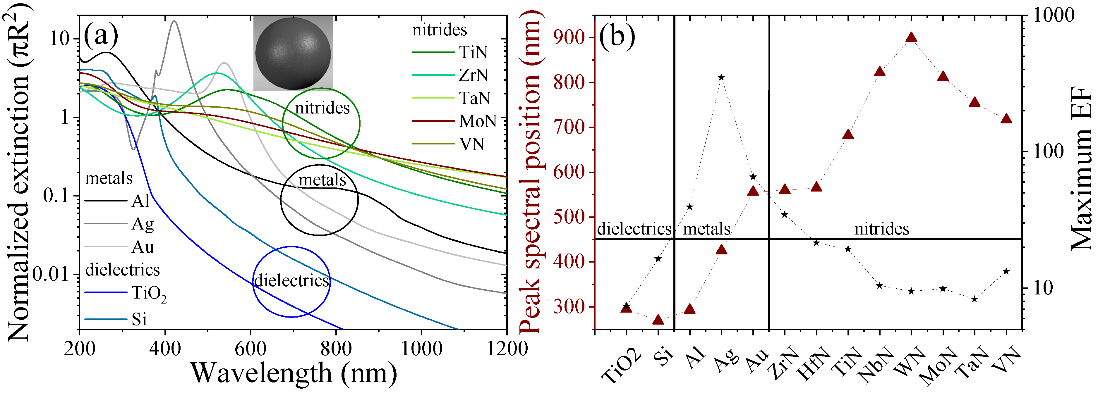
In a first step, we consider the optical properties of spherical nanoparticles using three different material classes. Figure 2a shows the Mie scattering and the maximum near-field enhancement at the particle surface at the resonance positions of the different materials is collected in Figure 2b. Metals continue to receive much attention for photonic applications because they show the strongest field enhancement factor (EF), note the logarithmic scale. In dye-sensitized solar cells or other systems relying on the field enhancement of added nanoparticles, metals remain a prime choice. On the other hand, the selected dielectrics and nitrides show a moderate field enhancement. There are few materials that are close to (TiN, HfN, Si, VN) or above (ZrN) the (arbitrary) line of separation at . Overall, nitrides show a similar or higher EF than the considered dielectrics. In addition, electrochemical growth of nitride nanopillars can lead to additional doping of the systems [51,52] and thus yield overall higher field enhancement factors comparable with metal systems.
The considered materials cover a broad range of resonance positions, see Figure 2b, and careful selection for specific applications beyond PV applications, e.g., the enhancement of a photoluminescence process, enables optimal results. The distinctive plasmonic peaks of metals are typically rather narrow and associated with high losses, reflected in the peaks of the corresponding extinction in Figure 2a. This graph reveals another potential problem of transition metal nitrides. Although their plasmonic peaks are not as strong as for typically employed metals and they improve solar cell performance at wavelengths where metals strongly absorb, their long wavelength absorption is stronger than for all the other materials investigated. This could already have been guessed from the imaginary part of the illustrated permittivities in Figure 1c. Compared to metals, photon absorption in the blue spectral regions can be improved with transition metal nitrides, but the absorption at larger wavelengths indicates that overall losses for solar applications might be accumulating too much. Thus, dielectric Mie resonators, in particular from Si, remain the most efficient light scatterers over a broad spectral range.
From this, particle clusters can be studied with multiple scattering techniques [33] with a particular interest in self-assembled and chemically synthesized layers where the particles are distributed randomly in a cluster [34]. The scattering matrix for nanoparticles of arbitrary shapes can be obtained with, e.g., BEM (Boundary Element Method), DDA (Discrete Dipole Approximation) or FEM (Finite Element Method) [30,32] allowing the study of a wealth of nanoparticle shapes in such additional layers.
The considered solar cell device, a complex nanostructured and layered system, is modeled with a scattering matrix approach employing the RCWA/FMM to a regular array of nanopillars as depicted in Figure 1b. For dielectric particles, this is a fast and reliable computational approach [4,53,54] that casts the electromagnetic wave equation into an eigenvalue problem via expansion in plane waves and Fourier transform of material parameters. This Fourier transform is analytical for cylindrical particle shapes (or, vice versa, holes) allowing for easy extensions towards multi-type particle distributions [4] or multi-walled systems such as nanotubes [51,55]. In these calculations, metal nanostructures pose limitations due to the high refractive index contrast with their environment. Transition metal nitrides show similar permittivity values as metals, see Figure 1c,d, and are, thus, facing the same challenges in plane-wave expansion approaches where many plane waves must be considered to arrive at a converged result, yielding longer computational times. In the next section, we introduce in detail the procedure to adiabatically include the measured doping profiles of n+– and p+–doped regions, see Figure 3a, into the central n–doped c-Si wafer.
2.1.1. Doped Baseline Solar Cell—Free Carrier Absorption in Doped Si
Light propagates in free space according to its wavenumber depending on its frequency or wavelength , resp., with velocity c. When propagating within a device, refraction and losses occur, effects which are captured in the frequency-dependent refractive index n of a medium, such that . The real and imaginary part of the permittivity of a material are related to the wavenumber through Maxwell’s equations, in particular , where is the constant permittivity of free space. This relates to the wavenumber
where the imaginary contribution gives the absorption coefficient . Finally, the real valued refractive index yields
This is typically approximated to for low absorptivity or even to a constant value where material parameters vary slowly in the spectral window of interest. Here, tabulated, i.e., frequency-dependent data [56] is used for the permittivity of Si without restricting to such approximations due to the large spectral region of interest for photovoltaic devices. Therefore, we obtain the absorption coefficient of Si from
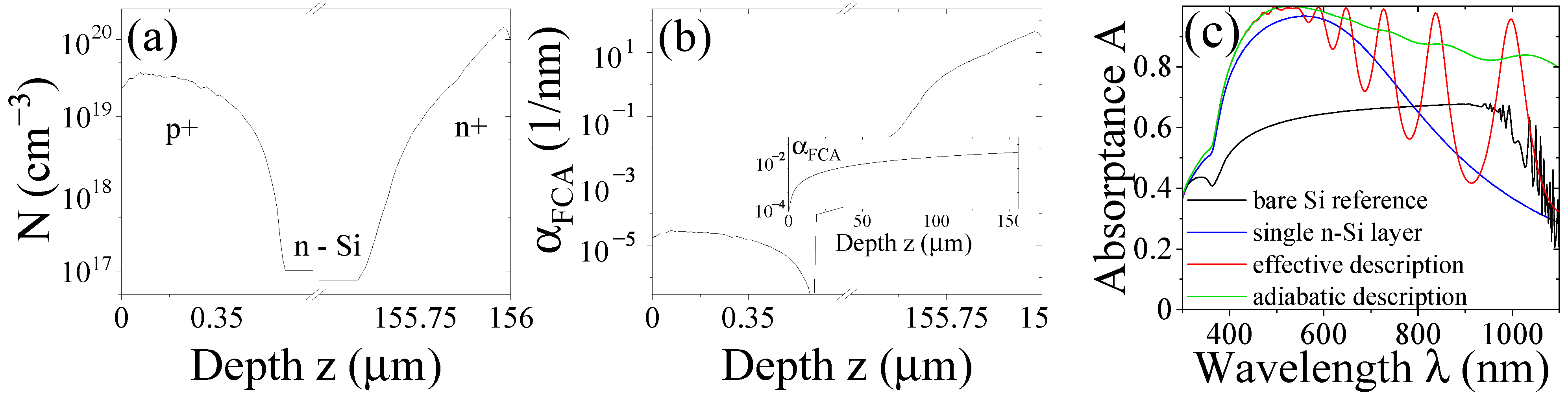
This coefficient is a measure of the exponential absorption inside the considered material with intensity dropping as . The inverse of Equation (3) can be used to reconstruct the related permittivity . With this approach the effect of free carrier absorption in highly doped Si is added to the experimentally available permittivity of undoped Si [56]. Using measured data for the electron density in c-Si wafers, we calculate the FCA and resulting modified permittivity following the empirical relation discussed in depth in Ref. [48]. Hereby, we use their results on p+–doping ( and ) and n+–doping ( and ). The range of validity is given for m} and due to available data in their study. The calculations presented here are within the VIS (visible) spectrum. Moreover, we use measured doping profiles to add this absorption effect to the optical simulations. This allows a realistic description of the baseline cell design. To evaluate the performance of solar cells, we integrate the calculated absorption over the visible spectrum to obtain the short circuit photocurrent
where q is the electric charge, h is the Planck constant, and is the solar spectrum. The total device absorption is directly related to the external quantum efficiency accounting for reflection losses and calculated with the aforementioned RCWA/FMM method as after evaluating the reflected and transmitted energy flux R and T, respectively. However, when considering particle arrays in the simulation, we can concentrate on the absorption occurring in the Si solar cell only , excluding parasitic absorption in the particle array and thus taking only scattering and field enhancement effects into account that impact the Si solar cell. Finally, the relative photocurrent gain is calculated from
comparing the photocurrent of the baseline cell with the one decorated with nanopillars.
2.1.2. Adding Nanoparticle Layers
The iterative scattering matrix approach for multilayered systems can cope with nanostructured layers within the RCWA/FMM and allows the integration of particle distributions based on the Fourier transform of a unit cell [53,54]. Here, cylindrical disks or nanopillars are used in a regular square lattice on top of the active c-Si layer within the SiN passivation layer. Then, for fixed geometrical parameters such as the disk height and distance, the solar device performance for different materials is compared. Typically, convergence is sufficiently fast for dielectric particle layers and complex particle distributions within the unit cell can be studied [4], while large contrasts in permittivity make convergence tedious for metals and transition metal nitrides where a higher number of diffracted light beams needs to be taken into account. The material data of nitrides has been gathered from a wide range of measurements in the reviews of Refs. [21,22,23] and is the basis for the calculations.
3. Results and Discussion
For each subdivision of the c-Si layer, the free carrier absorption is calculated and from this the modified permittivity of doped Si which results in capturing the absorption effects, see Figure 3b, beyond the usage of available data [56] for undoped bulk material. These multilayered systems typically converge for ∼ subdivisions. The total width of this c-Si region is m and the additional doping profiles affect about m at the front and back of the structure, respectively.
We study the impact of the FCA effect in Figure 3c. The absorption for a standalone, undoped Si layer is compared to an n–doped Si layer sandwiched between ultrathin SiN layers. This improves the absorption at short wavelengths to over 98% in the 500–550 nm region reaching 100% in a narrow spectral range as compared to a maximum of 97% in the case of an n–doped Si layer. The latter reaches an absorption above 90% between 450–650 nm while the former has an extended high absorption region between 425–770 nm. We used also a three-layer model with effective charge carrier densities for p+–, n–, and n+–doped layers derived from the measured doping profile as
integrating over the three regions depicted in Figure 3a. This shows Fabry-Pérot oscillations with large amplitudes, improving the absorption further only at specific wavelengths. Hence, using the adiabatic scheme of multilayers as outlined above, we obtain the optical response of the system to much accuracy which is also reflected in the calculated which is discussed next.
The outlined procedure is powerful because it allows the rapid investigation of several nanostructures on top of a highly accurate, highly optimized baseline cell made of hundreds of layers following the doping profile. The photocurrent for the baseline cell before introducing the front side emitter and back surface field is mA/cm. Adding the free carrier absorption through the doping profiles increases the photocurrent for the completed baseline cell to mA/cm. In comparison, the measured photocurrent for the n-PERT BiSoN cell including an antireflection coating is mA/cm. In the least, we expect the additional nanoparticle layer to boost the efficiency of the flat baseline cell to that of the finished industrial cell. In all the discussed cases, we are integrating over the spectral window of 300 to 1200 nm.
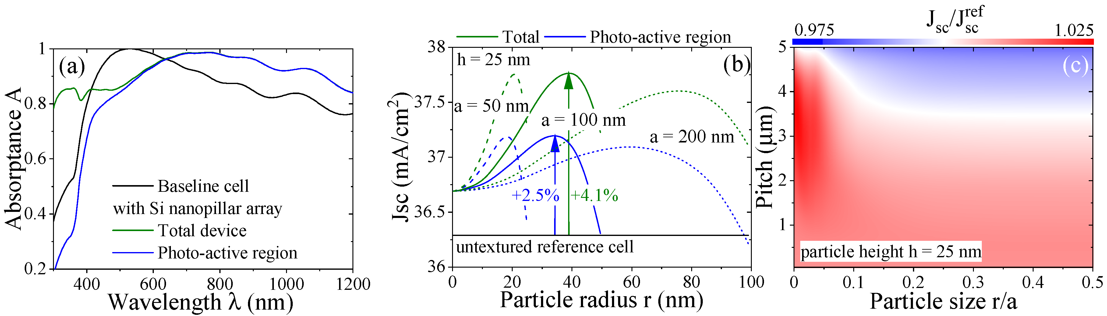
We compare in Figure 4a different device structures including the free carrier absorption effect of the measured doping profiles. The total width of the photo-active Si region is m. The absorption for the baseline cell without nanopillar array, an n–doped Si layer sandwiched between ultrathin SiN layers is compared to cases with added Si nanopillars placed within the SiN layer on top of the solar cell such that their height adds to the thickness of the front SiN layer. This improves the absorption at shorter and longer wavelengths while reducing the efficiency around the highly optimized region. However, we believe that calculating the total device absorption overestimates the benefits for the solar cell, as absorption occurring within the nanostructure itself cannot easily lead to the generation of carriers useful for the photovoltaic effect. Hence, we perform calculations of the portion of the absorption within the photo-active Si layer only, following its doping profile. The benefits of the nanostructure on top of this region stems then from scattering and near-field effects directly at the interface to the active Si layer. Excluding, thus, the parasitic absorption occurring in the nanoparticles and accounting for internal device absorption only, it can be seen that this benefit is at long wavelengths while light with short wavelengths is absorbed already in the particle layer and will in most cases not contribute to the photovoltaic effect.
In Figure 4b, the wavelength-independent short circuit current is shown as a function of particle size, nanopillar height fixed at nm, and three particle separations. Here, the absorption of the whole device (green curves) and the absorption of only the photo-active Si wafer (blue curves) are considered separately thus excluding parasitic absorption effects in the particle layer itself. Since the baseline cell is already highly optimized, the nanoparticle layer adds only a few percent to the photocurrent gain. For the different geometries, distinct optimum particle sizes are found. Although all cases show an increase in the photocurrent, the calculation considering the total absorptance in the system overestimates the benefits of employing nanoparticles. Finally, Figure 4c shows the dependence on the nanopillar radius size and distance for a fixed height for the case of excluding parasitic absorption in the nanostructure. The relative change in the photocurrent can be both positive or negative. For the range shown, dielectric Si nanopillars mostly enhance the photocurrent, though excluding absorption in the particle layer rarely results in a relative photocurrent gain above . In particular, the region for large particle separations at low size-to-distance ratios shows strong enhancement of the photocurrent. This is the condition for Black Silicon structures [57].
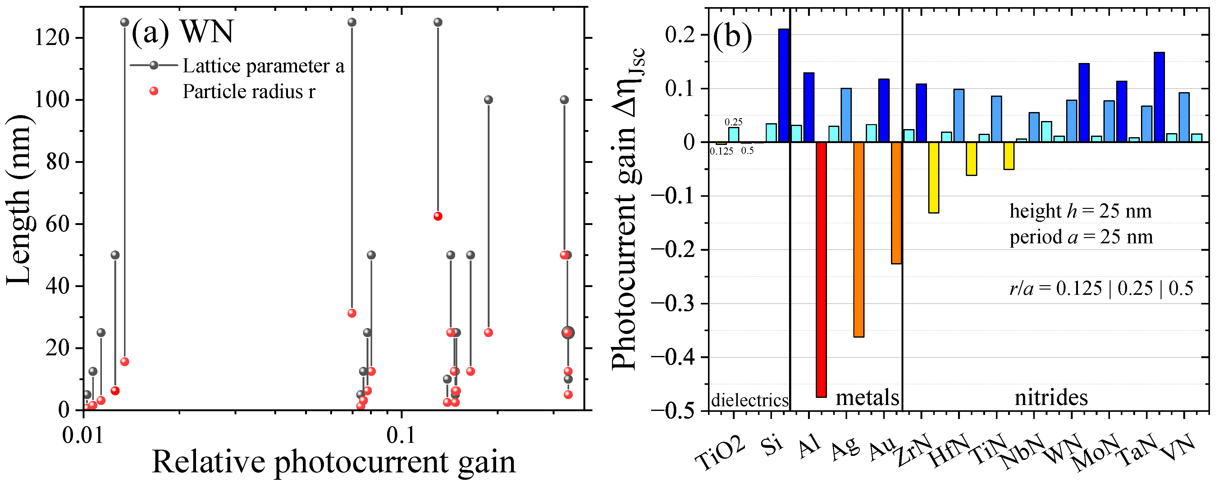
A similar analysis for nitride nanopillar arrays yields the results presented in Figure 5. For WN as a representative of this material class, Figure 5a shows the relative photocurrent gain for many combinations of nanopillar radius and distance (lattice parameter) yielding over 30% relative gain with respect to the untextured baseline cell in several cases. A competitive overview of results for is given in Figure 5b for three geometric sets of nanopillar layers with varying -ratio. To each material , , and are shown side-by-side. The colors are meant as a guide to the eye: yellow for moderate, orange or red for high losses often due to parasitic material absorption in the nanostructure itself. The different shades of blue indicate positive photocurrent gain from minor (light blue) to moderate (dim blue) to large (bright blue) gains. Metals show strong losses for the case of touching nanopillars (). The same is true for those nitrides whose plasmonic resonance is most comparable to gold, i.e., ZrN and HfN and, thus, have an overlap with the optimized spectral region of the baseline solar cell. In these cases, the absorption in the nanoparticle layer strongly hinders the absorption within the baseline cell. Overall, this case is connected to the shading effect. If too much additional material is placed on top of the solar cell device, the incident light will be either reflected or absorbed in the particle layer itself, which strongly reduces the photocurrent yield.
Typically, most materials have their largest photocurrent gain for the medium sized nanopillar structure, i.e., there is not too much nor too little scattering material. In contrast, some materials show strongest photocurrent gain for the largest particle to lattice parameter ratio. This includes the dielectric Si and the nitrides WN, MoN and TaN with relative gain of over 10% in these particular cases, which is one of the reasons to select WN for the more detailed analysis of Figure 5a. From all the nitrides studied, these materials look most promising combining the best of the two other worlds: their field enhancement is moderate and their associated plasmon resonance is far away from the wavelength region where the baseline cell is highly optimized, hence, contributing to improve the device at other wavelengths. At the same time, they exhibit strongest photocurrent gains for further increasing the nanopillar particle size.
4. Conclusions
We presented a comparative study of the relative photocurrent gain in solar cells employing nanopillar arrays made of three major material classes–dielectrics, metals and nitrides. The outlined numerical framework allows rapid and versatile modeling of realistic PV devices with arbitrary nanoparticle layers including the investigation of optimized doping profiles. This study is scalable and allows the inclusion of quantum correction schemes for metal nanoparticles or highly doped systems as outlined in the introduction. To simulate the baseline cell to much accuracy, we used doping profiles of an industry-level c-Si n-PERT solar cell to incorporate the effect of free carrier absorption into the optical simulations. With this, we yield a photocurrent of mA/cm in comparison to our simulated baseline cell without the FCA of mA/cm. The measured photocurrent for the n-PERT BiSoN cell including an antireflection coating is = mA/cm. The effect of FCA is, thus, very important for a realistic description of the solar cell device.
The configurations studied here readily show an increase in the short circuit current for all materials studied to a degree, where they reach or go beyond the short circuit current of the finished industrial device including an antireflection coating, but no nanoparticles. Excluding absorption in the particle layer for Si nanopillars typically results in a relative photocurrent gain above . Considering a c-Si baseline structure, this could be a setup where absorption in the nanostructure does not have to be considered parasitic, as there is no chemical (leading to carrier diffusion) or mechanical (leading to strain) difference between the layers.
However, employing nanostructures at too low or too high coverage reduces beneficial absorption in most setups. In particular, metals show a strong shading effect, absorbing themselves or backscattering the incident light strongly if the surface coverage becomes too large. Transition metal nitrides can exhibit the same problem, especially when their own plasmon-type resonance is around the band gap or at its double frequency of the photo-active region (Si in this study), but overall the shading effect is strongly reduced compared to metals. On the bright side, some nitrides were identified with moderate field enhancement and highest photocurrent gain for largest nanopillar radius-to-distance ratios, i.e., no shading effect. These materials show low absorption and mostly favorable forward scattering similar to the commonly used dielectric materials. Black silicon could, hence, be substituted by Black nitrides such as WN, MoN and TaN. For the case of WN studied to much detail here, some combinations of nanopillar radius and distance were found yielding over 30% relative gain with respect to the untextured baseline cell. On average a relative gain of over 10% in these particular cases was found.
Author Contributions
Data curation, C.D. and L.J.K.; Formal analysis, C.D.; Investigation, C.D. and L.J.K.; Methodology, C.D.; Software, C.D.; Validation, C.D.; Visualization, L.J.K.; Writing—original draft, C.D.; Writing—review & editing, L.J.K. and R.K. All authors have read and agreed to the published version of the manuscript.
Funding
The APC was funded by the Thüringer Universitäts- und Landesbibliothek Jena (ThULB).
Data Availability Statement
The datasets generated and analyzed during the presented study are available upon reasonable request from the corresponding author.
Conflicts of Interest
The authors declare no conflict of interest.
References
- Catchpole, K.R.; Polman, A. Plasmonic solar cells. Opt. Express 2008, 16, 21793–21800. [Google Scholar] [CrossRef] [PubMed] [Green Version]
- Catchpole, K.R.; Polman, A. Design principles for particle plasmon enhanced solar cells. Appl. Phys. Lett. 2008, 93, 191113. [Google Scholar] [CrossRef] [Green Version]
- Tavkhelidze, A.; Bibilashvili, A.; Jangidze, L.; Gorji, N.E. Fermi-Level Tuning of G-Doped Layers. Nanomaterials 2021, 11, 505. [Google Scholar] [CrossRef] [PubMed]
- David, C. Multi-type particle layer improved light trapping for photovoltaic applications. Appl. Opt. 2016, 55, 7980–7986. [Google Scholar] [CrossRef] [PubMed] [Green Version]
- Atwater, H.A.; Polman, A. Plasmonics for improved photovoltaic devices. Nat. Mater. 2010, 9, 205–213. [Google Scholar] [CrossRef] [PubMed]
- Wang, E.; White, T.P.; Catchpole, K.R. Resonant enhancement of dielectric and metal nanoparticle arrays for light trapping in solar cells. Opt. Express 2012, 20, 13226–13237. [Google Scholar] [CrossRef]
- Mokkapati, S.; Beck, F.J.; de Waele, R.; Polman, A.; Catchpole, K.R. Resonant nano-antennas for light trapping in plasmonic solar cells. J. Phys. D Appl. Phys. 2011, 44, 185101. [Google Scholar] [CrossRef]
- Pillai, S.; Beck, F.J.; Catchpole, K.R.; Ouyang, Z.; Green, M.A. The effect of dielectric spacer thickness on surface plasmon enhanced solar cells for front and rear side depositions. J. Appl. Phys. 2011, 109, 073105. [Google Scholar] [CrossRef]
- Basch, A.; Beck, F.J.; Söderström, T.; Varlamov, S.; Catchpole, K.R. Combined plasmonic and dielectric rear reflectors for enhanced photocurrent in solar cells. Appl. Phys. Lett. 2012, 100, 243903. [Google Scholar] [CrossRef]
- Yan, W.; Stokes, N.; Jia, B.; Gu, M. Enhanced light trapping in the silicon substrate with plasmonic Ag nanocones. Opt. Lett. 2013, 38, 395–397. [Google Scholar] [CrossRef]
- Cortés-Juan, F.; Chaverri Ramos, C.; Connolly, J.P.; David, C.; García de Abajo, F.J.; Hurtado, J.; Mihailetchi, V.D.; Ponce-Alcántara, S.; Sánchez, G. Effect of Ag nanoparticles integrated within antireflection coatings for solar cells. J. Renew. Sustain. Energy 2013, 5, 033116. [Google Scholar] [CrossRef]
- Nozik, A.J. Multiple exciton generation in semiconductor quantum dots. Chem. Phys. Lett. 2008, 457, 3–11. [Google Scholar] [CrossRef]
- Barugkin, C.; Allen, T.; Chong, T.K.; White, T.P.; Weber, K.J.; Catchpole, K.R. Light trapping efficiency comparison of Si solar cell textures using spectral photoluminescence. Opt. Express 2015, 23, A391–A400. [Google Scholar] [CrossRef] [Green Version]
- Barugkin, C.; Wan, Y.; Macdonald, D.; Catchpole, K.R. Evaluating plasmonic light trapping with photoluminescence. IEEE J. Photovolt. 2013, 3, 1292–1297. [Google Scholar] [CrossRef]
- Mertens, H.; Biteen, J.S.; Atwater, H.A.; Polman, A. Polarization-Selective Plasmon-Enhanced Silicon Quantum-Dot Luminescence. Nano Lett. 2006, 6, 2622–2625. [Google Scholar] [CrossRef]
- Yeshchenko, O.A.; Dmitruk, I.M.; Alexeenko, A.A.; Losytskyy, M.Y.; Kotko, A.V.; Pinchuk, A.O. Size-dependent surface-plasmonenhanced photoluminescence from silver nanoparticles embedded in silica. Phys. Rev. B 2009, 79, 235438. [Google Scholar] [CrossRef]
- Yuan, Z.; Pucker, G.; Marconi, A.; Sgrignuoli, F.; Anopchenko, A.; Jestin, Y.; Ferrario, L.; Bellutti, P.; Pavesi, L. Silicon nanocrystals as a photoluminescence down shifter for solar cells. Sol. Energy Mater. Sol. Cells 2011, 95, 1224–1227. [Google Scholar] [CrossRef] [Green Version]
- Zhang, J.; Noguez, C. Plasmonic Optical Properties and Applications of Metal Nanostructures. Plasmonics 2008, 3, 127–150. [Google Scholar] [CrossRef]
- Beck, F.J.; Mokkapati, S.; Catchpole, K.R. Light trapping with plasmonic particles: Beyond the dipole model. Opt. Express 2011, 19, 25230–25241. [Google Scholar] [CrossRef] [PubMed]
- Albella, P.; García-Cueto, B.; González, F.; Moreno, F.; Wu, P.C.; Kim, T.H.; Brown, A.; Yang, Y.; Everitt, H.O.; Videen, G. Shape Matters: Plasmonic Nanoparticle Shape Enhances Interaction with Dielectric Substrate. Nano Lett. 2011, 11, 3531–3537. [Google Scholar] [CrossRef] [PubMed] [Green Version]
- Metaxa, C.; Kassavetis, S.; Pierson, J.; Gall, D.; Patsalas, P. Infrared Plasmonics with Conductive Ternary Nitrides. ACS Appl. Mater. Interfaces 2017, 9, 10825–10834. [Google Scholar] [CrossRef] [PubMed]
- Patsalas, P.; Kalfagiannis, N.; Kassavetis, S. Optical Properties and Plasmonic Performance of Titanium Nitride. Materials 2015, 8, 3128. [Google Scholar] [CrossRef] [Green Version]
- Patsalas, P.; Kalfagiannis, N.; Kassavetis, S.; Abadias, G.; Bellas, D.; Lekka, C.; Lidorikis, E. Conductive nitrides: Growth principles, optical and electronic properties, and their perspectives in photonics and plasmonics. Mater. Sci. Eng. R Rep. 2018, 123, 1–55. [Google Scholar] [CrossRef]
- Milanova, M.; Donchev, V.; Kostov, K.L.; Alonso-Álvarez, D.; Terziyska, P.; Avdeev, G.; Valcheva, E.; Kirilov, K.; Georgiev, S. Study of GaAsSb:N bulk layers grown by liquid phase epitaxy for solar cells applications. Mater. Res. Express 2019, 6, 075521. [Google Scholar] [CrossRef]
- Green, M.; Dunlop, E.; Hohl-Ebinger, J.; Yoshita, M.; Kopidakis, N.; Hao, X. Solar cell efficiency tables (version 57). Prog. Photovolt. Res. Appl. 2020, 29, 3–15. [Google Scholar] [CrossRef]
- Hamed, T.A.; Adamovic, N.; Aeberhard, U.; Alonso-Alvarez, D.; Amin-Akhlaghi, Z.; Der Maur, M.A.; Beattie, N.; Bednar, N.; Berland, K.; Birner, S.; et al. Multiscale in modelling and validation for solar photovoltaics. EPJ Photovolt. 2018, 9, 10. [Google Scholar] [CrossRef]
- Raza, S.; Bozhevolnyi, S.I.; Wubs, M.; Mortensen, N.A. Nonlocal optical response in metallic nanostructures. J. Phys. Cond. Matter. 2015, 27, 183204. [Google Scholar] [CrossRef] [Green Version]
- Krasavin Alexey, V.; Pavel, G.; Zayats Anatoly, V. Free-electron Optical Nonlinearities in Plasmonic Nanostructures: A Review of the Hydrodynamic Description. Laser Photonics Rev. 2018, 12, 1700082. [Google Scholar] [CrossRef] [Green Version]
- Mie, G. Beiträge zur Optik trüber Medien, speziell kolloidaler Metallösungen. Ann. Phys. 1908, 330, 377–445. [Google Scholar] [CrossRef]
- Myroshnychenko, V.; Rodríguez-Fernández, J.; Pastoriza-Santos, I.; Funston, A.M.; Novo, C.; Mulvaney, P.; Liz-Marzán, L.M.; de Abajo, F.J.G. Modelling the optical response of gold nanoparticles. Chem. Soc. Rev. 2008, 37, 1792–1805. [Google Scholar] [CrossRef] [Green Version]
- Alvarez-Puebla, R.; Liz-Marzán, L.M.; García de Abajo, F.J. Light Concentration at the Nanometer Scale. J. Phys. Chem. Lett. 2010, 1, 2428–2434. [Google Scholar] [CrossRef]
- de Abajo, F.J.G. Colloquium: Light scattering by particle and hole arrays. Rev. Mod. Phys. 2007, 79, 1267–1290. [Google Scholar] [CrossRef] [Green Version]
- de Abajo, F.J.G. Multiple scattering of radiation in clusters of dielectrics. Phys. Rev. B 1999, 60, 6086–6102. [Google Scholar] [CrossRef]
- David, C.; Connolly, J.P.; Chaverri Ramos, C.; García de Abajo, F.J.; Sánchez Plaza, G. Theory of random nanoparticle layers in photovoltaic devices applied to self-aggregated metal samples. Sol. Energy Mater. Sol. Cells 2013, 109, 294–299. [Google Scholar] [CrossRef] [Green Version]
- David, C.; Christensen, J.; Mortensen, N.A. Spatial dispersion in two-dimensional plasmonic crystals: Large blueshifts promoted by diffraction anomalies. Phys. Rev. B 2016, 94, 165410. [Google Scholar] [CrossRef] [Green Version]
- Dehghani, M.; David, C. Light Scattering from Rough Silver Surfaces: Modeling of Absorption Loss Measurements. Nanomaterials 2021, 11, 113. [Google Scholar] [CrossRef] [PubMed]
- Jäger, K.; Fischer, M.; van Swaaij, R.A.C.M.M.; Zeman, M. A scattering model for nano-textured interfaces and its application in opto-electrical simulations of thin-film silicon solar cells. J. Appl. Phys. 2012, 111, 083108. [Google Scholar] [CrossRef]
- Joannopoulos, J.D.; Johnson, S.G.; Winn, J.N.; Meade, R.D. Photonic Crystals: Molding the Flow of Light, 2nd ed.; Princeton University Press: Princeton, NJ, USA, 2008. [Google Scholar]
- David, C.; García de Abajo, F.J. Spatial Nonlocality in the Optical Response of Metal Nanoparticles. J. Phys. Chem. C 2011, 115, 19470–19475. [Google Scholar] [CrossRef]
- David, C.; Mortensen, N.A.; Christensen, J. Perfect imaging, epsilon-near zero phenomena and waveguiding in the scope of nonlocal effects. Sci. Rep. 2013, 3, 2526. [Google Scholar] [CrossRef] [PubMed] [Green Version]
- Jacak, W.A. Propagation of Collective Surface Plasmons in Linear Periodic Ionic Structures: Plasmon Polariton Mechanism of Saltatory Conduction in Axons. J. Phys. Chem. C 2015, 119, 10015–10030. [Google Scholar] [CrossRef]
- David, C.; Christensen, J. Extraordinary optical transmission through nonlocal holey metal films. Appl. Phys. Lett. 2017, 110, 261110. [Google Scholar] [CrossRef] [Green Version]
- Kluczyk, K.; Jacak, L.; Jacak, W.; David, C. Microscopic Electron Dynamics in Metal Nanoparticles for Photovoltaic Systems. Materials 2018, 11, 1077. [Google Scholar] [CrossRef] [Green Version]
- Kluczyk-Korch, K.; Jacak, L.; Jacak, W.A.; David, C. Mode Splitting Induced by Mesoscopic Electron Dynamics in Strongly Coupled Metal Nanoparticles on Dielectric Substrates. Nanomaterials 2019, 9, 1206. [Google Scholar] [CrossRef] [PubMed] [Green Version]
- Kluczyk, K.; David, C.; Jacak, J.; Jacak, W. On Modeling of Plasmon-Induced Enhancement of the Efficiency of Solar Cells Modified by Metallic Nano-Particles. Nanomaterials 2019, 9, 3. [Google Scholar] [CrossRef] [PubMed] [Green Version]
- Mihailetchi, V.D.; Jourdan, J.; Edler, A.; Kopecek, R.; Harney, R.; Stichtenoth, D.; Lossen, J.; Böscke, T.S.; Krokoszinski, H.-J. Screen printed n-type silicon solar cells for industrial application. In Proceedings of the 25th European Photovoltaic Solar Energy Conference and Exhibition, Valencia, Spain, 6–9 September 2010; pp. 6–10. [Google Scholar]
- Edler, A. Development of Bifacial n-Type Solar Cells for Industrial Application. PhD Thesis, Libraray of the University of Konstanz, Konstanz, Germany, 2014. [Google Scholar]
- Baker-Finch, S.C.; McIntosh, K.R.; Yan, D.; Fong, K.C.; Kho, T.C. Near-infrared free carrier absorption in heavily doped silicon. J. Appl. Phys. 2014, 116. [Google Scholar] [CrossRef] [Green Version]
- Rodrigo, S.G.; García-Vidal, F.J.; Martín-Moreno, L. Influence of material properties on extraordinary optical transmission through hole arrays. Phys. Rev. B 2008, 77, 075401. [Google Scholar] [CrossRef] [Green Version]
- Van Bui, H.; Kovalgin, A.Y.; Wolters, R.A.M. On the difference between optically and electrically determined resistivity of ultra-thin titanium nitride films. Appl. Surf. Sci. 2013, 269, 45–49. [Google Scholar] [CrossRef]
- Öner, I.H.; Querebillo, C.J.; David, C.; Gernert, U.; Walter, C.; Driess, M.; Leimkühler, S.; Ly, K.H.; Weidinger, I.M. High Electromagnetic Field Enhancement of TiO2 Nanotube Electrodes. Angew. Chem. Int. Ed. 2018, 57, 7225–7229. [Google Scholar] [CrossRef]
- David, C. Two-fluid, hydrodynamic model for spherical electrolyte systems. Sci. Rep. 2018, 8, 7544. [Google Scholar] [CrossRef]
- Whittaker, D.M.; Culshaw, I.S. Scattering-matrix treatment of patterned multilayer photonic structures. Phys. Rev. B 1999, 60, 2610–2618. [Google Scholar] [CrossRef] [Green Version]
- Liu, V.; Fan, S. S4: A free electromagnetic solver for layered periodic structures. Comput. Phys. Commun. 2012, 183, 2233–2244. [Google Scholar] [CrossRef]
- David, C. TiO2 Self-Assembled, Thin-Walled Nanotube Arrays for Photonic Applications. Materials 2019, 12, 1332. [Google Scholar] [CrossRef] [PubMed] [Green Version]
- Aspnes, D.E.; Studna, A.A. Dielectric functions and optical parameters of Si, Ge, GaP, GaAs, GaSb, InP, InAs, and InSb from 1.5 to 6.0 eV. Phys. Rev. B 1983, 27, 985–1009. [Google Scholar] [CrossRef]
- Liu, X.; Coxon, P.R.; Peters, M.; Hoex, B.; Cole, J.M.; Fray, D.J. Black silicon: Fabrication methods, properties and solar energy applications. Energy Environ. Sci. 2014, 7, 3223–3263. [Google Scholar] [CrossRef] [Green Version]
Figure 1.
Illustration of the considered setup and its range. (a) n-PERT BiSoN cell, here with flat passivating layer as simulated. (b) Cylindrical pillars of height d and radius R made of nitrides and other materials for comparison standing on the n-PERT device with particle-particle separation a. The nanopillars are placed within the SiN. Range of measured (c) real and (d) imaginary part of the permittivity of gold (orange [49]), TiN (blue [50]) and further nitride materials (grey [23]).
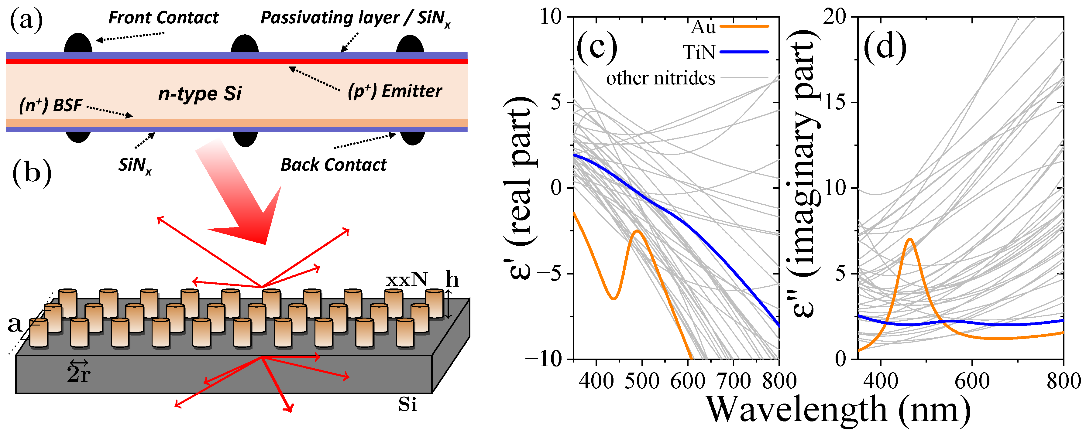
Figure 2.
Potential enhancement of absorption and local fields of various material classes. For spherical nanoparticles of radius nm of the depicted materials placed in a SiN host matrix the (a) normalized extinction and (b) maximum field enhancement factor (EF) and its the spectral position are given. The vertical lines separate the different material classes. The horizontal line lies at EF = 30.

Figure 3.
Si doping profiles as input for device modeling. (a) Electron doping as a function of the depth of the cell obtained from experimental measurements. (b) Calculated free carrier absorption across the cell. The inset shows the adiabatic connection in the n-doped center of width 150 m. (c) Comparing the achieved absorption using an intrinsic, an n-doped Si layer, an effective three-layer approach using average doping levels in front, back, and central region and an adiabatic approach using the full doping profile with effectively hundreds of layers in the scattering matrix scheme.

Figure 4.
Combined effects of a nanoparticle layer and free carrier absorption with and without parasitic absorption. (a) Absorption spectra for the baseline cell, with a Si nanopillar array and partial absorption only within the photo-active region. (b) The wavelength-independent short circuit current as a function of nanodisk radius showing results for both the total device absorption (green) and excluding absorption in the nanoparticles (blue). The untextured baseline cell is given as a reference. (c) Contour of the for a range of lattice parameters and particle sizes excluding parasitic absorption.

Figure 5.
Relative photocurrent gain for an n-doped Si solar cell with particle layers of different materials. (a) For WN as a representative of the class of nitrides, the relative photocurrent gain is given for a range of geometrical parameters. The data pairs show the lattice parameter a together with the radius r of the WN disks at heights and nm. (b) Comparing the different material classes for three geometrical setups with varying -ratio showing , , and side-by-side for each material.
Publisher’s Note: MDPI stays neutral with regard to jurisdictional claims in published maps and institutional affiliations. |
© 2021 by the authors. Licensee MDPI, Basel, Switzerland. This article is an open access article distributed under the terms and conditions of the Creative Commons Attribution (CC BY) license (https://creativecommons.org/licenses/by/4.0/).
Share and Cite
MDPI and ACS Style
David, C.; Koduvelikulathu, L.J.; Kopecek, R. Comparative Simulations of Conductive Nitrides as Alternative Plasmonic Nanostructures for Solar Cells. Energies 2021, 14, 4236. https://doi.org/10.3390/en14144236
AMA Style
David C, Koduvelikulathu LJ, Kopecek R. Comparative Simulations of Conductive Nitrides as Alternative Plasmonic Nanostructures for Solar Cells. Energies. 2021; 14(14):4236. https://doi.org/10.3390/en14144236
Chicago/Turabian StyleDavid, Christin, Lejo Joseph Koduvelikulathu, and Radovan Kopecek. 2021. "Comparative Simulations of Conductive Nitrides as Alternative Plasmonic Nanostructures for Solar Cells" Energies 14, no. 14: 4236. https://doi.org/10.3390/en14144236
Note that from the first issue of 2016, this journal uses article numbers instead of page numbers. See further details here.