
A Comprehensive Loss Model and Comparison of AC and DC Boost Converters

 , , , and
Abstract
1. Introduction and Motivation
1.1. AC and DC Converters
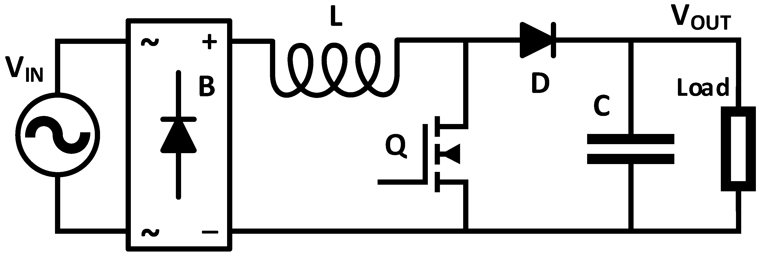
1.2. Boost Converters
2. Deriving Conduction Loss Models
3. Conduction Loss Component Currents
3.1. Input and Duty Cycle
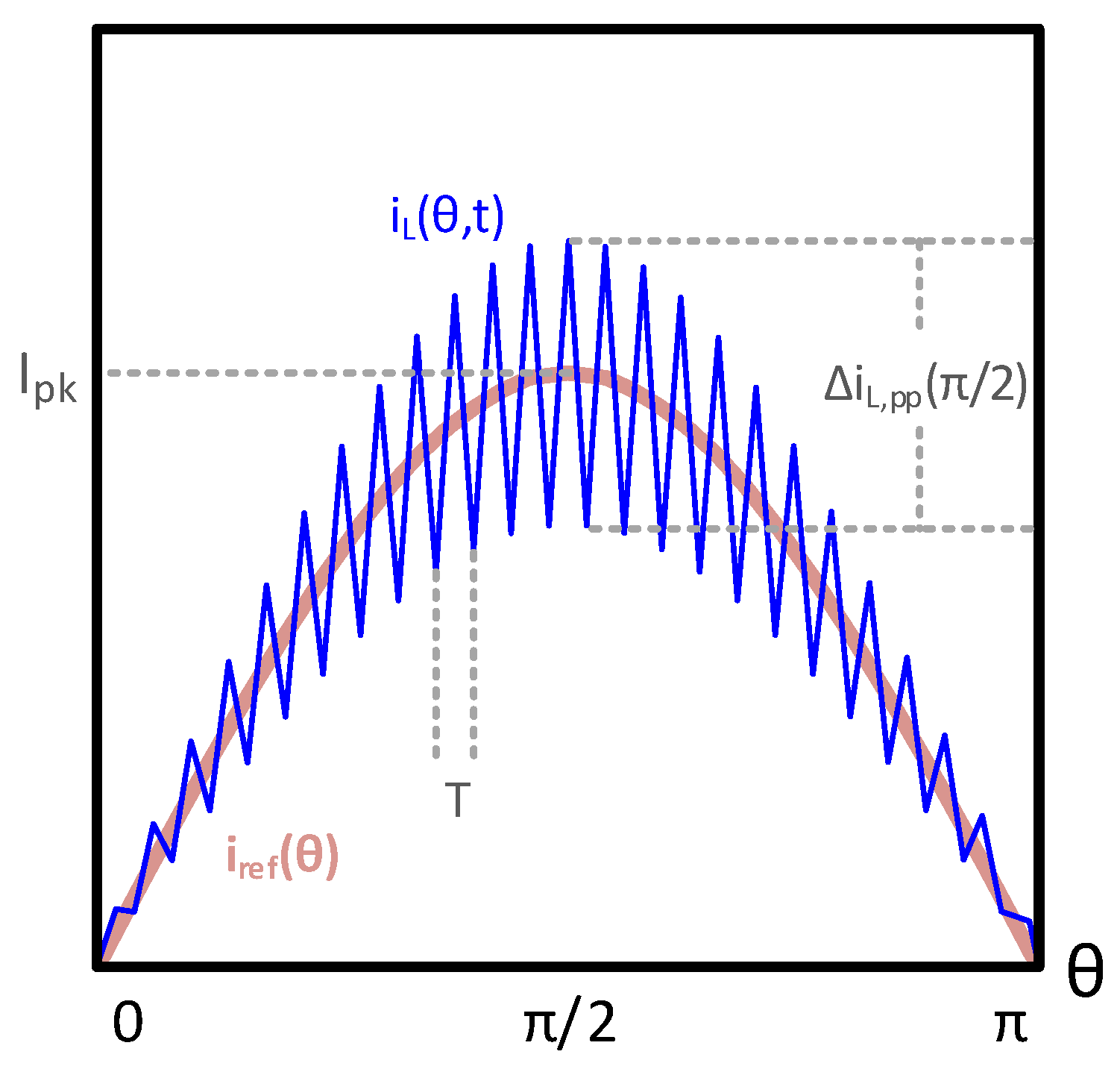
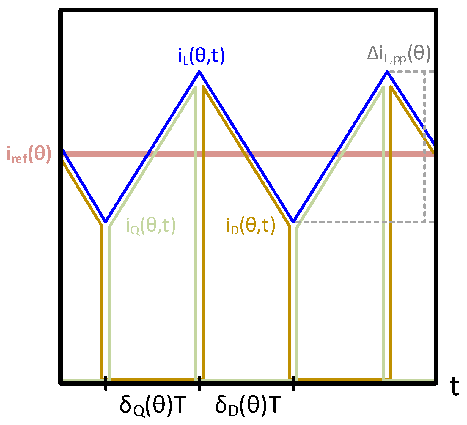
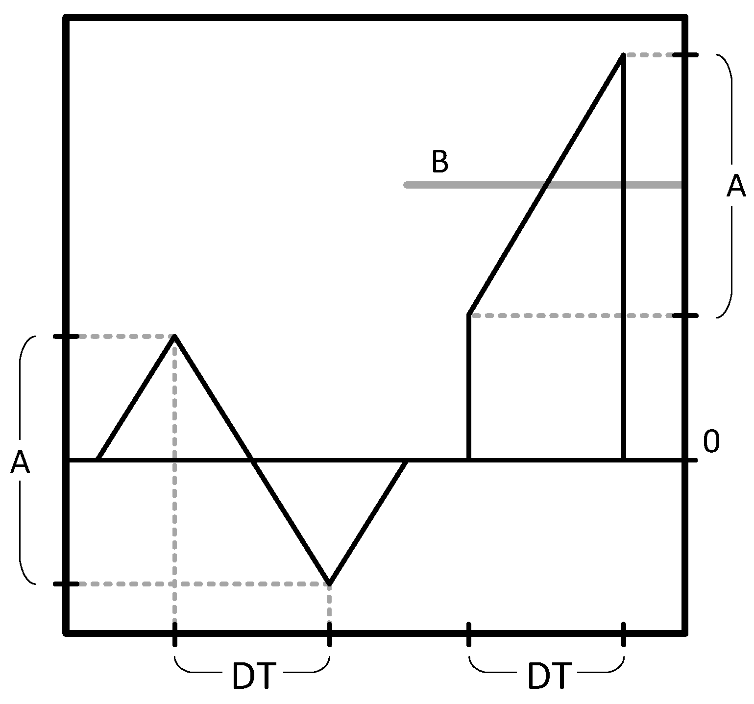
3.2. Inductor Current
3.3. Diode Bridge Current
3.4. Switch Current
3.5. Boost Diode Current
3.6. Capacitor Current
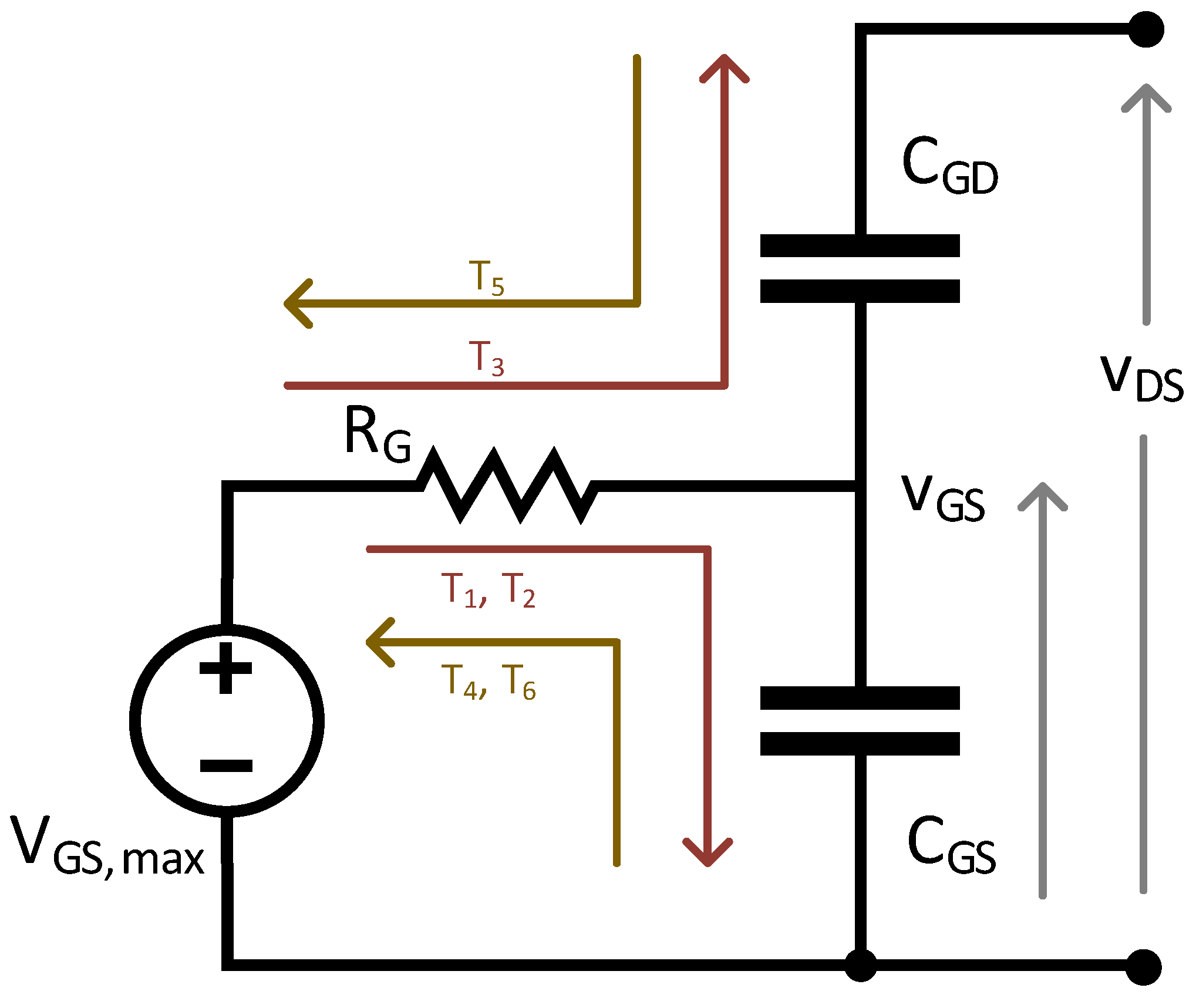
4. Switching Loss in the Switch (Q)
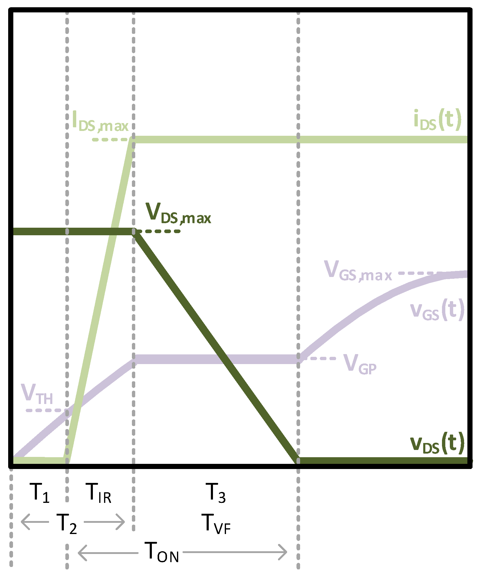
4.1. Hard-Switching Loss
- The gate driver charges . The gate voltage, , increases to the gate-threshold voltage, .
- The gate driver continues to charge . continues to increase as rises to .
- The gate driver now discharges . remains constant at the gate-plateau voltage, , as falls to near-zero.
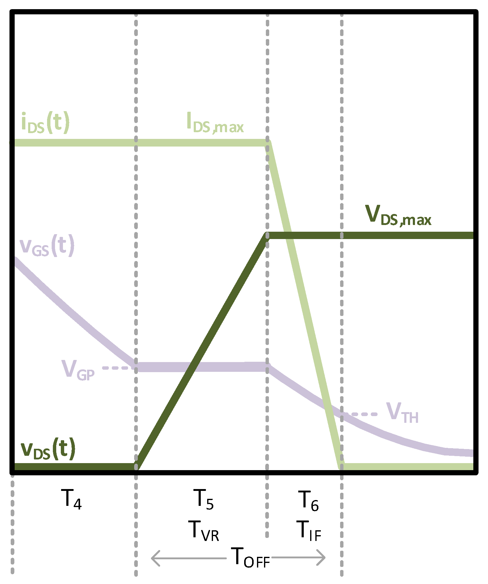
- 4.
- The gate driver discharges . decreases to .
- 5.
- The gate driver charges . remains constant at as rises to .
- 6.
- The gate driver discharges . decreases to and falls to near-zero.
4.2. Output-Capacitance Loss
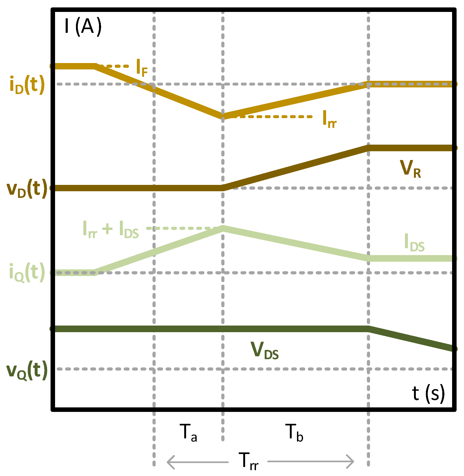
5. Switching Loss in the Diode (D)
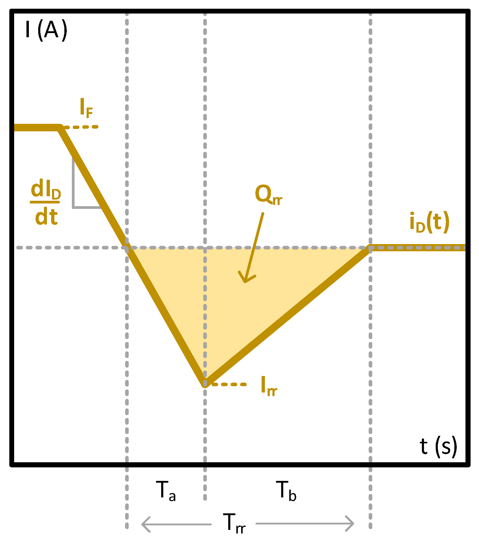
5.1. Reverse Recovery Loss
5.2. Junction-Capacitance Loss
6. Model Validation
6.1. Simulation Validation
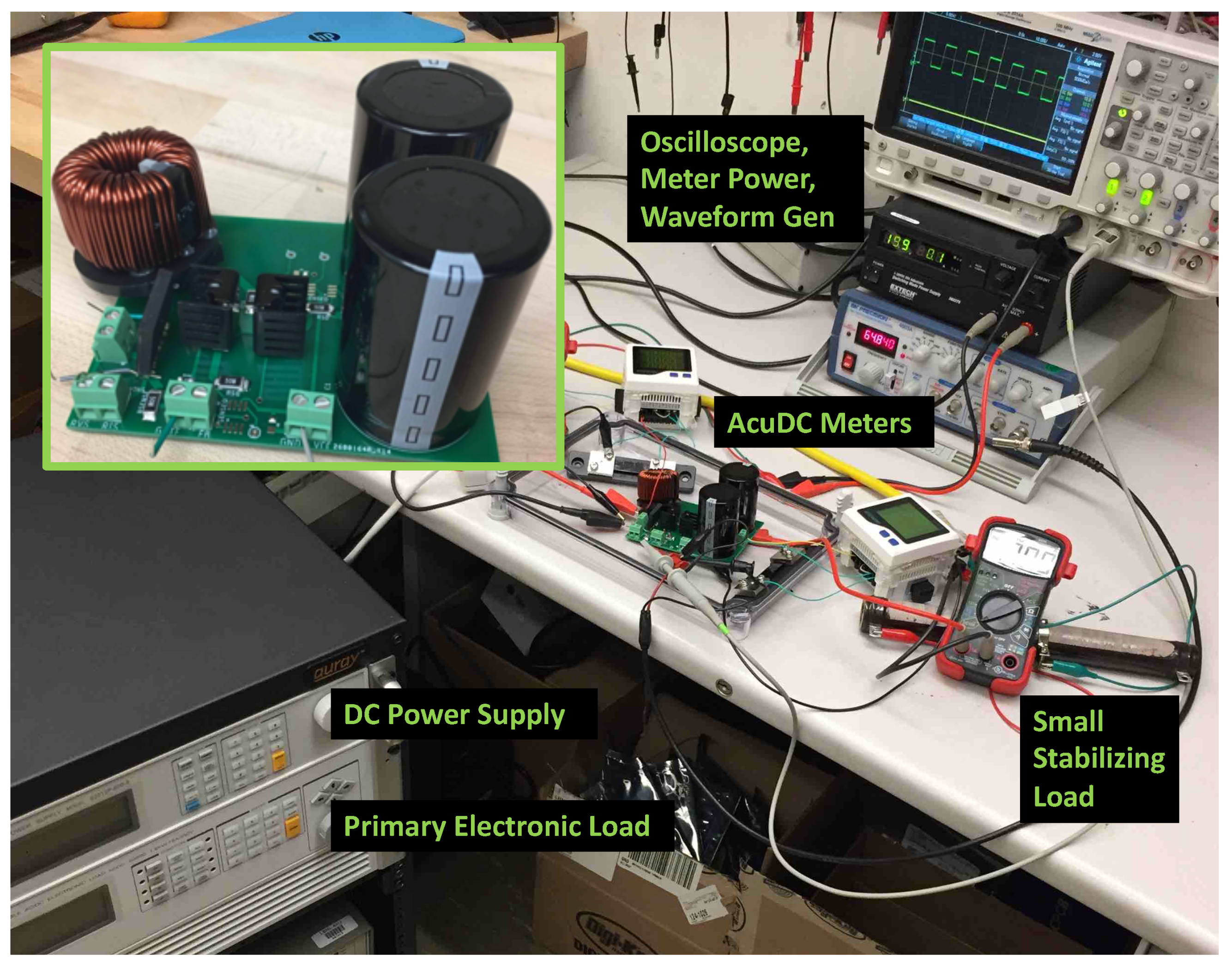
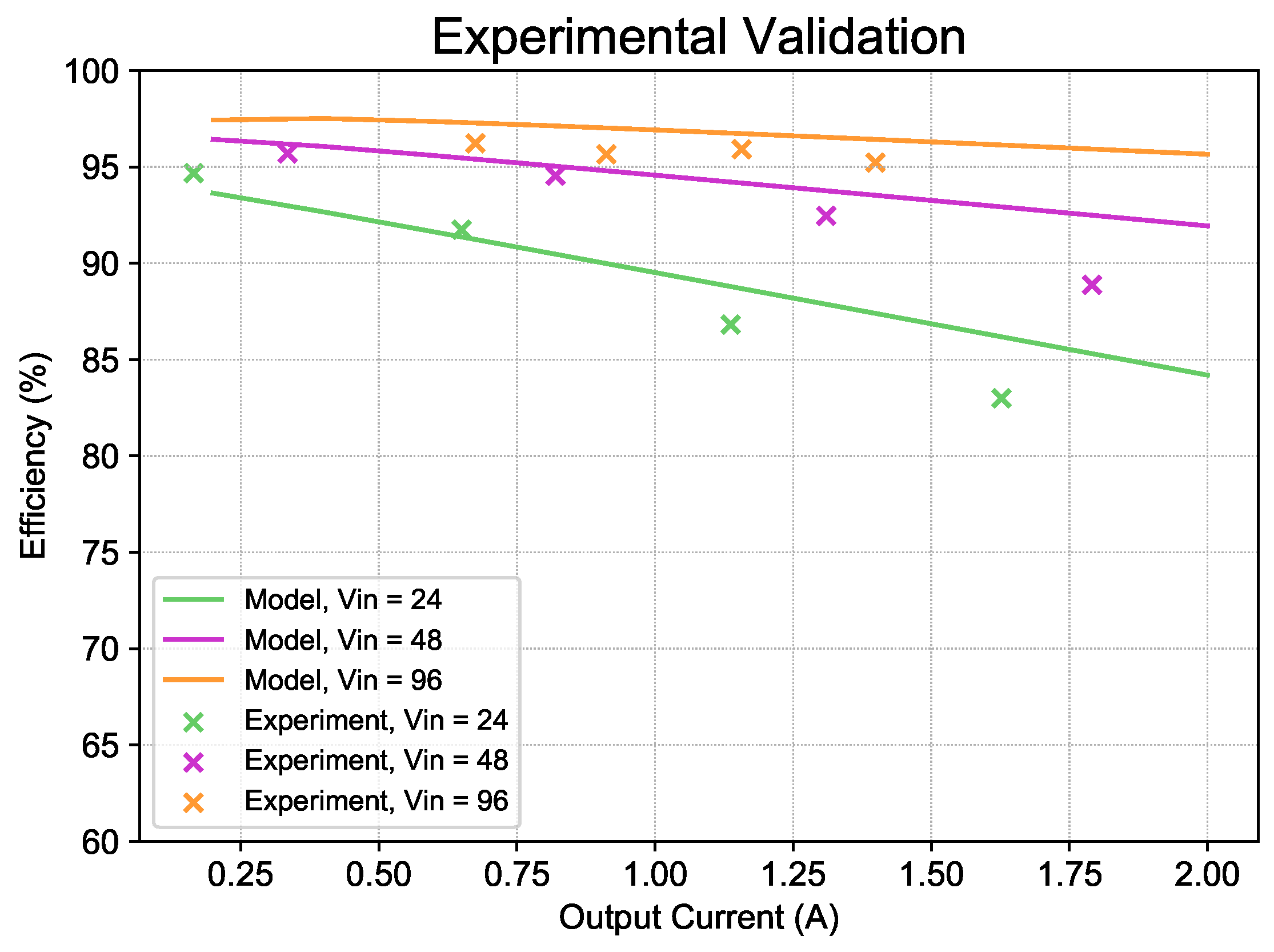
6.2. Experimental Validation
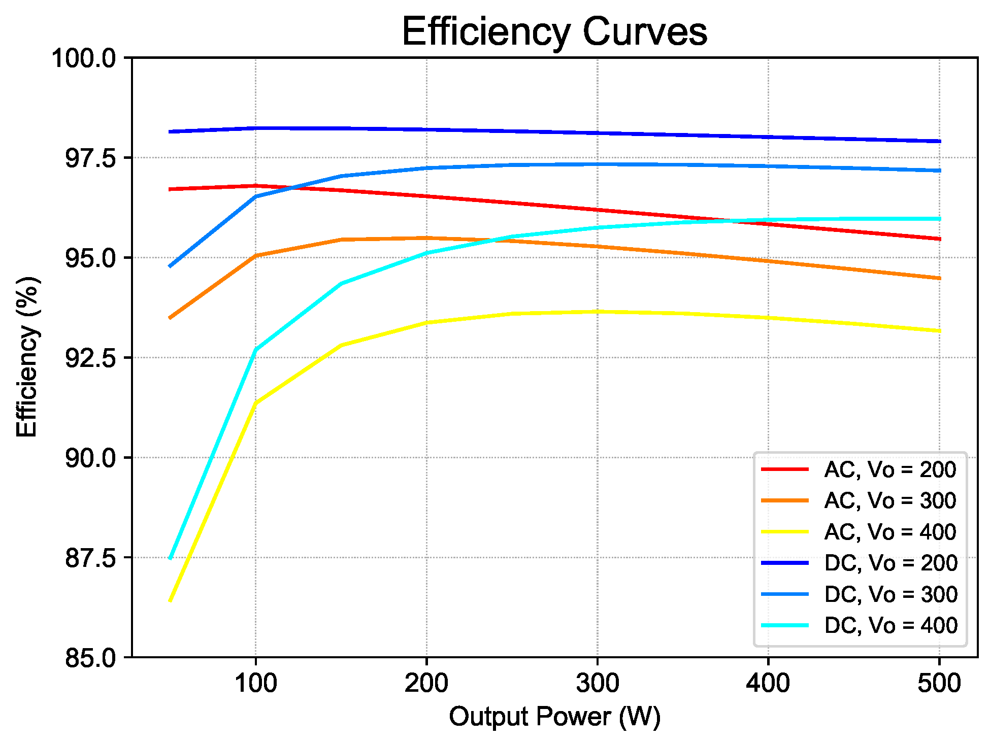
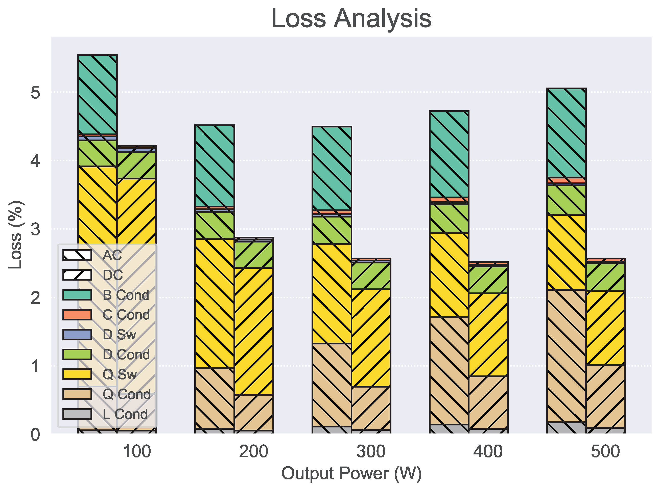
7. Efficiency Comparison of AC vs. DC
8. Conclusions and Future Work
Author Contributions
Funding
Institutional Review Board Statement
Informed Consent Statement
Data Availability Statement
Acknowledgments
Conflicts of Interest
Appendix A
Appendix A.1. Model Equations
Appendix A.2. PX,cond: Conduction Loss

| Parameter | AC PFC Model Formula | DC Model Formula |
|---|---|---|
| − | ||
| Parameter | Model Formula |
|---|---|
| − | |
| Parameter | Model Formula |
|---|---|
| − | |
| Parameter | Model Formula |
|---|---|
Appendix A.3. PQ,sw,hs and PQ,sw,c: Hard Switching and Output Capacitance Loss
| Timing | Formula |
|---|---|
| Model | Average Loss Power |
|---|---|
| AC PFC (simple) | |
| DC (simple) | |
| AC PFC (ripple) | |
| DC (ripple) |
Appendix A.4. PD,sw,hs and PD,sw,c: Diode Reverse Recovery and Junction Capacitance Loss
| Model | Average Loss Power |
|---|---|
| AC PFC (simple) | |
| DC (simple) | |
| AC PFC (ripple) | |
| DC (ripple) |
References
- Backhaus, S.; Swift, G.W.; Chatzivasileiadis, S.; Tschudi, W.; Glover, S.; Starke, M.; Wang, J.; Yue, M.; Hammerstrom, D. DC Microgrids Scoping Study Estimate of Technical and Economic Benefits; Technical Report LA-UR-15-22097; Los Alamos National Laboratory: Los Alamos, NM, USA, 2015. [Google Scholar]
- Denkenberger, D.; Driscoll, D.; Lighthiser, E.; May-Ostendorp, P.; Trimboli, B.; Walters, P. DC Distribution Market, Benefits, and Opportunities in Residential and Commercial Buildings; Technical Report; Pacific Gas & Electric Company: Fair Oaks, CA, USA, 2012. [Google Scholar]
- Gerber, D.L.; Vossos, V.; Feng, W.; Marnay, C.; Nordman, B.; Brown, R. A simulation-based efficiency comparison of AC and DC power distribution networks in commercial buildings. Appl. Energy 2018, 210, 1167–1187. [Google Scholar] [CrossRef]
- Fregosi, D.; Ravula, S.; Brhlik, D.; Saussele, J.; Frank, S.; Bonnema, E.; Scheib, J.; Wilson, E. A comparative study of DC and AC microgrids in commercial buildings across different climates and operating profiles. In Proceedings of the 2015 IEEE First International Conference on DC Microgrids (ICDCM), Atlanta, GA, USA, 7–10 June 2015; pp. 159–164. [Google Scholar] [CrossRef]
- AlLee, G.; Tschudi, W. Edison Redux: 380 Vdc Brings Reliability and Efficiency to Sustainable Data Centers. IEEE Power Energy Mag. 2012, 10, 50–59. [Google Scholar] [CrossRef]
- Weiss, R.; Ott, L.; Boeke, U. Energy efficient low-voltage DC-grids for commercial buildings. In Proceedings of the 2015 IEEE First International Conference on DC Microgrids (ICDCM), Atlanta, GA, USA, 7–10 June 2015; pp. 154–158. [Google Scholar] [CrossRef]
- Sannino, A.; Postiglione, G.; Bollen, M. Feasibility of a DC network for commercial facilities. IEEE Trans. Ind. Appl. 2003, 39, 1499–1507. [Google Scholar] [CrossRef]
- Savage, P.; Nordhaus, R.R.; Jamieson, S.P. From Silos to Systems: Issues in Clean Energy and Climate Change: DC Microgrids: Benefits and Barriers; Technical Report; Yale School of Forestry & Environmental Sciences: New Haven, CT, USA, 2010. [Google Scholar]
- Gerber, D.L.; Musavi, F. AC vs. DC Boost Converters: A Detailed Conduction Loss Comparison. In Proceedings of the 2019 IEEE Third International Conference on DC Microgrids (ICDCM), Matsue, Japan, 20–23 May 2019; pp. 1–6. [Google Scholar] [CrossRef]
- Electromagnetic Compatibility (EMC)-Part 3-2: Limits-Limits for Harmonic Current Emissions; Standard, International Electrotechnical Commission: Geneva, Switzerland, 2018.
- Ivanovic, Z.; Blanusa, B.; Knezic, M. Power loss model for efficiency improvement of boost converter. In Proceedings of the Information, Communication and Automation Technologies (ICAT), 2011 XXIII International Symposium on IEEE, Sarajevo, Bosnia and Herzegovina, 27–29 October 2011; pp. 1–6. [Google Scholar]
- Lynch, B.T. Under the hood of a DC/DC boost converter. In Proceedings of the TI Power Supply Design Seminar, Dallas, TX, USA; 2008. Available online: https://www.ti.com/download/trng/docs/seminar/Topic_3_Lynch.pdf (accessed on 27 May 2021).
- Valtchev, V.; Van den Bossche, A.; Melkebeek, J.; Yudov, D. Design considerations and loss analysis of zero-voltage switching boost converter. IEE Proc. Electr. Power Appl. 2001, 148, 29–33. [Google Scholar] [CrossRef]
- Kim, J.H.; Jung, Y.C.; Lee, S.W.; Lee, T.W.; Won, C.Y. Power loss analysis of interleaved soft switching boost converter for single-phase PV-PCS. J. Power Electron. 2010, 10, 335–341. [Google Scholar] [CrossRef]
- Musavi, F.; Gautam, D.S.; Eberle, W.; Dunford, W.G. A simplified power loss calculation method for PFC boost topologies. In Proceedings of the Transportation Electrification Conference and Expo (ITEC), Detroit, MI, USA, 16–19 June 2013; pp. 1–5. [Google Scholar]
- Yu, Y.; Eberle, W.; Musavi, F. A discontinuous boost power factor correction conduction loss model. In Proceedings of the Energy Conversion Congress and Exposition (ECCE), Cincinnati, OH, USA, 1–5 October 2017; pp. 251–256. [Google Scholar]
- Zhou, C. Design and Analysis of an Active Power Factor Correction Circuit. Ph.D. Thesis, Virginia Polytechnic Institute and State University, Blacksburg, VA, USA, 1989. [Google Scholar]
- Lee, S. Effects of Input Power Factor Correction on Variable Speed Drive Systems. Ph.D. Thesis, Virginia Tech, Blacksburg, VA, USA, 1999. [Google Scholar]
- Zhou, C.; Ridley, R.B.; Lee, F.C. Design and analysis of a hysteretic boost power factor correction circuit. In Proceedings of the 21st Annual IEEE Power Electronics Specialists Conference, San Antonio, TX, USA, 11–14 June 1990; pp. 800–807. [Google Scholar]
- Stuart, T.A.; Ye, S. Computer simulation of IGBT losses in PFC circuits. IEEE Trans. Aerosp. Electron. Syst. 1995, 31, 1167–1173. [Google Scholar] [CrossRef]
- Xie, X.; Zhou, Z.; Zhang, J.; Qian, Z.; Peng, F. Analysis and design of fully DCM clamped-current boost power-factor corrector with universal-input-voltage range. In Proceedings of the 2002 IEEE 33rd Annual IEEE Power Electronics Specialists Conference, Cairns, Australia, 23–27 June 2002; Volume 3, pp. 1115–1119. [Google Scholar]
- Huber, L.; Jang, Y.; Jovanovic, M.M. Performance evaluation of bridgeless PFC boost rectifiers. IEEE Trans. Power Electron. 2008, 23, 1381–1390. [Google Scholar] [CrossRef]
- Ravyts, S.; Dalla Vecchia, M.; Zwysen, J.; van den Broeck, G.; Driesen, J. Comparison Between an Interleaved Boost Converter Using Si MOSFETs Versus GaN HEMTs. In Proceedings of the PCIM Europe 2018, International Exhibition and Conference for Power Electronics, Intelligent Motion, Renewable Energy and Energy Management, Nuremberg, Germany, 5–7 June 2018; pp. 1–8. [Google Scholar]
- Erickson, R.W.; Maksimovic, D. Fundamentals of Power Electronics; Springer Science & Business Media: Berlin/Heidelberg, Germany, 2007. [Google Scholar]
- Cale, J.; Sudhoff, S.; Chan, R. A Field-Extrema Hysteresis Model for Ferrimagnetic Materials. IEEE Trans. Magn. 2008, 44, 1728–1736. [Google Scholar] [CrossRef]
- Cale, J.; Sudhoff, S.; Tan, L. Accurately Modeling EI Core Inductors using a High-Fidelity Magnetic Equivalent Circuit Approach. IEEE Trans. Magn. 2006, 42, 40–46. [Google Scholar] [CrossRef]
- Rodríguez, M.; Rodríguez, A.; Miaja, P.F.; Lamar, D.G.; Zúniga, J.S. An insight into the switching process of power MOSFETs: An improved analytical losses model. IEEE Trans. Power Electron. 2010, 25, 1626–1640. [Google Scholar] [CrossRef]
- Ahmed, M.R.; Todd, R.; Forsyth, A.J. Predicting SiC MOSFET behavior under hard-switching, soft-switching, and false turn-on conditions. IEEE Trans. Ind. Electron. 2017, 64, 9001–9011. [Google Scholar] [CrossRef]
- Power MOSFET Basics: Understanding Gate Charge and Using it to Assess Switching Performance; Technical Report AN-608A; Vishay Siliconix: Malvern, PA, USA, 2016.
- Havanur, S. Quasi-clamped inductive switching behaviour of power MOSFETs. In Proceedings of the 2008 IEEE Power Electronics Specialists Conference, Rhodes, Greece, 15–19 June 2008; pp. 4349–4354. [Google Scholar]
- Shen, Z.J.; Xiong, Y.; Cheng, X.; Fu, Y.; Kumar, P. Power MOSFET Switching Loss Analysis: A New Insight. In Proceedings of the Conference Record of the 2006 IEEE Industry Applications Conference Forty-First IAS Annual Meeting, Tampa, FL, USA, 8–12 October 2006; Volume 3, pp. 1438–1442. [Google Scholar]
- A More Realistic Characterization of Power MOSFET Output Capacitance Coss; Technical Report AN-1001; International Rectifier: El Segundo, CA, USA, 2003; Available online: https://www.infineon.com/dgdl/an-1001.pdf?fileId=5546d462533600a401535590a5c70f36 (accessed on 27 May 2021).
- Al-Naseem, O.; Erickson, R.W.; Carlin, P. Prediction of switching loss variations by averaged switch modeling. In Proceedings of the APEC 2000. Fifteenth Annual IEEE Applied Power Electronics Conference and Exposition (Cat. No. 00CH37058), New Orleans, LA, USA, 6–10 February 2000; Volume 1, pp. 242–248. [Google Scholar]
- Wang, Y.; Zhang, Q.; Ying, J.; Sun, C. Prediction of PIN diode reverse recovery. In Proceedings of the 2004 IEEE 35th Annual Power Electronics Specialists Conference (IEEE Cat. No. 04CH37551), Aachen, Germany, 20–25 June 2004; Volume 4, pp. 2956–2959. [Google Scholar]
- Jahdi, S.; Alatise, O.; Ran, L.; Mawby, P. Accurate analytical modeling for switching energy of PiN diodes reverse recovery. IEEE Trans. Ind. Electron. 2014, 62, 1461–1470. [Google Scholar] [CrossRef]
- Khersonsky, Y.; Robinson, M.; Gutierrez, D. The HEXFRED™ Ultrafast Diode in Power Switching Circuits; International Rectifier: El Segundo, CA, USA, 1992. [Google Scholar]
- Zaikin, D.I. Basic diode SPICE model extension and a software characterization tool for reverse recovery simulation. In Proceedings of the 2015 IEEE International Conference on Industrial Technology (ICIT), Seville, Spain, 17–19 March 2015; pp. 941–945. [Google Scholar]


| Component | Identification Number |
|---|---|
| Inductor | Premo PFCA500-8H |
| Diode Bridge | Diodes Inc. GBU804 |
| Switch | STMicroelectronics STP9NK60Z |
| Boost Diode | Power Integrations LQA08TC600 |
| Capacitor (2×) | TDK Electronics B43544A6477M000 |
| DC Power Supply | Chroma 62024P-600-8 |
| Electronic Load | Chroma 63802 |
| Revenue-Grade DC Meter | AccuEnergy AcuDC 243-600V-A1-P2-C-D |
Publisher’s Note: MDPI stays neutral with regard to jurisdictional claims in published maps and institutional affiliations. |
© 2021 by the authors. Licensee MDPI, Basel, Switzerland. This article is an open access article distributed under the terms and conditions of the Creative Commons Attribution (CC BY) license (https://creativecommons.org/licenses/by/4.0/).
Share and Cite
Gerber, D.L.; Musavi, F.; Ghatpande, O.A.; Frank, S.M.; Poon, J.; Brown, R.E.; Feng, W. A Comprehensive Loss Model and Comparison of AC and DC Boost Converters. Energies 2021, 14, 3131. https://doi.org/10.3390/en14113131
Gerber DL, Musavi F, Ghatpande OA, Frank SM, Poon J, Brown RE, Feng W. A Comprehensive Loss Model and Comparison of AC and DC Boost Converters. Energies. 2021; 14(11):3131. https://doi.org/10.3390/en14113131
Chicago/Turabian StyleGerber, Daniel L., Fariborz Musavi, Omkar A. Ghatpande, Stephen M. Frank, Jason Poon, Richard E. Brown, and Wei Feng. 2021. "A Comprehensive Loss Model and Comparison of AC and DC Boost Converters" Energies 14, no. 11: 3131. https://doi.org/10.3390/en14113131
APA StyleGerber, D. L., Musavi, F., Ghatpande, O. A., Frank, S. M., Poon, J., Brown, R. E., & Feng, W. (2021). A Comprehensive Loss Model and Comparison of AC and DC Boost Converters. Energies, 14(11), 3131. https://doi.org/10.3390/en14113131