Abstract
An in-situ method is proposed for monitoring and estimating the power degradation of mc-Si photovoltaic (PV) modules undergoing thermo-mechanical degradation tests that primarily manifest through cell cracking, such as mechanical load tests, thermal cycling and humidity freeze tests. The method is based on in-situ measurement of the module’s dark current-voltage (I-V) characteristic curve during the stress test, as well as initial and final module flash testing on a Sun simulator. The method uses superposition of the dark I-V curve with final flash test module short-circuit current to account for shunt and junction recombination losses, as well as series resistance estimation from the in-situ measured dark I-Vs and final flash test measurements. The method is developed based on mc-Si standard modules undergoing several stages of thermo-mechanical stress testing and degradation, for which we investigate the impact of the degradation on the modules light I-V curve parameters, and equivalent solar cell model parameters. Experimental validation of the method on the modules tested shows good agreement between the in-situ estimated power degradation and the flash test measured power loss of the modules, of up to 4.31 % error (RMSE), as the modules experience primarily junction defect recombination and increased series resistance losses. However, the application of the method will be limited for modules experiencing extensive photo-current degradation or delamination, which are not well reflected in the dark I-V characteristic of the PV module.
1. Introduction
Monitoring the degradation of photovoltaic (PV) modules during accelerated stress testing is crucial for understanding the degradation kinetics of the PV modules. Moreover, accurate module power loss data with high temporal resolution is necessary for developing accelerated PV degradation models for predicting PV module lifetime in the field. However, often times, the accelerated tests have to be interrupted, for the PV modules to be characterized on Sun simulators and their power loss measured [1]. This limits the number of intermediate module power degradation measurements that can be acquired in practice, and is a time-consuming process in itself. Therefore, in-situ (semi) continuous module degradation monitoring methods are necessary.
In-situ module monitoring methods have been developed for different types of accelerated stress tests, stress factors and degradation parameters. Module moisture monitoring during accelerated aging tests for PV module encapsulants, was proposed by Carlsson et al. [2], by integrating a moisture sensor inside thin-film modules. Tanahashi et al. [3] proposed in-situ monitoring of AC impedance parameters of PV modules undergoing rapid thermal cycling stress tests, for detecting solder bond failures after prolonged test cycles. A method for monitoring module degradation during dynamic mechanical load testing, was proposed by Bosco et al. [4], by forward biasing the PV module with a small sinusoidal voltage signal and measuring the differential conductance, and was used to determine the occurrence of ribbon failure and the cycle/time-to-failure. More advanced PV characterization methods, such as electroluminescence (EL) imaging were also implemented for in-situ monitoring of PV module degradation during mechanical load stress testing [5], as well as integrated into the environmental test chamber, for monitoring of modules undergoing combined accelerated stress testing [6].
Monitoring the module’s maximum power () at Standard Test Conditions (STC: 1000 W/m2, 25 °C, AM 1.5) during stress testing, is especially important for accelerated stress testing, as it is the reference condition for reporting PV module efficiency and performance parameters. Such a method was previously developed by Hacke et al. [7], for in-situ monitoring the STC degradation of crystalline silicon (c-Si) PV modules undergoing voltage stress testing and experiencing shunting type potential-induced degradation (PID-s). The method is based on translating dark current-voltage (I-V) curves acquired in-situ, at 25 °C, from the first to the fourth I-V quadrant. This was achieved by superposition of the dark I-Vs with the module’s short circuit current (), determined at the beginning of the test. Later, a method was developed for estimating STC degradation, due to PID-s, from the dark I-V curves measured in-situ at the stress temperature (typically 60 °C or 85 °C), without the need to ramp down the test chamber temperature to 25 °C [8,9].
Estimation of the PV module’s STC degradation from dark I-V measurements was possible because the PID-s mechanism in c-Si modules largely manifests by fill-factor loss due to increasing junction recombination (2nd diode pre-exponential, ) and decreasing shunt resistance () [7], which impact both the dark I-V and light I-V characteristics in similar proportions. However, STC estimation by dark I-V superposition is limited [10] if delamination, increased series resistance () or photo-current degradation occurs, which affect the light I-V characteristic primarily. Other degradation mechanisms impact the dark and light I-V characteristics of the PV module differently, therefore the dark I-V based STC power estimation method, needs to be to account for degradation of the other solar cell parameters associated with the degradation mode.
Modules undergoing thermo-mechanical stress and cell breakage may undergo increases due to increased unpassivated surface area at fracture surfaces, losses due to metallization breaks and solder bond failure [11,12], and junction ideality factor increases, and shunt resistance decreases due to increased physical defects penetrating the junction [13]. Additionally, some fraction of the cell circuit may be removed when the cell and its metallization become electrically disconnected [14].
To study these compound degradation modes and develop an in-situ power loss estimation method, modules underwent mechanical loading, thermal cycling and humidity-freeze cycles to impart mechanical damage, during which dark I-V curves and STC flash tests were obtained, and used in equivalent solar cell diode model analysis of the degradation. Thereafter a method is developed for estimating STC power loss in three steps: (i) estimate the effects of shunting and recombination losses by superposition of the dark I-V curves with the initial STC to the first quadrant, and rough estimation of the STC (ii) estimate and losses from the dark I-V slope at high current, and correct the rough STC estimation; and (iii), correct the STC power estimates obtained during the course of degradation, based on module flash testing at the end of the stress test - to include effects of additional series resistance losses observed with illumination, recombination losses, and current mismatch losses. This is achieved by matching the final dark I-V curve-determined to the final flash-test-determined STC , and adjusting the intermediate power loss estimates accordingly.
2. Experiment and Module Degradation Analysis
Four new conventional 60-cell multi-crystalline silicon (mc-Si) PV modules of the same design were subjected to five rounds of stress consisting of 2400 Pa static mechanical loading, °C to 85 °C thermal cycling (TC), and °C to 85 °C at 85% RH humidity freeze (HF) cycling stress to various extents. The initial (new) state of the modules, along with the five subsequent stages of stress applied to the modules are designated with roman numerals (I-VI) and further detailed in Table 1. The number of stress cycles were determined primarily through trial and error and repeatedly stressing and characterization of the modules, with the goal of inducing a progressive degradation of the modules, as well as noticeable power loss.

Table 1.
Description of the experiment stages.
The degradation of module #1 can be observed in the EL images of the module shown in Figure 1, where the new state of the module is shown in Figure 1a, whereas the subsequent mechanical degradation of the module’s cells is shown in Figure 1b–f. EL images showing the degradation of modules #2–#4 are shown in Appendix A.1, in Figure A1, Figure A2, Figure A3 respectively.
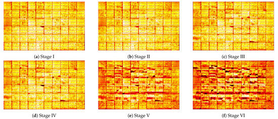
Figure 1.
Electroluminescence (EL) images of module #1, measured at Standard Test Conditions (STC) Isc current bias, before the accelerated stress test (Stage I), and after each stress stage described in Table 1. Brighter image areas correspond to cell regions with higher luminescence, whereas darker areas correspond to low or no luminescence emissions
After each stress-test stage, the modules were flash tested under STC and low irradiance conditions (LIC, 200 W/m2, 25 °C). The STC and low light degradation is summarized in Figure 2. Here we observe a final STC power degradation between 8% and 10.4 %, and between 5.5 % to 7 % LIC power loss.
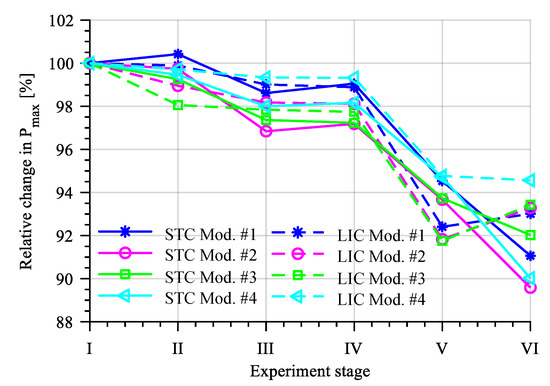
Figure 2.
Relative change in the STC and low light maximum power of the fours test samples during the six stages of degradation.
The corresponding light I-V curves for module #1 are shown in Figure 3a, where we can observe fill factor and short-circuit current losses to a lower extent. Whereas, the dark I-V characteristics of module #1, shown in Figure 3b, show changes in both the high and low current regions of the dark I-V curve, associated with increased series resistance [15] and shunt and recombination losses [16], respectively. The electrical characteristics and power loss of modules #2–#4 are shown in Appendix A.2, Figure A4, Figure A5, Figure A6 respectively.
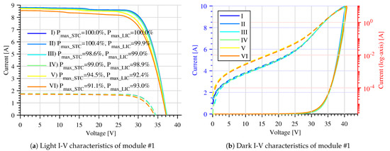
Figure 3.
Electrical characteristics and relative maximum power loss of module #1 measured during the accelerated stress test: (a) light I-V characteristics measured at STC and low irradiance conditions (LIC, 200 W/m2); (b) dark I-V characteristics of module #1 measured at 25 °C.
By examining the STC I-V curve parameters, we observe that the STC , summarized in Figure 4 for all four modules, contributes the most to the module performance degradation, which can be attributed primarily to the partial solar cell cracks, that increase the cells series resistance. Whereas a small decrease in can be observed for module #1, and to a lesser extent in modules #2 and #3, which can be attributed to a reduced photo-current generating cell area, due to fully disconnected cell cracks.
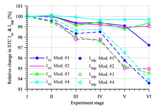
Figure 4.
Relative change in the STC short-circuit and maximum power point currents of the four modules during the six stages of the experiment—described in Table 1.
In addition, the modules show voltage losses in the later stages of the experiment (V and VI), shown in Figure 5, whereas the does not change significantly. Considering that the ratio decreases in these stages as well, we can deduce that these losses are caused (at least in part) by an increase in series resistance [17].
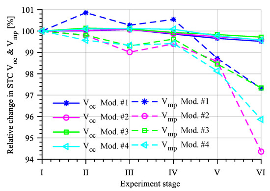
Figure 5.
Relative change in the STC open-circuit and maximum power point voltages of the four modules during the six stages of the experiment—described in Table 1.
To further understand the modes of degradation associated with this type of stress, we analyze the equivalent solar cell parameters of the modules during degradation [18]. To achieve this we fit the dark I-V curves () of the modules taken after each experiment stage to the two-diode solar cell model (1), often used for dark I-V based solar cell diagnostics [15]:
where J is the current density; V is the terminal voltage; and are the diode ideality factors; and are area-specific series and shunt resistance parameters, respectively, of the solar cell; T is the cell temperature; k is the Boltzmann constant; and q is the elementary charge.
The effect of the module degradation on the equivalent solar cell model parameters is summarized in Figure 6. From these results, we can confirm a substantial increase in module series resistance , previously observed in the I-V parameters and caused by partial solar cell cracks and metallization breaks [14]. Moreover, from Figure 6 we can observe a significant increase in the and diode model parameters, suggesting solar cell junction degradation and recombination losses occurring in the junction. Lastly, the and diode model parameters increase to a lesser extent. This increase can be attributed here to increasing defects and unpassivated surfaces at the cell cracks, causing increased surface and bulk recombination losses.
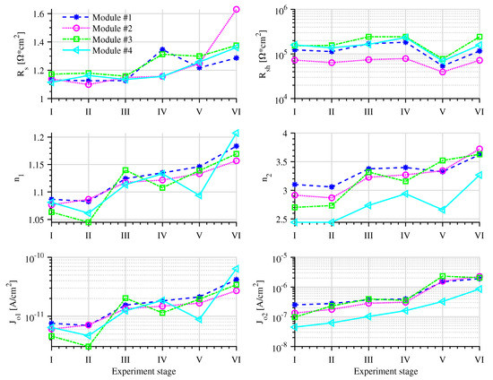
Concluding on the analysis of the diode model parameters, we can group the power loss mechanisms into three categories: (i) shunting and recombination losses, (ii) series resistance losses, (iii) other losses including recombination losses, current mismatch losses, and a decrease in photo-current generation due to cell fracturing. In the next section we aim to estimate these failure modes’ effect on the module STC power loss separately.
3. In-situ STC Power Loss Estimation Method
3.1. Step 1—In-Situ during Stress Testing—Estimate the Effects of Recombination and Shunting Losses
The first step, estimating the power loss due to shunting and recombination losses, has been previously studied for crystalline silicon modules undergoing PID-s [7,19]. In this case, module STC degradation can be estimated with high accuracy in-situ, by superposition of the dark I-V curve with measured [7]. Some limitations of the method include modules that are severely shunted, for which the current starts to decrease significantly [20] and superposition using the initial is no longer valid.
We assume that module dark I-V characteristics are measured at 25 °C during the test. This is a feasible assumption for mechanical loading tests that are carried out at room temperature, as well as for thermal cycling and humidity freeze type tests, where the 25 °C dark I-V characteristic can be measured at the beginning/end of the cycle, when the chamber and module temperatures are ramped up/down.
Based on the 25 °C dark I-V curve we can estimate the module STC that accounts for the effects of shunting and losses, by superposition of the dark I-V curve with , and calculating the maximum power point from the resulting I-curve, as expressed in (2):
where is the dark I-V characteristic of the module measured measured at 25 °C and at a time point t during the stress test, and is the initial STC current of the module measured on a Sun simulator.
3.2. Step 2—In-Situ during Stress Testing—Estimate (Partial) Series Resistance Losses from Dark I-V Measurements
In the next step we need to estimate the increase in series resistance due to cell cracks, from the dark I-V measurements acquired in-situ, and use it to correct the superposition estimated power loss accordingly. This could be achieved by curve fitting the diode model parameters () in (1), which requires careful parametrization of the initial conditions and does not lend itself to automatic analysis during the stress test.
Alternatively, increases in the module’s dark series resistance can be estimated from the slope of the dark I-V curve at high current (), as in (3), which is linearly related to the module’s , not including diode-internal voltage drops [21].
Next, to estimate the power loss due to the increased series resistance, we start from the empirical equations for calculating the effect of increased series resistance on the fill factor of solar cells [22], defined in (4):
where is the normalized PV module series resistance, is the fill factor without the effect of series resistance, and is the corrected PV module fill factor, including series resistance losses.
If we consider to only represent the increase in the module’s series resistance since the test has started (), we can define as a function of , determined in-situ, and the initial STC parameters of the module: and , as in (5):
3.3. Step 3—Adjustment with Final Light I-V Curve—Estimate the Total Series Resistance and Other Losses from a Final STC Flash Test
There are two limiting factors for estimating series resistance from the dark I-V characteristic of the PV module that must be considered. First, when measuring the dark I-V characteristic, the current paths through the module are more limited in area compared to when the module is illuminated [23]. This situation leads to two different module values, dark and light measured, where generally the dark-measured is be smaller than the light-determined resistance. Consequently, use of the dark I-V curve-determined series resistance, such as , will underestimate the STC losses due to increases in . Second, does not explicitly include the effect of decreased current generation and mismatch due to cell fracturing or the increase in recombination losses that can appear around in the dark I-V curve and can lead to additional errors in estimating the STC .
To compensate for the limitation of the dark estimated series resistance, in the final step is adjusted such that the final degradation, which is estimated from dark I-V measurements, matches the final STC degradation that is measured by a Sun simulator. This problem can be formulated for solution as in (7), where and are the initial and final 25 °C dark I-V curve and STC power () measurements points:
By numerically solving (7) for , we can determine a value, which will account for both the increase in module (light) , as well as other losses, such recombination and current mismatch losses due to cell fracturing, occurring in the module after the previous experiment stage. The is then used to adjust each intermediate with (8):
4. Results and Discussion
We experimentally evaluate the accuracy and limits of the in-situ power loss estimation procedure, by comparing the PV module power losses determined in the three steps of the proposed method, with measured module power loss.
First we determine the extent of power loss due to shunting and losses, by calculating from (2), using the measured at at 1000, 600, and 200 W/m2 irradiance, and 25 °C. The relative change in of module #1 is shown in Figure 7, versus the Sun simulator measured power of the module, denoted as , under the same irradiance conditions. We can observe that the dark I-V superposition-based power loss estimation is poor, especially under high irradiance conditions and extensive degradation (up to 6% difference in relative power loss). This can be explained by the increased series losses that are not captured by the superposition method.
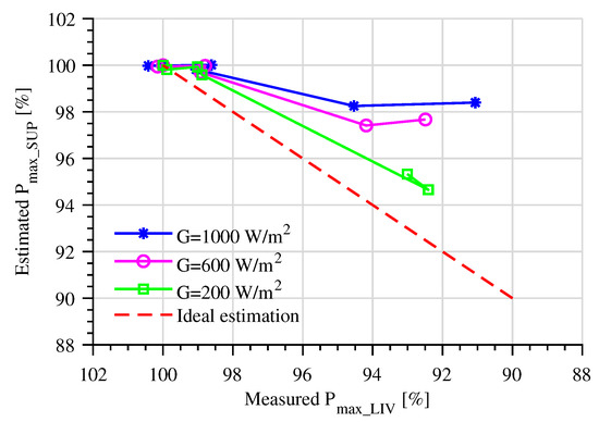
Figure 7.
Estimated module #1 power loss by simple dark I-V superposition (), versus actual measured power loss (), at 1000, 600, and 200 W/m2 irradiance.
Similar trends can be observed by comparing STC of the other module samples with their measured shown in Figure 8. As the modules degrade more by cell cracking, the estimation error increases. We can surmise that the shunting and losses amount to up to 2% of the absolute power loss, explaining up to 30% of the power loss exhibited.
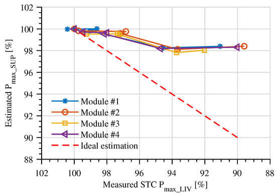
Figure 8.
Comparison of estimated module power loss by simple dark I-V superposition (), versus measured STC power loss (), for all four modules.
Next, to evaluate the extent of increased series resistance losses, we determine the increase in from 25 °C dark I-V measurements and use it to estimate the relative module power loss (), according to (5) and (7). Figure 9 shows the estimated power loss for module #1. It can be observed that the estimation has improved only slightly, however at 5% STC degradation (stage V), underestimates the module #1 degradation by 3% (absolute error), whereas at 10% module degradation (stage VI), the difference between the dark vs. light measured module power degradation can be as much as 5% (absolute error). This is explained by the limited capability of to characterize the light series resistance, as well as the impact of losses on the module STC power.
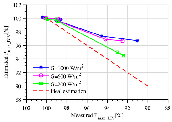
Figure 9.
Estimated module #1 power loss by dark I-V superposition () and series resistance compensation (dark I-V estimated—), versus actual measured power loss (), at 1000, 600, and 200 W/m2 irradiance.
Similar estimation errors are observed for the other modules shown in Figure 10, with the exception of module #3, which is closest to the ideal estimation line. One possible explanation is that module #3 had the least losses among the four modules tested, as can be observed from Figure 4.
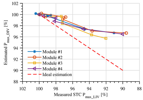
Figure 10.
Comparison of estimated module power loss by dark I-V superposition () and series resistance compensation (dark I-V estimated - ), versus actual measured STC power loss (), for all for modules
The module power loss estimation must be improved by the final STC adjustment, as in (7) and (8), which will compensate for most of the current mismatch, decrease in and photocurrent-generation, and other losses such as recombination losses, which are difficult to characterize from the dark I-V curve alone. These findings are consistent with previous research on methods for estimating PV module series resistance [24], that have concluded that dark series resistance underestimated the light determined series resistance by more than 50%, in most cases [24].
To exemplify the adjustment procedure, we used the initial and final STC flash test to calculate the correction factor from (7), and use it to adjust the dark I-V-determined series resistance () as in (8). The resulting as well as are compared in Figure 11, with the STC flash test determined resistance of module #1, calculated after each stress stage. As can be observed, stages V and VI show a significant increase in the module’s series resistance that is not captured by , but can be compensated for, by the final STC flash test, and thus included in .
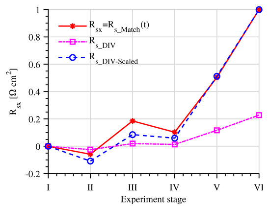
Figure 11.
Comparison of the three PV module series resistance procedures, exemplified for PV module #1: - series resistance estimated from the dark I-V as in (3); - series resistance estimated by matching the final STC I-V as in (6) and (7); - series resistance estimated by scaling with the final as in (8).
Finally, is calculated by substituting in (6), and is compared with the STC measured in Figure 12. As can be observed, this approach leads to a more successful estimation of the module degradation, especially in the later stages of the experiment.
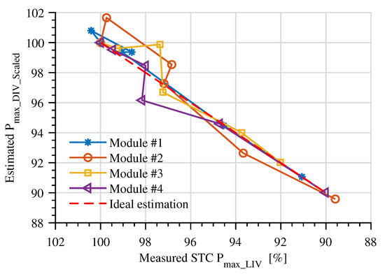
Figure 12.
Comparison of degradation versus measured STC of the four modules.
The errors between the and STC in the early stages of degradation result from the approximation that scales linearly with the light series resistance, assumed in (8). Second, flash test and dark I-V measurement errors are compounded, such that individual points in Figure 12 may be affected. Despite these limitations, if we compare the root-mean-square error (RMSE) between the STC measured , and the dark I-V estimated , as in Table 2 we can observe the final adjustments of the series resistance based on flash testing, and reduce the total estimation error by 3–6 times.
Table 2.
Comparison of root-mean-square error (RMSE) between the STC measured , and the dark I-V estimated ( – only shunting and losses are estimated; —series losses are estimated as well; —other losses are estimated with a final STC power match).
5. Conclusions
Tools and methods for monitoring PV module degradation, in-situ, during accelerated stress testing, are important for understanding the degradation kinetics and developing reliability and accelerated degradation modules, as well as for reducing the cost, duration and effort of accelerated stress tests.
In this regard, in-situ acquired dark I-V curves have previously been used to successfully monitor PID-s during voltage stress testing of c-Si PV modules, and were the basis of the in-situ monitoring method proposed in this work. However monitoring thermo-mechanical induced degradation of PV modules by dark I-V measurements is more challenging, due to the complex nature of the induced degradation modes. Namely, thermo-mechanical stress can compound several failure modes: micro-cracking, partial or complete cell cracking and disconnection, cell interconnect failure, and even delamination. These will affect cells in the modules to different extents, and are sometimes difficult to deconvolute from module level I-V characteristics or by equivalent solar cell model parameters, as the basic assumption of identical cells in the module is broken.
Part of the power loss caused by cell cracking—corresponding to shunting and junction recombination, can be estimated by superposition of the dark I-V with initial module short-circuit current, similar to the in-situ PID power loss estimation method. However, the majority of power loss caused by cell cracking is caused by an increase in the module’s distributed series resistance, which is not well captured by the dark I-V curve superposition method.
As was shown, part of the module’s increased series resistance can be estimated from the dark I-V characteristic, however, not completely. A final STC IV measurement, at the end of the stress test, is necessary to correct the dark I-V power loss estimation. However, module delamination and short-circuit current degradation, occurring during the stress test, will reduce the estimation accuracy of the in-situ method, for intermediate points of degradation. Therefore, for longer thermo-mechanical stress tests, intermediate flash tests would be necessary to correct the power loss estimation in these cases, or another in-situ measurement that is able to characterize degradation of the module’s photo-current generation properties.
Author Contributions
Conceptualization, P.H., S.S. and D.S.; methodology, S.S. and P.H.; software, S.S.; validation, S.S., and P.H; formal analysis, P.H.; investigation, S.S. and P.H.; resources, D.S. and P.H.; data curation, S.S.; writing–original draft preparation, S.S. and P.H.; writing–review and editing, S.S., P.H. and D.S.; visualization, S.S.; supervision, D.S. and P.H.; project administration, P.H. and D.S.; funding acquisition, P.H. and D.S. All authors have read and agreed to the published version of the manuscript.
Funding
The work carried out at NREL was supported by the U.S. Department of Energy under Contract No. DE-AC36-08-GO28308 with the National Renewable Energy Laboratory.
Acknowledgments
The authors thank Greg Perrin and Kent Terwilliger for their help performing the experiments, and Steve Rummel for module measurements.
Conflicts of Interest
The authors declare no conflict of interest.
Appendix A
Appendix A.1. Electroluminescence Images of Modules 2–4

Figure A1.
EL images of module #2, measured at STC Isc current bias, before the accelerated stress test (Stage I), and after each stress stage described in Table 1. Brighter image areas correspond to cell regions with higher luminescence, whereas darker areas correspond to low or no luminescence emissions.


Figure A2.
EL images of module #3, measured at STC Isc current bias, before the accelerated stress test (Stage I), and after each stress stage described in Table 1.
Figure A2.
EL images of module #3, measured at STC Isc current bias, before the accelerated stress test (Stage I), and after each stress stage described in Table 1.


Figure A3.
EL images of module #1, measured at STC Isc current bias, before the accelerated stress test (Stage I), and after each stress stage described in Table 1.
Figure A3.
EL images of module #1, measured at STC Isc current bias, before the accelerated stress test (Stage I), and after each stress stage described in Table 1.

Appendix A.2. Light and Dark I-V Characteristics of Modules 2–4

Figure A4.
Electrical characteristics and relative maximum power loss of module #2 measured during the accelerated stress test: (a) light I-V characteristics measured at STC and low irradiance conditions (LIC, 200 W/m2); (b) dark I-V characteristics of module #2 measured at 25 °C.
Figure A4.
Electrical characteristics and relative maximum power loss of module #2 measured during the accelerated stress test: (a) light I-V characteristics measured at STC and low irradiance conditions (LIC, 200 W/m2); (b) dark I-V characteristics of module #2 measured at 25 °C.


Figure A5.
Electrical characteristics and relative maximum power loss of module #3 measured during the accelerated stress test: (a) light I-V characteristics measured at STC and low irradiance conditions (LIC, 200 W/m2); (b) dark I-V characteristics of module #3 measured at 25 °C.
Figure A5.
Electrical characteristics and relative maximum power loss of module #3 measured during the accelerated stress test: (a) light I-V characteristics measured at STC and low irradiance conditions (LIC, 200 W/m2); (b) dark I-V characteristics of module #3 measured at 25 °C.


Figure A6.
Electrical characteristics and relative maximum power loss of module #4 measured during the accelerated stress test: (a) light I-V characteristics measured at STC and low irradiance conditions (LIC, 200 W/m2); (b) dark I-V characteristics of module #4 measured at 25 °C.
Figure A6.
Electrical characteristics and relative maximum power loss of module #4 measured during the accelerated stress test: (a) light I-V characteristics measured at STC and low irradiance conditions (LIC, 200 W/m2); (b) dark I-V characteristics of module #4 measured at 25 °C.

References
- Masuda, A.; Yamamoto, C.; Uchiyama, N.; Ueno, K.; Yamazaki, T.; Mitsuhashi, K.; Tsutsumida, A.; Watanabe, J.; Shirataki, J.; Matsuda, K. Sequential and combined acceleration tests for crystalline Si photovoltaic modules. Jpn. J. Appl. Phys. 2016, 55, 04ES10. [Google Scholar] [CrossRef]
- Carlsson, T.; Halme, J.; Lund, P.; Konttinen, P. Moisture sensor at glass/polymer interface for monitoring of photovoltaic module encapsulants. Sens. Actuators A Phys. 2006, 125, 281–287. [Google Scholar] [CrossRef]
- Tanahashi, T.; Suzuki, S.; Sakamoto, N.; Mito, A.; Shirasawa, K.; Takato, H. In Situ ac impedancemeasurement in c-Si PVmodules during rapid thermal cycling test. In Proceedings of the 2015 Photovoltaic Module Reliability Workshop, Golden, CO, USA, 24–27 February 2015. [Google Scholar]
- Bosco, N.; Silverman, T.J.; Wohlgemuth, J.; Kurtz, S.; Inoue, M.; Sakurai, K.; Shioda, T.; Zenkoh, H.; Hirota, K.; Miyashita, M.; et al. Evaluation of Dynamic Mechanical Loading as an accelerated test method for ribbon fatigue. In Proceedings of the 2013 IEEE 39th Photovoltaic Specialists Conference (PVSC), Tampa, FL, USA, 16–21 June 2013; pp. 3173–3178. [Google Scholar] [CrossRef]
- Sander, M.; Dietrich, S.; Pander, M.; Ebert, M.; Bagdahn, J. Systematic investigation of cracks in encapsulated solar cells after mechanical loading. Sol. Energy Mater. Sol. Cells 2013, 111, 82–89. [Google Scholar] [CrossRef]
- Owen-Bellini, M.; Sulas-Kern, D.B.; Perrin, G.; North, H.; Spataru, S.; Hacke, P. Methods for In Situ Electroluminescence Imaging of Photovoltaic Modules Under Varying Environmental Conditions. IEEE J. Photovoltaics 2020, 10, 1254–1261. [Google Scholar] [CrossRef]
- Hacke, P.; Smith, R.; Terwilliger, K.; Glick, S.; Jordan, D.; Johnston, S.; Kempe, M.; Kurtz, S. Testing and Analysis for Lifetime Prediction of Crystalline Silicon PV Modules Undergoing Degradation by System Voltage Stress. IEEE J. Photovoltaics 2013, 3, 246–253. [Google Scholar] [CrossRef]
- Spataru, S.; Hacke, P.; Sera, D.; Packard, C.; Kerekes, T.; Teodorescu, R. Temperature-dependency analysis and correction methods of in situ power-loss estimation for crystalline silicon modules undergoing potential-induced degradation stress testing. Prog. Photovoltaics Res. Appl. 2015, 23, 1536–1549. [Google Scholar] [CrossRef]
- Luo, W.; Hacke, P.; Singh, J.P.; Chai, J.; Wang, Y.; Ramakrishna, S.; Aberle, A.G.; Khoo, Y.S. In-Situ Characterization of Potential-Induced Degradation in Crystalline Silicon Photovoltaic Modules Through Dark I–V Measurements. IEEE J. Photovoltaics 2016, 7, 104–109. [Google Scholar] [CrossRef]
- Lindholm, F.A.; Fossum, J.G.; Burgess, E.L. Application of the superposition principle to solar-cell analysis. IEEE Trans. Electron Devices 1979, 26, 165–171. [Google Scholar] [CrossRef]
- Kawai, S.; Tanahashi, T.; Fukumoto, Y.; Tamai, F.; Masuda, A.; Kondo, M. Causes of Degradation Identified by the Extended Thermal Cycling Test on Commercially Available Crystalline Silicon Photovoltaic Modules. IEEE J. Photovoltaics 2017, 7, 1511–1518. [Google Scholar] [CrossRef]
- Du, Y.; Wang, L.; Tao, W. Modeling, imaging and resistance analysis for crystalline silicon photovoltaic modules failure on thermal cycle test. Eng. Fail. Anal. 2020, 118, 104818. [Google Scholar] [CrossRef]
- Mölken, J.I.V.; Yusufoğlu, U.A.; Safiei, A.; Windgassen, H.; Khandelwal, R.; Pletzer, T.M.; Kurz, H. Impact of Micro-Cracks on the Degradation of Solar Cell Performance Based On Two-Diode Model Parameters. Energy Procedia 2012, 27, 167–172. [Google Scholar] [CrossRef]
- Köntges, M.; Kunze, I.; Kajari-Schröder, S.; Breitenmoser, X.; Bjørneklett, B. The risk of power loss in crystalline silicon based photovoltaic modules due to micro-cracks. Solar Energy Mater. Sol. Cells 2010, 95, 1131–1137. [Google Scholar] [CrossRef]
- King, D.; Hansen, B.; Kratochvil, J.; Quintana, M. Dark current-voltage measurements on photovoltaic modules as a diagnostic or manufacturing tool. In Proceedings of the 26th IEEE Photovoltaic Specialists Conference, Anaheim, CA, USA, 29 September–3 October 1997; pp. 1125–1128. [Google Scholar] [CrossRef]
- Meyer, E.; van Dyk, E. Assessing the Reliability and Degradation of Photovoltaic Module Performance Parameters. IEEE Trans. Reliab. 2004, 53, 83–92. [Google Scholar] [CrossRef]
- King, D.L.; Quintana, M.A.; Kratochvil, J.A.; Ellibee, D.E.; Hansen, B.R. Photovoltaic module performance and durability following long-term field exposure. Prog. Photovoltaics Res. Appl. 2000, 8, 241–256. [Google Scholar] [CrossRef]
- Wolf, M.; Noel, G.T.; Stirn, R.J. Investigation of the double exponential in the current—Voltage characteristics of silicon solar cells. IEEE Trans. Electron Devices 1977, 24, 419–428. [Google Scholar] [CrossRef]
- Lausch, D.; Naumann, V.; Breitenstein, O.; Bauer, J.; Graff, A.; Bagdahn, J.; Hagendorf, C. Potential-Induced Degradation (PID): Introduction of a Novel Test Approach and Explanation of Increased Depletion Region Recombination. IEEE J. Photovoltaics 2014, 4, 834–840. [Google Scholar] [CrossRef]
- Pingel, S.; Frank, O.; Winkler, M.; Daryan, S.; Geipel, T.; Hoehne, H.; Berghold, J. Potential Induced Degradation of solar cells and panels. In Proceedings of the 2010 35th IEEE Photovoltaic Specialists Conference, Honolulu, HI, USA, 20–25 June 2010; pp. 2817–2822, ISSN 0160-8371. [Google Scholar] [CrossRef]
- Zeghbroek, B.V. Chapter 4: p-n Junctions. In Principles of Semiconductor Devices. Bart Van Zeghbroek. 2011. Available online: http://ecee.colorado.edu/~bart/book/book/chapter4/ch4_4.htm (accessed on 10 October 2020).
- Green, M.A. Accuracy of analytical expressions for solar cell fill factors. Solar Cells 1982, 7, 337–340. [Google Scholar] [CrossRef]
- Bowden, S.; Rohatgi, A. Rapid and Accurate Determination of Series Resistance and Fill Factor Losses in Industrial Silicon Solar Cells. In Proceedings of the 17th European Photovoltaic Solar Energy Conference and Exhibition, Munich, Germany, 22–26 October 2001; p. 5. [Google Scholar]
- Pysch, D.; Mette, A.; Glunz, S. A review and comparison of different methods to determine the series resistance of solar cells. Solar Energy Mater. Sol. Cells 2007, 91, 1698–1706. [Google Scholar] [CrossRef]


Publisher’s Note: MDPI stays neutral with regard to jurisdictional claims in published maps and institutional affiliations. |
© 2020 by the authors. Licensee MDPI, Basel, Switzerland. This article is an open access article distributed under the terms and conditions of the Creative Commons Attribution (CC BY) license (http://creativecommons.org/licenses/by/4.0/).