1. Introduction
With the development of technology, batteries have been extensively used in daily life. Batteries are used in electric vehicles [
1,
2,
3], wearable devices, and large energy storage systems [
4,
5,
6]. Therefore, the efficiency, life, and reliability of batteries are becoming increasingly critical. A battery management system (BMS) [
7,
8,
9] is widely used to improve the utilization of batteries. Apart from preventing overcharge and over-discharge of batteries, BMS diagnoses and analyzes battery life and health status by recording battery-related data and residual capacity to optimize their overall performance.
One of the standard test methods for batteries’ usable capacity is the coulomb measurement method [
10,
11]. This method is used to calculate the current value flowing into or out of batteries and integrates the current value over time to determine the number of coulombs flowing through. This method can accurately estimate the available battery capacity. In battery capacity measurement, the accuracy of voltage and current measurements is related to the final calculation error. To achieve an accurate battery capacity calculation, the battery charging current must be accurately measured. The current ripple elimination mechanism is particularly important to prevent the output current ripple from causing measurement errors and reduce the volume of the output capacitor to increase power density.
Standard current ripple elimination techniques are mainly divided into three categories. The first category uses multi-phase buck converters in parallel and alternately switched with one another [
12,
13]. Through the sum of the current ripples of different phases, the final synthesized overall output current can reduce the total ripple amount and period, thereby increasing the equivalent current ripple frequency to reduce the capacitance of the output capacitor. However, the combined current ripples with this approach can only cancel each other under a specific duty cycle and number of parallel connections, thereby achieving an ideal current ripple elimination effect. Moreover, the use of multiple units in parallel increases the circuit cost and layout area, and the current sharing between multiple converters also requires additional control [
14,
15], thereby increasing the overall complexity. The second category uses coupled inductors to generate reverse ripple current [
16,
17]. The coupled inductor automatically generates the reverse ripple current, and the current ripple cancellation function can be achieved under any duty cycle. However, this cancellation function is fundamentally a fourth-order LC filter [
18], which is based on filtering to obtain the characteristics of low output current ripple. A converter’s output current filtering capability and transient response often have opposite design indicators when designing a fourth-order LC filter. To achieve a superior filtering effect, the inductance value of the filter should be increased, which directly reduces the transient response speed of the converter. Therefore, the converter’s transient response will be fundamentally limited in the application of low current ripple output. The third category uses a stacked architecture [
19,
20], which utilizes the complementary operation of the upper and lower switches of the two bridge arms to superimpose the two arms’ inductor currents. In this way, the output inductor current ripple can be canceled under any switching duty cycle. This architecture can accelerate the rising or falling slope of the overall output current when both arms are turned on simultaneously on the upper or lower bridge switch, thereby improving the transient response. However, the literature [
19,
20] has only extensively discussed complementary switching signals. Moreover, these studies have not focused on the dead time of the upper and lower bridge switching signals in practical applications and the parasitic capacitance of switching elements. Consequently, the current ripple elimination effect is affected. The RC delay control method proposed in the pattern [
21] improves the transient response by increasing a converter’s transient response. However, this method has flaws. After the feedback compensator is saturated, the area where the switching signals of the two arms overlap simultaneously cannot be generated, and the ability to increase the transient response is lost. On the basis of the preceding literature discussion, this study proposes a low output ripple dead time modulation and boundary limit control methods to improve the stacked buck converter’s output current ripple elimination effect and increase the transient response.
The remainder of this paper is structured as follows.
Section 1 presents the research background and introduction.
Section 2 reviews the two architectures proposed in the literature [
16,
17] and briefly describes their operating principles. Thereafter, the coupling mutual inductance form is converted into a fourth-order LC filter form [
18]. The fourth-order filter is used to illustrate why the output current ripple filtering ability and transient response cannot be considered.
Section 3 reviews the stacked buck converter [
19] and explains its operation and current ripple elimination principle. Moreover, this section uses the perspective of large signals to describe the fastest response speed that the converter can provide when the signals overlap simultaneously.
Section 4 reviews the RC delay control method [
21] and explains its limitations. Thereafter, this restriction is used as a basis to propose a new type of control method called the boundary limit control method.
Section 4 also explains its principle and uses simulation to verify the effect of the boundary limit control method.
Section 5 presents the influence of the switching dead time and switching parasitic capacitance of the stacked buck converter on the current ripple elimination effect and proposes a mathematical analysis of the principle. The dead time modulation method and formulation of the modulation variables are verified using mathematical derivation and simulation to confirm the feasibility and effectiveness of this modulation method.
Section 6 organizes the small-signal model of the coupled-inductor stacked buck converter. The small-signal model contains the small-signal model under the general two-arm switch complementary operation and boundary limit control method to design closed-loop compensation. Lastly, simulations are used to show the transient response of the system under different compensators.
Section 7 implements a sample circuit. This section likewise measures the effect of the switching dead time modulation method on the current ripple elimination ability. Lastly,
Section 8 summarizes this research.
2. Review of the Two Architectures and the Process of Converting Them to a Fourth-Order LC Filter
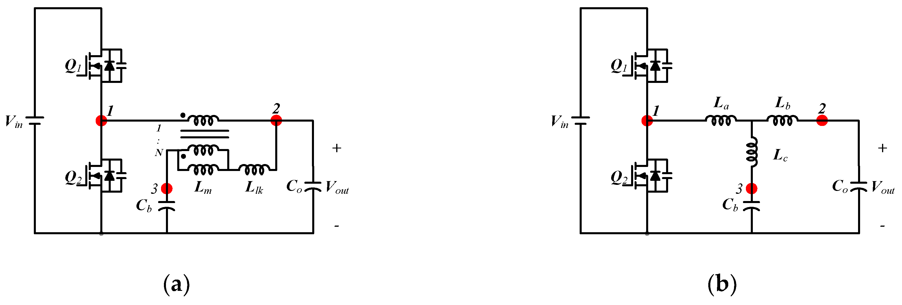
Figure 1 shows the circuit architecture and operation sequence diagram of the Ripple Current Cancellation Circuit (RCCC) [
16]. The entire architecture includes a blocking capacitor
Cb, coupled inductor, primary side magnetizing inductance
L1, secondary side equivalent leakage inductance
L2, and the primary and secondary turns ratio of 1:N.
From the steady-state volt-second balance of the equivalent leakage inductance
L2, the voltage on
Cb can be deduced to equal the output voltage
Vout. If
Cb and
Cout are assumed to be sufficiently large to disregard the voltage ripple on the capacitor, then the equations for
iL1,
iL2, and
i3 can be derived as follows:
To satisfy the ripple of the output current to zero amperes, the equation should be as follows:
By substituting Equations (1)–(3) into Equation (4), the relational equation can be derived as follows:
From Equation (5),
N can be obtained as follows:
When N satisfies Equation (6) in the RCC architecture, the output current can obtain the best elimination effect.
Figure 2 shows the circuit architecture diagram and operation sequence diagram of the three-terminal LL-LC network for current ripple cancellation (LL-LC) [
17]. The entire LL-LC architecture includes a blocking capacitor
Cb, coupled inductor, primary self-inductance
L1, secondary side self-inductance
L2, and a mutual inductance
M between the primary side and secondary side winding, and an external inductor
L3.
Figure 2 also shows that through the operating interval when switches
Q1 and
Q2 are turned on, Equations (7) and (8) can be respectively written as follows:
According to Kirchhoff’s Current Law (KCL) and Kirchhoff’s Voltage Law (KVL), the following two equations can be obtained:
In a steady-state operation, the average voltage across the inductor is zero. Hence, the voltage across
VCb is equal to the output voltage
Vout. Assuming that the
C3 capacitor is sufficiently large, its ripple can be disregarded. Equation (10) can be rewritten as follows:
When the inductance designed by L3 is equal to the mutual inductance M, the current change of iL1 in Equation (11) must be zero to satisfy this equation. Hence, iL1 can achieve the function of eliminating the current ripple.
RCCC and LL-LC can achieve zero current ripple output under the condition that the voltage ripple on the blocking capacitor is disregarded, and the ideal winding turns ratio and external inductance are ideally matched. However, this conclusion must be established on the fact that voltage ripple on blocking capacitor
Cb is minimal, and
Cb is simplified as a constant voltage source. In addition, the capacitance value is finite, given the blocking capacitor in the actual circuit. Given that the voltage ripple on the blocking capacitor must be considered, the two architectures’ actual effects on the elimination of the output current ripple should be re-discussed. A review of the circuit structure diagram of RCCC shows that the primary side inductance is equivalent to the secondary side, and the name of the capacitor and inductance is changed, as shown in
Figure 3a. Furthermore,
Figure 3b shows that the RCCC equivalent circuit diagram of the transformer model changed to the T equivalent model.
To make a conversion between the transformer and T-type equivalent models, the three nodes marked on the transformer in
Figure 3 must be described, and the impedance of any two nodes should be observed. Hence, the following three equations can be obtained:
Equations (12)–(14) show that
La,
Lb, and
Lc can be derived as follows:
In rewriting Equation (5), set
L1 = N−2Lm,
L2 = Llk, then:
The following equation is obtained when Equation (18) is substituted into Equation (17):
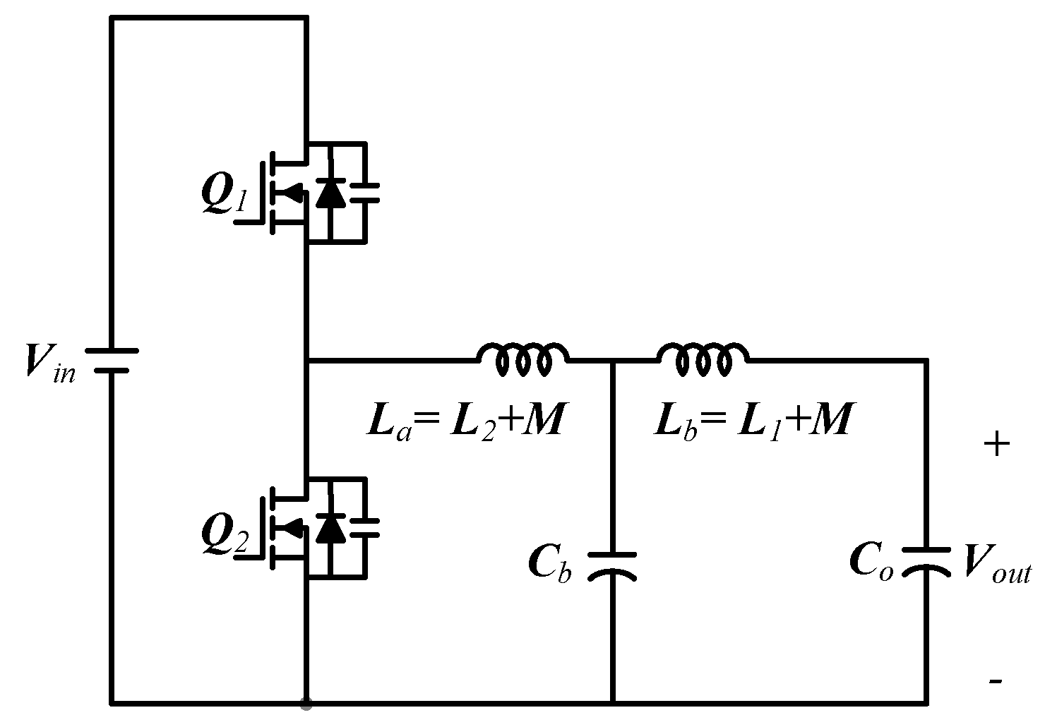
From the result of Equation (19),
Lc in the T-type model will become zero. The entire RCCC circuit will be converted into an LCLC fourth-order filter architecture, as shown in
Figure 4.
Using the same method, the coupled inductor in LL-LC is converted to a T-type model, as shown in
Figure 5.
To make a conversion between the transformer and T-type equivalent models, the three nodes marked on the transformer in
Figure 5 are described, and the impedance of any two nodes is presented. Thus, the following three equations can be obtained:
Equations (20)–(22) show that
La,
Lb, and
Lc can be deduced as follows:
Comparing the design in Equations (11) and (25), when
L3 = M, then:
The result of Equation (26) indicates that if the design conditions of LL-LC are met, then
Lc and
L3 in the T model will cancel each other out to zero. Furthermore, the entire LL-LC circuit will be converted into an LCLC fourth-order filter architecture, as shown in
Figure 6.
Two things can be learned in comparing the results of the conversion of RCCC and LL-LC into an equivalent fourth-order LCLC filter in
Figure 4 and
Figure 6. First, if the specific design conditions are met, then RCCC and LL-LC are essential fourth-order LCLC filters. Second, the ratios of
La and
Lb in the two equivalent fourth-order LCLC filters are not the same, but both have the function of current ripple filtering.
Given a fourth-order filter structure, the final filtering result of the output current ripple is determined by two aspects: (1) amount of ripple of the La inductor current and (2) ripple split ratio of Lb and Cb. To achieve an excellent current ripple filtering result, the inductance value of La should be considerably increased to reduce the inductance and capacitance values required by the current sharing circuit composed of Lb and Cb. Therefore, to pursue an excellent current ripple filtering effect for a fourth-order filter, the component value of the filter should be increased. However, such a design inevitably reduces the transient response of the converter.
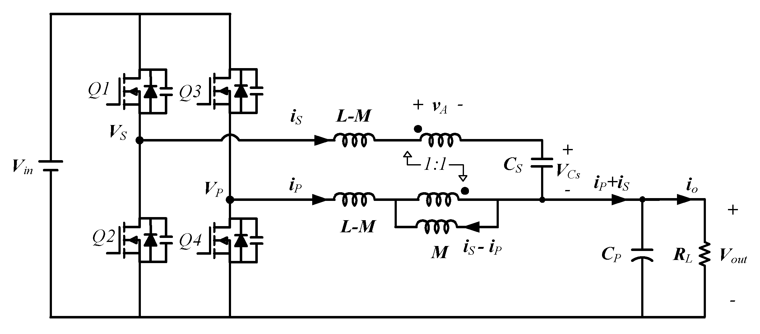
3. Review of the Stacked Buck Converter
Figure 7 shows the circuit structure and operation sequence diagram of the stacked buck converter [
19].
Q1,
Q2, and
Ls, and
CS and
CP in
Figure 7 constitute the first group of bucks, where
Q1 and
Q2 are collectively called P-arms. Moreover,
Q3,
Q4,
LP, and
CP form the second group of buck converters, among which
Q3 and
Q4 are collectively called the S-arms. The
iP current provides energy for the load, and the
iS current provides a reverse ripple current to cancel the ripple of the
iP current.
Compared to the two architectures reviewed in
Section 2, the stacked buck converter’s main idea is not to use a fourth-order filter to suppress the output current ripple. Therefore, substantial capacitance and inductance values are not required to suppress the output current ripple well. Therefore, the stacked buck converter can use a smaller inductor and capacitance value to achieve the same current ripple suppression effect. In other words, the stacked buck converter essentially has better transient response performance.
The duty cycle of Q3 as DP is defined. Given that the inductance LP satisfies the volt-second balance in the steady-state, Vout = DPVin can be obtained from the second group of buck converters. Vout + VCs = Vin(1 − DP) can be obtained from the first group of buck converters. Moreover, we can deduce that VCs = Vin(1 − 2DP).
When
Q2 and
Q3 are turned on, the current change slopes of
iP and
iS are respectively expressed as follows:
When
LP = LS = L, Equations (27) and (28) are added to obtain the following equation:
Evidently, Equation (29) is zero and does not contain the variable of the duty. The preceding derivation indicates that the cascaded buck converter can eliminate current ripples under any duty cycle. The stacked buck converter’s output current ripple elimination mechanism cancels the output current ripple by generating currents with opposite slopes from two sets of inductors. Such characteristics can ideally design the inductance value arbitrarily without affecting the output current ripple’s cancellation effect. To achieve an ideal current ripple elimination effect, the voltages of CS and CP should approximate the ideal voltage source. However, the transient response of the converter, in this case will have a detrimental effect.
If VCp is set as an ideal voltage source, then VCs is a variable capacitor voltage. Accordingly, VP + VS = Vin because the two arm switches are entirely complementary.
A review of Equation (29) indicates that if the slope of change of iP + iS is desired to be positive, then the voltage of VCs should be less than (1 − DP)Vin, which is below the steady-state value of the steady VCs voltage. That iss, when the CS capacitance is low, the voltage of VCs is considerably susceptible to the iS current, and the overall transient response of the converter is improved. However, this design concept will increase the ripple of VCs and reduce the effect of the current ripple elimination.
Compared with the fourth-order filter architecture, the stacked buck converter can use the upper or lower switches of the P and S arms to be turned on simultaneously to increase the transient response. Moreover, there is no need to deliberately reduce the capacitance of the
CS capacitor to sacrifice the current ripple elimination effect in exchange for the transient response speed. Review Equation (29) again, and substitute the
VP and
VS of Equation (29) into the input voltage
Vin, representing that the upper bridge switches of the P- and S-arms are turned on.
VCp and
VCs are regarded as ideal voltage sources, and the rate of change of
iP + iS is as follows:
If
VP and
VS are substituted into the ground level, then the lower bridge switches representing the P- and S-arms are turned on. Moreover,
VCp and
VCs are regarded as ideal voltage sources, and the rate of change of
iP + iS is as follows:
Equations (30) and (31) show that although VCs and VCp are constant voltage sources, the total inductor current change rate when the numerators of these equations are not zero can still be based on the control signal. Hence, VP = VS = Vin or VP = VS = 0 to achieve the rising or falling slope. Moreover, the design of L and M can adjust the magnitude of the change slope. By simultaneously turning on the upper or lower switches of the two arms, the stacked buck converter can retain the current ripple elimination characteristics and meet transient response needs.
4. Boundary Limit Control Method
The description in
Section 3 indicates that the stacked buck converter should be synchronized with the upper or lower bridge switches of the P- and S-arms to meet the transient response requirements.
To achieve this control interval, the literature [
21] has indicated that adding an RC delay circuit to the feedback compensation output
VEA of the original complementary controller can easily and simultaneously manufacture the upper and lower bridge switches of the P- and S-arms. The conduction period can improve the transient response.
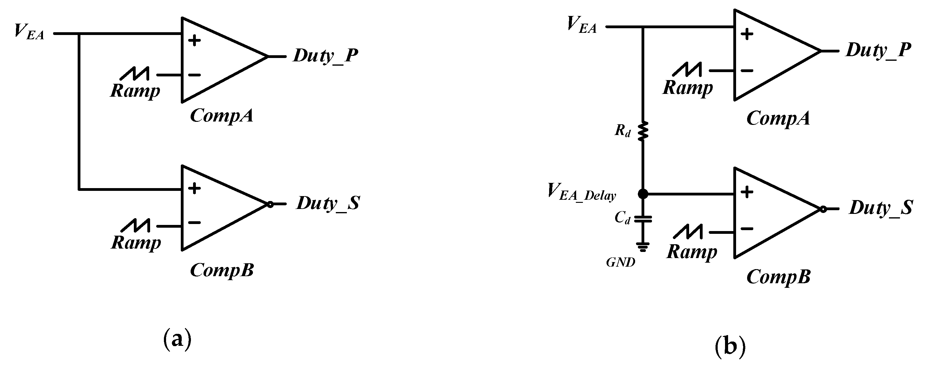
Figure 8a,b shows complementary and RC delay controllers, respectively.
Duty_P is the driving signal of the P-arm upper bridge switch
Q3, and
Duty_S is the driving signal of the S-arm upper bridge switch
Q1.
Figure 9 illustrates the operation sequence diagram of the RC delay type controller. When the output load increases, the compensator output
VEA changes from steady-state operation to positive saturation
VEA_sat, which is the operation sequence diagram of
VEA relative to PWM in this changing interval.
Figure 9 can be divided into three regions. Region I is the steady-state operation area, region II is the transient operation area, and region III is the saturation area. In region I,
VEA and
VEA_Delay can be regarded as the same signal, and
Duty_P and
Duty_S can be regarded as ideal complementary signals because the system reaches a steady-state. The output current ripple elimination mechanism is often operational. In region II, the output loading is increasing. The
VEA voltage begins to increase owing to the feedback system.
VEA and
VEA_Delay can no longer be regarded as the same signal because of the RC delay circuit, and the voltage amplitude
VEA is greater than
VEA_Delay. Therefore,
Duty_P and
Duty_S in region II have a duty overlap area, and the length of this area depends on the voltage difference between
VEA and
VEA_Delay. Duty overlap enables the converter to increase transient response. However, given that the system output voltage cannot stabilize immediately, the
VEA and
VEA_Delay voltages reach positive saturation and enter region III. In this region, the overlapping area of
Duty_P and
Duty_S disappears, returning to the general complementary operation, which significantly reduces the rising slope of the overall output current. However, the output load should receive energy at this time. Such an operation behavior further prolongs the time required for the output voltage to stabilize, and the depth of the output voltage undershoot increases. Therefore, the RC delay type control method cannot effectively adjust the converter’s output when the compensator reaches saturation.
Given the lack of RC delay control, this study proposes a boundary limit control method suitable for stacked buck converters. Apart from accelerating the transient response, the boundary limit control method is not limited by the saturation of the compensator.
Figure 10 shows a schematic of the boundary limit control method. The control principle aims to set the upper and lower limits of
VEA, and the limit value is fixed at the steady-state
VEA and take a settable boundary to generate a feedback compensation output
VEA_Limit.
Figure 11 shows the switch and control signal under the boundary limit control method. In region I,
VEA and
VEA_Limit maintain the same voltage because the system reaches a steady-state, and
Duty_P and
Duty_S maintain complementary operations. In region II,
VEA increases owing to an increase in load. When
VEA deviates from the steady-state
VEA value and the set limit boundary, the
VEA voltage is maintained, and
VEA_Limit is limited by the upper and lower limits. The result is the voltage difference between
VEA and
VEA_Limit, thereby making the duty of the P- and S-arm switches have an overlapping interval. In region III, although
VEA reaches positive saturation, the P- and S-arm switch signals maintain an overlapping interval because
VEA_Limit is limited, thereby continuously increasing the transient response of the system.
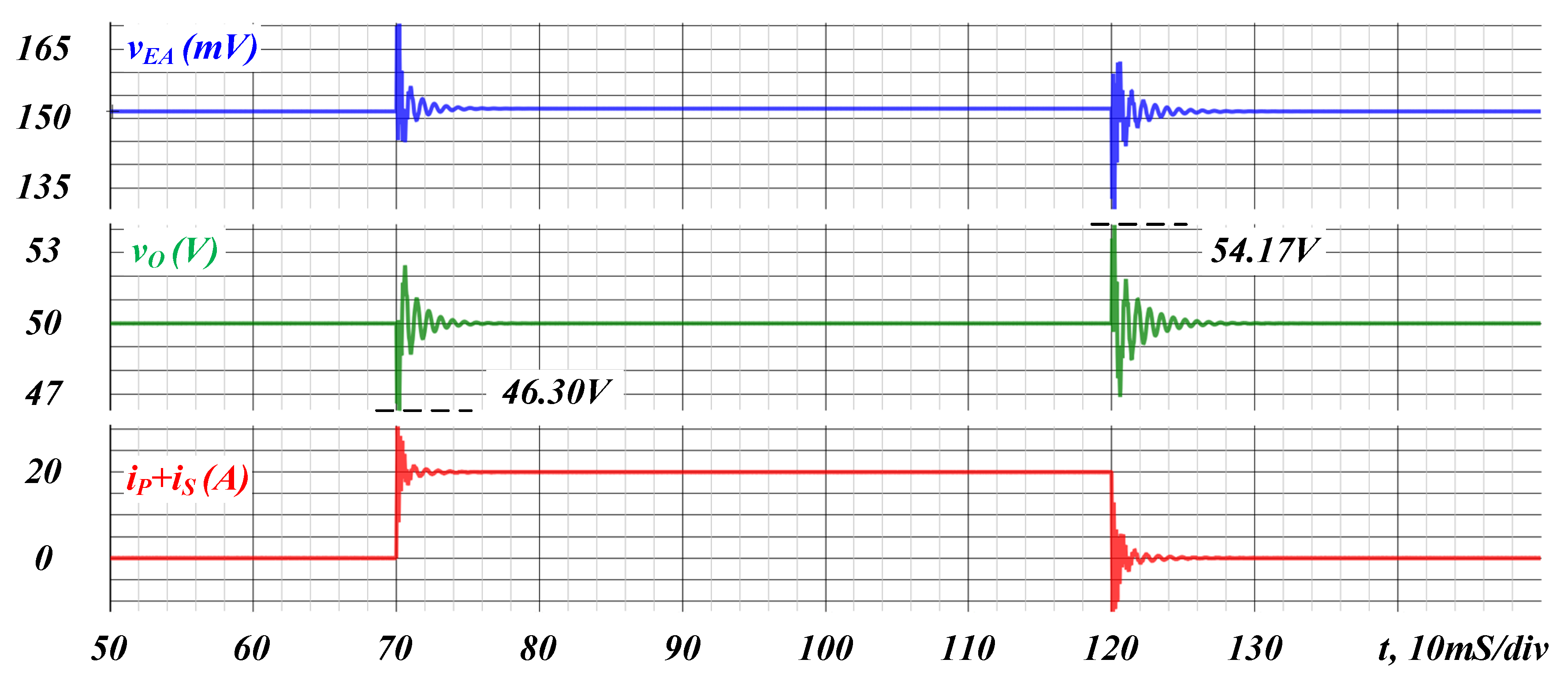
Figure 12 and
Figure 13 show the simulation results of the complementary and boundary limit controllers for the transient response. The system architecture diagram, circuit parameters, and compensator parameters are shown in
Table 1, and Equation (56), respectively. The load resistance switches from
RL = 2.5 Meg Ω to
RL = 2.5 Ω at t = 70 mS, and switches from
RL = 2.5 Ω to 2.5 Meg Ω again at t = 120 mS.
Figure 12 and
Figure 13 show that both control methods can achieve the effect of eliminating current ripples in the steady-state. Regarding the performance of the overshoot and undershoot of the output voltage, the boundary limit control method was superior to the complementary control method. Using the boundary limit control method to replace the complementary control method, the overshoot performance of the output voltage decreased from 417 mV to 361 mV, and the undershoot performance decreased from 370 mV to 324 mV.
5. Dead Time Modulation Method for Low Output Ripple
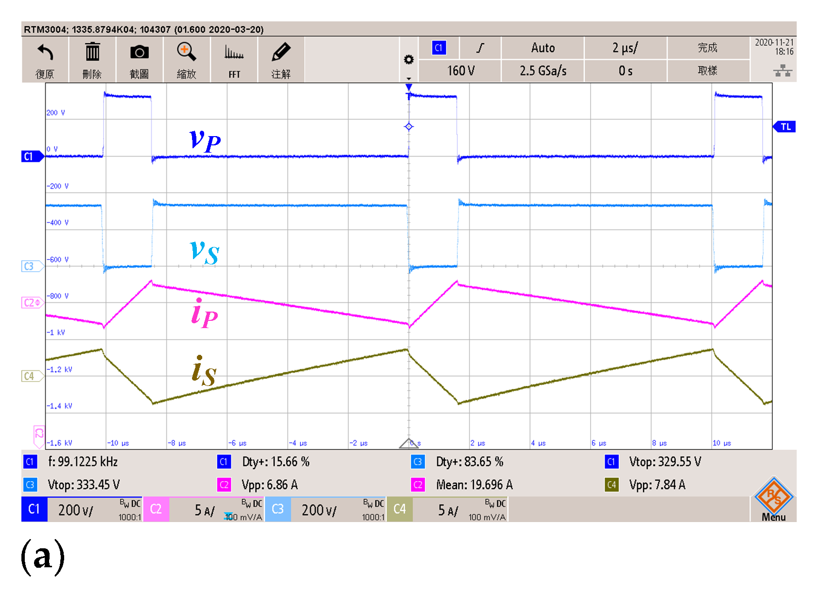
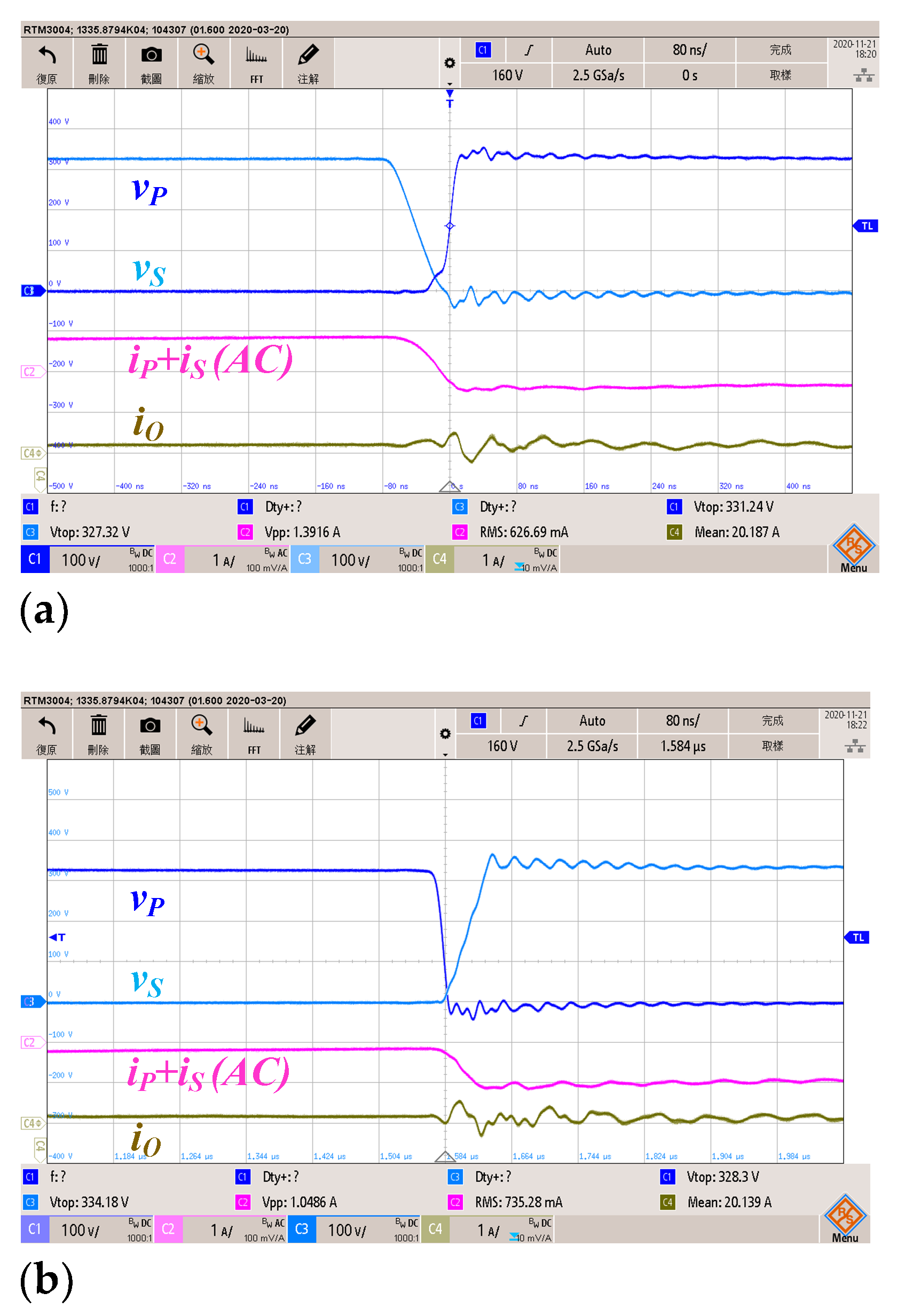
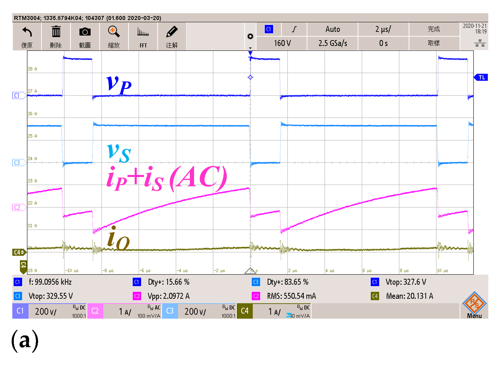
The output current ripple cancellation effect of the stacked buck converter in the existing system is affected by the actual dead time between the lower bridge switches. Hence, a necessary step is to understand the origin of the steady-state voltage value on the CS capacitor and the relationship between the voltage on the CS capacitor and the cancellation effect of the output current ripple.
Figure 14 shows the equivalent circuit diagram redrawn by converting the coupled inductor in
Figure 7a into a T-type model and unifying the symbols with
LS = LP = L.
To immediately understand and analyze the impact caused by dead time, the discussion of the circuit mode is limited to the idea that the output load condition is sufficiently large to make the current of iP constantly above zero.
To simplify the analysis, Vout and VCs can be regarded as fixed DC voltages by assuming that the capacitances of CP and CS are sufficiently large. In the dead time, the inductor L-M’s current change is small to be regarded as a constant current source. The switch’s parasitic capacitance Coss is fixed and does not change with the voltage across it. Moreover, the turn-on voltage drop of the body diode of the switch is disregarded as 0 V.
First, the steady-state voltage value of VCs is derived with an ideal stacked buck converter. Given that the switching signals are entirely complementary, the node voltages VP and VS have only two states: State 1, VS = Vin, VP = 0; and State 2, VS = 0, VP = Vin. Solving VCs for these two states, the derivation process is as follows.
State 1,
VS =
Vin,
VP = 0, according to KCL and KVL, the equation can be written as follows:
Substituting Equations (32) and (33) into Equation (34) can solve for
vA, and rename
vA in state 1 to
vA1. The resulting equation is as follows:
State 2,
VS = 0,
VP =
Vin, according to KCL and KVL, the equation can be written as follows:
Substituting Equations (36) and (37) into Equation (38) can solve for
vA, and rename
vA in state 2 to
vA2. The resulting equation is as follows:
The steady-state indicates that the inductance
M must satisfy the volt-second balance to write Equation (40), where
VA1 and
VA2 are the DC voltage levels obtained by the inverse Laplace conversion of
vA1 and
vA2, respectively, as follows:
Substituting Equations (35) and (39) into Equation (40) after the inverse Laplace transformation, we obtain the following equation:
Thereafter, solving Equation (41) can obtain
VCs as follows:
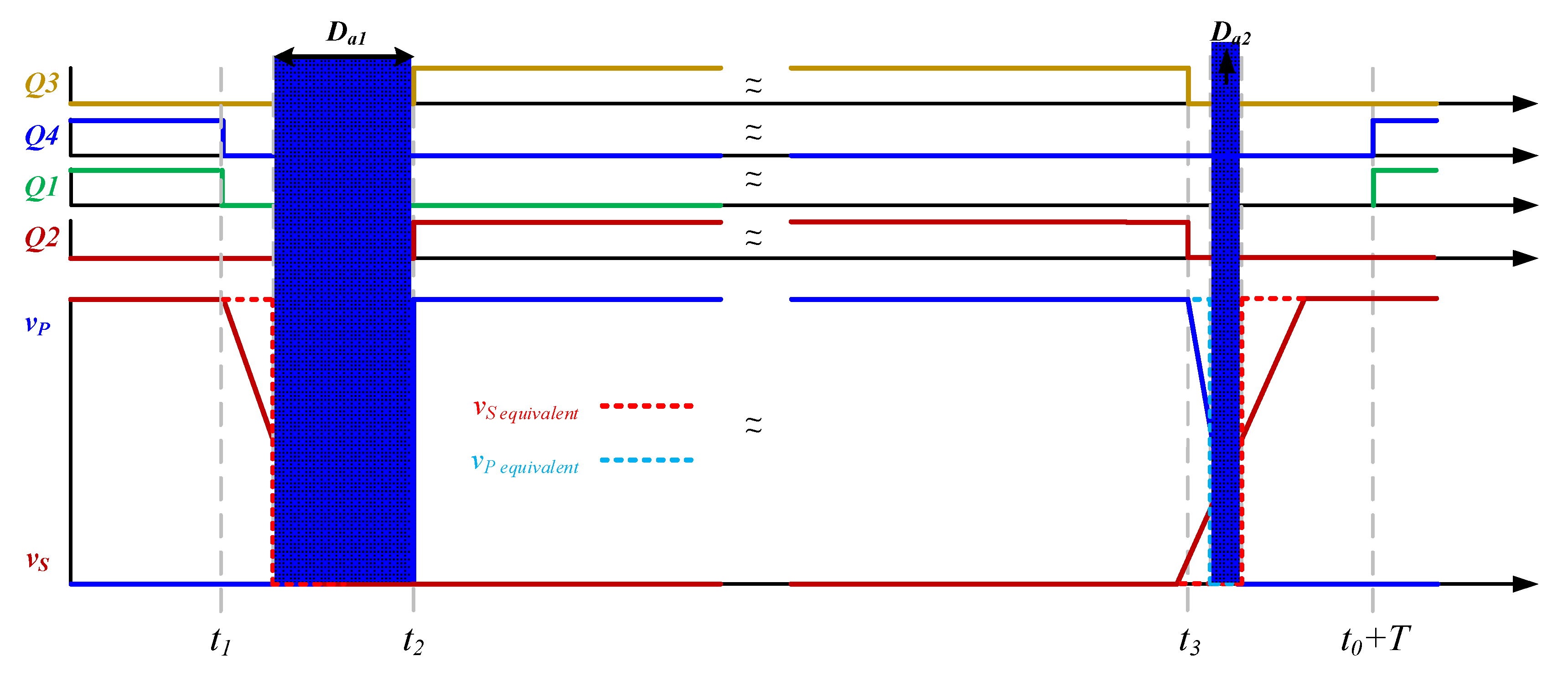
A review of Equation (29) indicates that when VP + VS − VCs = 2DPVin must be satisfied (i.e., when VCs = (1 − 2DP)Vin), the slope of iP + iS will be zero. In an ideal stacked buck converter, the relationship of Equation (29) is satisfied because the switching signals are completely complimentary. Hence, the output current ripple elimination behavior can be ideally achieved. However, in practical applications, the upper and lower bridge switches inevitably contain a dead time. Thus, the stacked buck converter’s current ripple elimination effect should be re-discussed.
Figure 15 shows an operation sequence diagram of a stacked buck converter with conventional dead time. Dead time is fixed, and four switches are turned off simultaneously. The operation sequence diagram in
Figure 15 can be divided into three sections: switch conduction section (
t0~t1,
t2~t3) and two different dead times (
t1~t2,
t3~t0+T).
The action sequence diagram shows that the ripple slope of iP + iS rises in the conduction interval of the two switches. In the two switch dead time intervals, the ripple slope change phenomenon of iP + iS is different, but both make iP + iS present an equivalent falling slope. Moreover, the voltage amplitude of VCs is slightly lower than (1 − 2DP)Vin.
The following discussion focuses on the three intervals to explain the behavior of the current ripple slope change of
iP + iS. To make the waveform more convenient for discussion, the two dead time intervals of
t1~t2 and
t3~t0+T in
Figure 15 are enlarged, leaving the
VP and
VS node voltage waveforms
vP and
vS, which are redrawn as
Figure 16.
First, we discuss the dead time interval (t1~t2).
When t = t1, all switches are off. Given that iP > 0, the current will automatically flow through the body diode of Q4 after switch Q4 is turned off. The vP voltage is maintained at 0 V until Q3 is turned on at t = t2 and the vP voltage increases vertically from 0V to Vin. Given that iS > 0, after Q1 is turned off, the iS current charges and discharges the Coss of Q1 and Q2. The initial value of the current is the peak value of the iS current. When the vS voltage decreases to 0 V, the body diode of Q2 turns on, clamping vS to 0 V. When t = t1, Q2 turns on and Vs continues to maintain 0 V.
Given that the current of is in the dead time is regarded as a fixed value, the voltage of vS decreases linearly. The vS discharge falling interval is taken as half of its falling time, and the equivalent vS waveform vS equivalent can be drawn. From the equivalent vS waveform, there is evidently a duty cycle Da1 between t = t1 and t = t2, and its equivalent vP and vS are 0 V.
From Equation (29), the slope of iP + iS is controlled by vP + vS − 2Vout − vCs. When vCs is equal to (1 − 2DP)Vin, and vP + vS is Vin, the current ripple offset can be achieved. However, in the dead time t = t1~t2 interval, except that vCs is slightly lower than (1 − 2DP)Vin, and vP + vS is smaller than Vin. Given that vP + vS − 2Vout − vCs < 0, the change slope of iP + iS during the entire dead time interval is negative.
Second, we discuss the dead time interval (t3~t0+T).
When t = t3, all switches are off. Given that iP > 0, after the switch, Q3 is turned off, the peak current of iP charges and discharges the Coss of Q3 and Q4. When the vP voltage drops to 0 V, the body diode of Q4 turns on and clamps vP to 0 V. When t = t0+T, Q4 turns on, and vP continues to maintain 0 V.
Note that the peak direct current of iP will change with load conditions. Thus, vP’s discharge slope will become rapid as load increases.
Given that iS < 0 after Q2 is turned off, the peak current of is charges and discharges Coss of Q1 and Q2. When the vS voltage rises to Vin, the body diode of Q1 is turned on, clamping vS to Vin; and when t = t0+T, Q1 is turned on and vS continues to maintain Vin. Moreover, given that the average current of iS is zero in the steady-state, the positive and negative peak currents of iS are equal in magnitude. Therefore, the time for the vS voltage in the dead time t = t3~t0+T to rise from 0 V to Vin is the same as the time for the vS voltage to fall from Vin to zero in the dead time t = t1~t2.
Given that the currents of iP and iS in the dead time are regarded as fixed values, vS and vP change voltages linearly. If half of the time of the voltage linear change of vP and vS, then the equivalent waveforms of vS and vP, vS equivalent and vP equivalent can be drawn. From the equivalent vS and equivalent vP waveforms, it can be observed that there is a duty period Da2 between time t3 and t0+T, and the equivalent vP and vS are both 0 V.
The slope of iP + iS is controlled by vP + vS − 2Vout − vCs. When vCS is equal to (1 − 2DP)Vin and vP + vS is Vin, the current ripple cancellation can be achieved. However, in the dead time t = t3~t0+T, except that vCs is slightly lower than (1 − 2DP)Vin, vP + vS = Vin after the body diodes of Q1 and Q4 are turned on. Therefore, in the dead time interval’s front and back zone, given that vP + vS − 2Vout − vCs > 0, the slope of change of iP+iS rises slightly. However, the equivalent vP and vS waveforms shows a Da2 equivalent duty cycle, and the vP and vS are both 0 V. The resulting falling slope of iP + iS is considerably larger than the other slight rising slopes. Hence, the overall iP+iS change continues to decrease in the dead time interval from t = t3~t0+T.
Lastly, we discuss the switch conduction interval (t0~t1, t2~t3):
The previous two dead time intervals show equivalent duty cycles
Da1 and
Da2. Hence,
vP and
vS are both 0 V. We define a new equivalent duty cycle
DA, where
DA = Da1+Da2. Given the converter’s new state, the previous derivation of
vA and
VCs should be imitated and
VCs voltage amplitude under the
DA duty cycle should be derived. From
Figure 14, we can deduce that the circuit equation of the circuit state under the
DA duty cycle is as follows.
State 3,
VS = 0,
VP = 0, according to KCL and KVL, the equations can be written as follows:
Substituting Equations (43) and (44) into Equation (45) can solve for
vA, and rename
vA in state 3 to
vA3 as follows:
According to the steady-state, the volt-second balance of the inductance
M can be written as Equation (47), where
VA1,
VA2, and
VA3 are the DC voltage levels obtained by the inverse Laplace transformation of
vA1,
vA2, and
vA3, respectively:
Substituting Equations (35) and (39) into Equation (40) after the inverse Laplace transformation can be obtained as follows:
Thereafter, solving (48) can obtain the modified equation of
VCs as follows:
From Equation (49), when DA > 0, VCs will be lower than (1 − 2DP)Vin. Although in the conduction interval (t0~t1, t2~t3), vP + vS = Vin, Equation (29) still cannot be established. Hence, the slope of iP + iS remains positive, and the ripple cannot be eliminated correctly.
This study proposes a dead time modulation method for low output ripple based on the preceding theoretical analysis. The modulation method is shown in
Figure 17. Changing the timing of the on and off of the
Q3 switch can achieve the effect of low output ripple.
The dead time modulation method for low output ripple aims to adjust the equivalent
vP and
vS waveforms to complement each other. Therefore, the
Q3 switch is turned on in advance and turned off later.
Figure 17 shows that the equivalent
vP and
vS can be completely complementary through the dead time modulation method.
The minimum switching dead time (t2-t1, t3~t0+T) of the remaining switches and the time of Te1 and Te2 can be obtained through the following design steps.
Step 1, design the minimum switch dead time.
The dead time
t1~t2 and
t3~t0+T interval must be sufficiently long to enable the completion of the voltage transition of
vP and
vS in the dead time. Hence, the minimum switching dead time must be longer than the maximum voltage transition time of
vP and v
S. The longest transition time occurs when the S-arm switch is turned off, and the time required for the S-arm
Coss capacitor to charge and discharge through the peak current of
iS. The peak current of
iS,
IS_pk, can be derived from the
VA1 obtained by the inverse Laplace transformation Equation (35), the ideal
VCs in Equation (42), and duty cycle
DP:
where
Ts is the switching period.
The voltage waveform conversion time of
vS can be derived as follows:
Therefore, the minimum switching dead time must be designed to be longer than TS_tran.
Step 2, design the trigger time of Te1:
Figure 17 shows that the time of
Te1 is half of
TS_tran. The time of
Te1 will not change with the output load and is a fixed value. It is written as an equation as follows:
Step 3, design the Te2 delay closing time:
Figure 17 shows that the time of
Te2 is jointly determined by
TS_tran and the time when
vP transition from
Vin to 0 V. When
Q3 is off, the peak current of
iP charges and discharges the
Coss of the upper and lower bridge switches of the P-arm. Thus, the transition time of the
vP voltage is as follows:
where
IP_PK is the output load current
IO plus
IS_PK, and its current value changes with load conditions.
Thereafter, the delayed closing time
Te2 is as follows:
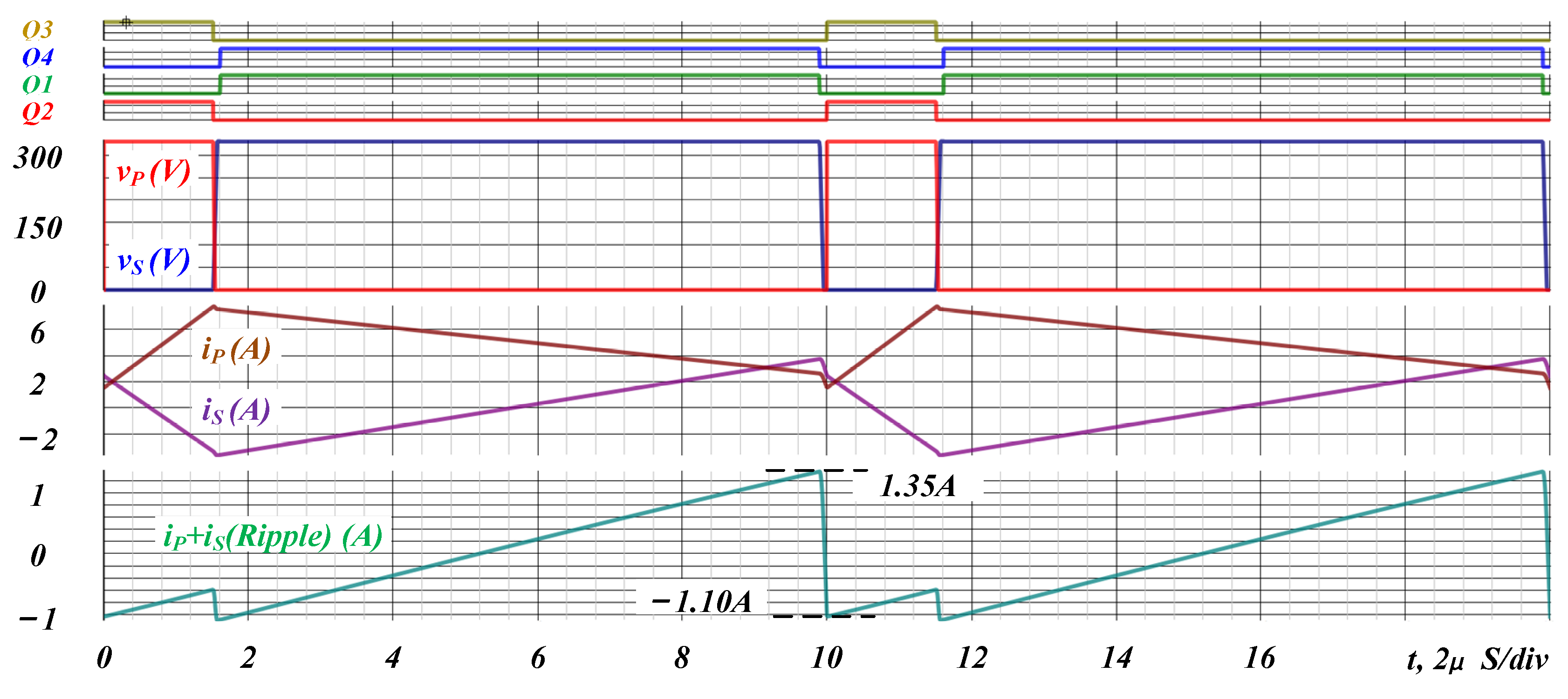
Figure 18 and
Figure 19 show the simulation results of the output current ripple of the stacked buck converter under the conventional dead time and low output ripple dead time modulation. The system architecture diagram and system parameters are shown in Figure 27 and
Table 1, respectively. Moreover,
RL = 10 Ω, and the dead time is set to 100 nS,
Te1 = 32.67 nS, and
Te2 = 20.34 nS.
Figure 18 and
Figure 19 show that with the conventional dead time simulation results, the peak-to-peak value of the output current ripple is 2.4 A and the RMS value of the current ripple is 745 mA. Given that simulation results of the low output ripple dead time modulation, the peak-to-peak output current ripple decreases to 443.53 mA, and the RMS value of the current ripple is 15.78 mA. Note that the dead time modulation method of the low ripple output can significantly reduce the amount of current ripple. The result is consistent with the theoretical analysis.
6. Small-Signal Model and Compensation Design
The small-signal model of the independent inductor cascaded buck converter has been proposed in the literature [
22]. Its small-signal model is extended to a coupled-inductor stacked buck converter, as shown in
Figure 20. In particular,
RSseq and
RSpeq are the total series resistance on the series path, and the resistance value is the sum of the on-resistance of the power switch and resistance of the inductor winding. Furthermore,
ESRCS and
ESRCP are the equivalent series resistances of the
CS and
CP capacitors, respectively.
To verify the accuracy of the small-signal model and determine the disturbance transfer function
Gdv of
duty to
vout under different load conditions, the circuit parameters are shown in
Table 1.
RL is substituted into 2.5 Meg Ω and 2.5 Ω. Using the actual circuit operation and small-signal model, we use the simulation software to run the individual
Gdv Bode diagrams, respectively
Gdv_circuit and
Gdv_model, as shown in
Figure 21. Moreover,
Figure 21 shows that
Gdv_circuit and
Gdv_model are consistent with each other, which proves the correctness of the small-signal model. Moreover, the worst case is when RL = 2.5 Meg Ω. Therefore, the compensator should be designed under the converter’s no-load condition. Given that
Gdv_circuit is consistent with
Gdv_model, the following articles will use
Gdv notation to represent the disturbance transfer function of duty to
vout, where
Gdv = Gdv_model = Gdv_circuit.
When considering the use of boundary limit control, the stacked buck converter’s small-signal model within the boundary-limited interval should be discussed. Given that the S-arm’s duty disturbance in the boundary-limited interval is 0, the small-signal model in the boundary control interval can ground the S-arm’s duty disturbance in
Figure 20. This result becomes the small-signal model of the stacked buck converter of the coupled inductance forms in the boundary limit interval. The model is shown in
Figure 22.
Substitute the
RL of
Figure 22 into 2.5 Meg Ω, plot the disturbance transfer function
Gdv_bd of duty to
vout in the boundary control interval, and place it in
Figure 23 together with the
Gdv in
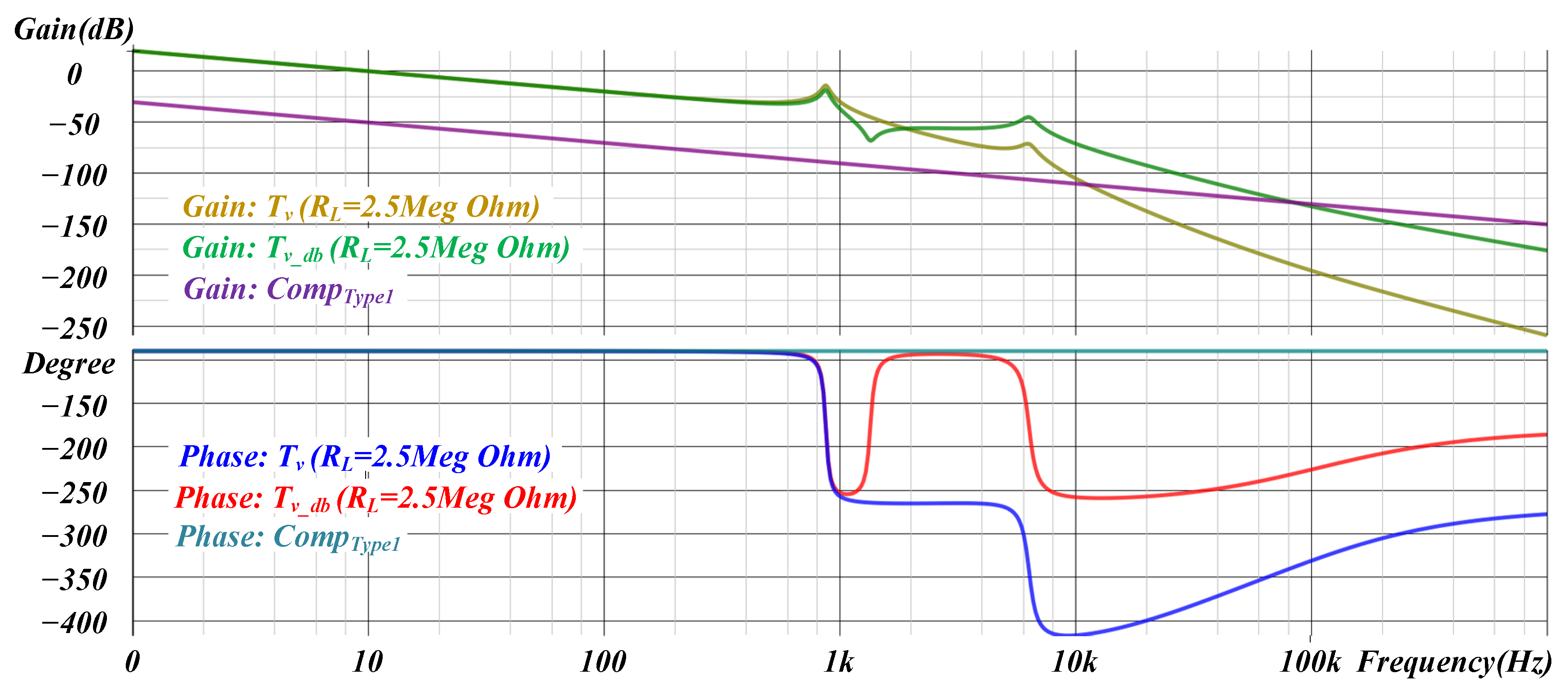
Figure 21 for comparison.
Figure 23 shows that the Bode plots of
Gdv and
Gdv_bd are extremely different regardless of the changes in gain and phase. Such characteristics will make it challenging to design the compensator with one compensator while satisfying the two closed loops’ high-frequency bandwidth and stability.
If the compensator’s design aims to satisfy
Gdv and
Gdv_bd, then the easiest method is to reduce the closed-loop bandwidth. Therefore, the first compensator example’s design parameters are shown in Equation (55), using single-pole compensation.
Figure 24 shows the closed-loop gain under the first type of compensator, where
Tv = GdvCompType1 and
Tv_db = Gdv_bdCompType1. Note that
Tv and
Tv_bd are stable and contain sufficient gain and phase margins. However, the closed-loop bandwidth is extremely narrow.
As the boundary control mode will eventually return to the ordinary operation mode, and
Gdv is used as the basis for the final system stability, the second type of compensator design concept aims to design only for
Gdv and disregard the stability of
Gdv_bd. The design parameters of the second type of compensator are shown in Equation (56).
Figure 25 shows the closed-loop gain using the second type of compensator, where
Tv = GdvCompType2 and
Tv_db = Gdv_bdCompType2. Note that only the closed-loop gain of
Gdv is stable, while the closed-loop gain of
Gdv_bd has insufficient GM and PM in two places. Although the closed-loop bandwidth of
Gdv is increased, the system has unstable factors in the boundary limit control mode.
Figure 26 compares the simulation results of the system transient response of the first and second compensators. The load resistance is switched from
RL = 2.5 Meg Ω to
RL = 2.5 Ω when
RL is t = 70 mS. When t = 120 mS, the load resistance is switched from
RL = 2.5 Ω to 2.5 Meg Ω again.
Figure 26 shows that the transient response of the first type of compensator is considerably slow, the boundary limit mode is not triggered, and the system is stable but takes a long time to reach the steady-state. However, the transient response of the second type of compensator has a short recovery time. It triggers the boundary limit mode. Hence, the performance of undershoot and overshoot is better, the output voltage is stabilized for a short time, and the system returns to stability in the general operation mode.
Figure 26 shows that with the second type of compensator, the system can eventually return to stability even though
Tv_db has unstable factors.


