1. Introduction
Power converters are electronic circuits whose aim is to adjust the output voltage to a desired fixed value (regulation task) or to a defined time-dependent function (tracking task). Power converters can be classified into step-down or step-up, depending on the output/input voltage ratio. The former (latter) takes an input voltage and outputs a lower (higher) value than the input. The boost converter is one the most prominent examples of a step-up architecture, mostly due to its simple design and high efficiency for unelevated values of the duty cycle [
1]. However, as the output/input ratio (gain) increases in the boost converter, its efficiency drops. This issue highlights the challenges in step-up converters in order to find highly-efficient designs with high gain capabilities. Solutions to this problem have been previously proposed [
2,
3,
4,
5], while using complex designs. These new designs involve an increased number of diodes, transistors, capacitors, and coils, which renders the analysis of these systems impractical. In many cases, the only techniques that are available for analyzing these systems are numerical simulations and averaged models. Unfortunately, those techniques can neither determine the behavior of the system in a wide operation range nor consider the effects of nonlinear phenomena.
The use of magnetically coupled inductors is one of the main ideas exploited so far in the design of highly efficient step-up converters (see [
6] for a list of applications). The boost-flyback converter that was proposed by [
7,
8,
9] is probably the simplest converter with high gain and high efficiency. It integrates two different converter topologies: boost and flyback, which operate with two magnetically coupled coils (see
Figure 1 for illustration). Despite the advantages of the boost-flyback converter, it was only analyzed in deep for the first time in [
10], while using an average model. Thereafter, the research devoted to the analysis and control of this power converter has increased [
11].
For instance, the boost-flyback converter under peak current-mode control was analyzed in [
12,
13] while using the complete discontinuous model. The authors took advantage of the piece-wise linear nature of the system, in order to utilize non-smooth stability assessment techniques [
14,
15,
16]. These works demonstrated the transition to chaos of a periodic orbit and the importance of the slope compensation. Other control design techniques include methodologies to compute the minimum value of the compensation ramp of the peak current-mode [
17], in order to enhance the stability region [
18] and control the system via the hysteresis band [
19]. These recently proposed methodologies emphasize the increasing importance of this power converter.
In this work, we propose applying a modified version of the Zero Average Dynamics (ZAD) control to the boost-flyback converter. The original ZAD strategy was first proposed in [
20]. The main idea behind the ZAD control is to force the error of the system and its derivative to evolve as dynamical variables with zero average. To do this, the duty cycle is computed in such a way that the average condition is satisfied. In [
20], a piece-wise linear approximation of the error function was proposed and successfully used in [
21,
22,
23,
24] due to the complexity to solve the equation to find the duty cycle. Unfortunately, the ZAD controller is much less robust than a regular sliding control. For this reason, here we propose controlling the system while using the same idea, i.e., we build a function
s that depends on the state of the system. However, as the boost-flyback is a much more complex system, we include several considerations. Firstly, we do not consider the derivative part of the error in order to avoid noise amplification in practical applications. Secondly, we include an integral control action which adds robustness to the system. Finally, we incorporate information of the currents flowing through the coils to the function
s. Other considerations that are related to the behavior of the surface and its slopes remain unaltered. This modified ZAD controller is here named Zero Average Surface (ZAS) control.
The paper is organized, as follows: in
Section 2, we show the mathematical model that describes the dynamics of the boost-flyback converter. Next, in
Section 3, we describe the details of the ZAS control strategy when applied to the boost-flyback converter. Additionally, we show a simplified way to calculate the duty cycle by making use of the typical topological sequences that form the stable orbits in the converter. In
Section 4, we analyze the stability of the orbits that result from the application of the control strategy. We perform the stability analysis under the variation of several parameters, using bifurcation diagrams and Floquet multipliers. Furthermore, in
Section 5, we show the controlled system’s response to a variety of disturbances, showing that the converter performs satisfactorily, despite the scale of the disturbances. Finally, in
Section 6, we present some concluding remarks and point out some open problems.
2. Dynamics of the Boost-Flyback Converter
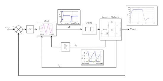
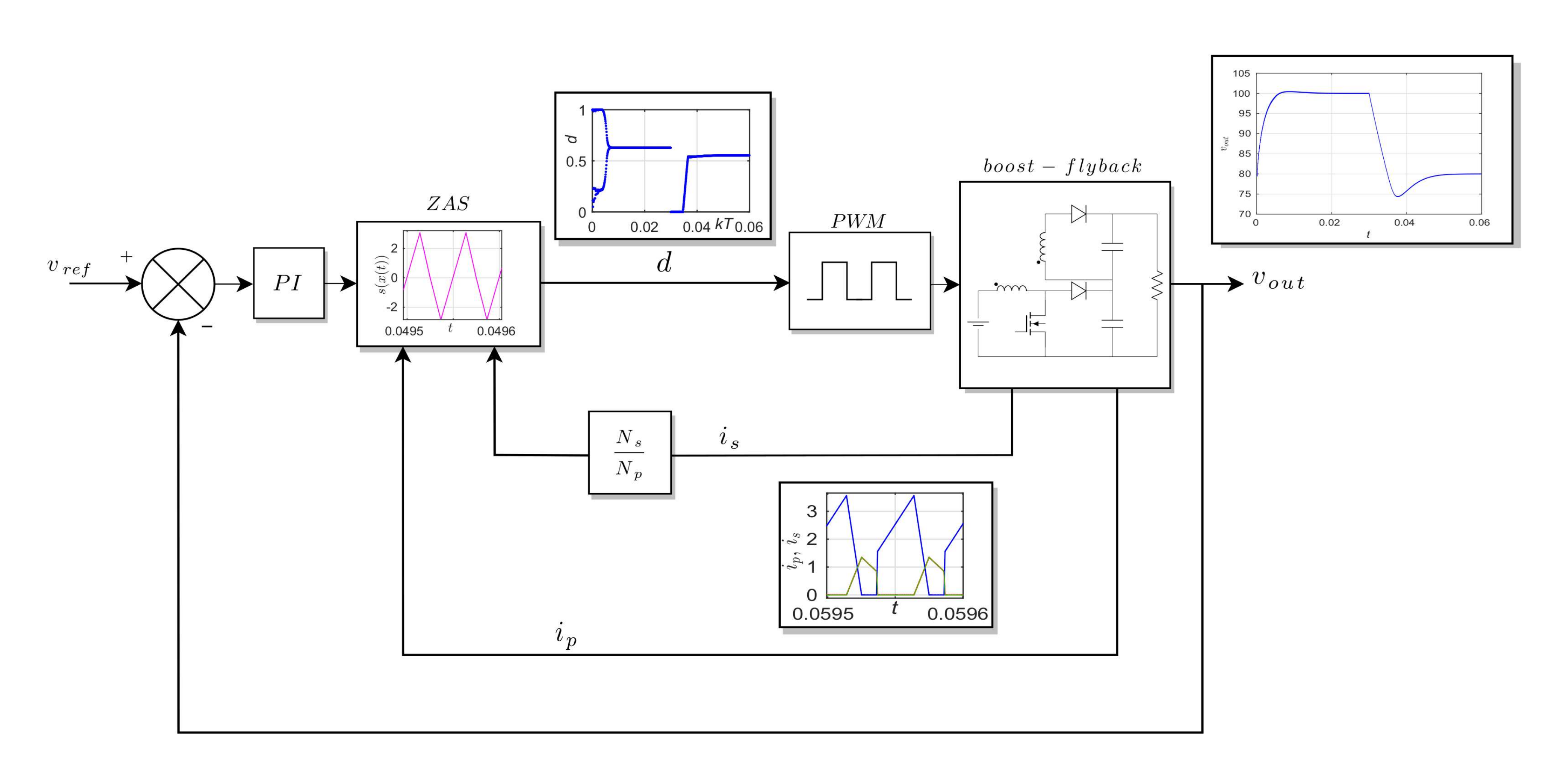
Figure 1 illustrates the diagram of the boost-flyback converter together with the ZAS control module. A boost-flyback converter is composed by two capacitors
and
, two magnetically coupled coils
(primary) and
(secondary) with their respective internal resistances
and
. Additionally, the system has a MOSFET
acting as a switch with an internal resistance
and two diodes (
and
). The input is provided by
and the output
is the sum of the voltages across capacitors (
). The state of the system is then given by the voltages across the capacitors
and
, the currents flowing through the coils
and
, and the integral of the output error
e. The error is, in turn, defined as the difference between the real output and the desired one, i.e.,
. Altogether, the state space
is formed by the variables
with
.
The state of the diodes and the switch can only take values in the discrete set , i.e., each one of them can only be in an open position (no current flowing) or closed position (current is allowed to flow). Additionally, the transition between open and closed states is assumed to be instantaneous. The presence of nonlinear elements (diodes and switch) transforms the system into a non-smooth system that can be described through a set of differential equations that changes as the positions of the switch and diodes change.
Combining the different states of the diodes and the switch, there are eight topologies. However, only six of these are physically viable, which are reported in
Table 1. The primary coil (
) and secondary one (
) interact with each other through the mutual inductance
, with
being the coupling coefficient. Additionally, we assume a small internal resistance
for the switch, when it is active. When the diodes are closed, the current flow is positive and their terminal voltage is zero (ideal diodes). Conversely, when diodes are open, the terminal voltage is either negative or zero, which means that the current flow is null. In addition to the differential equations for each topology, the dynamics of the system are completed with a set of algebraic restrictions of the state variables
x. For more details of the boost-flyback converter, we refer the reader to [
10,
12,
13]. Finally,
Table 1 summarizes the equations that describe the converter at each admissible topologies.
In
Table 1,
. In short hand notation, the system can be expressed as:
where the subscript
runs through the different vector fields that are specified in
Table 1 and variables are assigned as
,
,
,
and
. Notice that the states
,
,
, and
can only be present when the MOSFET is inactive (OFF), and states
and
when the MOSFET is active (ON).
3. Zero Average Surface Control Technique
Pulse Width Modulation (PWM) is a widely used methodology for controlling the output voltage in a power converter [
25]. In a PWM, the MOSFET commutes between the OFF position (
) and the ON position (
) in order to regulate the system’s output. For the boost-flyback converter, the more time the discrete signal remains in the ON position, the higher output voltage. In order to obtain the desired output voltage value, it is necessary to compute the duty cycle (
d), i.e., the ratio between the time that the signal
and period
T of the MOSFET, namely
. In summary, the duty cyle is the key quantity that one needs to control in a PWM based power converter. In this section, we present a simple methodology to calculate
d at each switching cycle, called Zero Average Surface control.
3.1. Defining the Surface
Briefly speaking, we calculate the duty cycle based on the idea that a certain state-dependent function
has a zero average in a PWM cycle. The function should include the most information regarding the system’s state. This idea is inspired by a previously reported technique, named the Zero Average Dynamics (ZAD) strategy, which was originally applied to the buck power converter [
20,
26]. In these works, the function
was defined as a linear combination between the output error and its derivative. However, the absence of an integral control rendered the robustness of the system unsatisfactory. In this work, we define the function
via a strategically selected combination between the five states of the boost-flyback: The voltages across the capacitors are linked through the desired output voltage. Additionally, the currents through the coils are linked via the magnetization current. Finally, an integral control action is also added, such that the function reads
Because
supplies the desired output voltage
(see
Figure 1), then
is a proportional control action. Furthermore, the integral control is
, where
. These two terms define a PI controller that reduces the steady state output error and handles the transient state when the system is subject to disturbances and/or changes in the system’s parameters. The current values
and
, enter into the expression via the magnetization current
[
27], where
(
) is the number of turns in the primary (secondary) coil. This last ingredient of the expression acts as an additional proportional control and its role is regulated with
.
3.2. Piece-Wise Linear Approximation of the Function
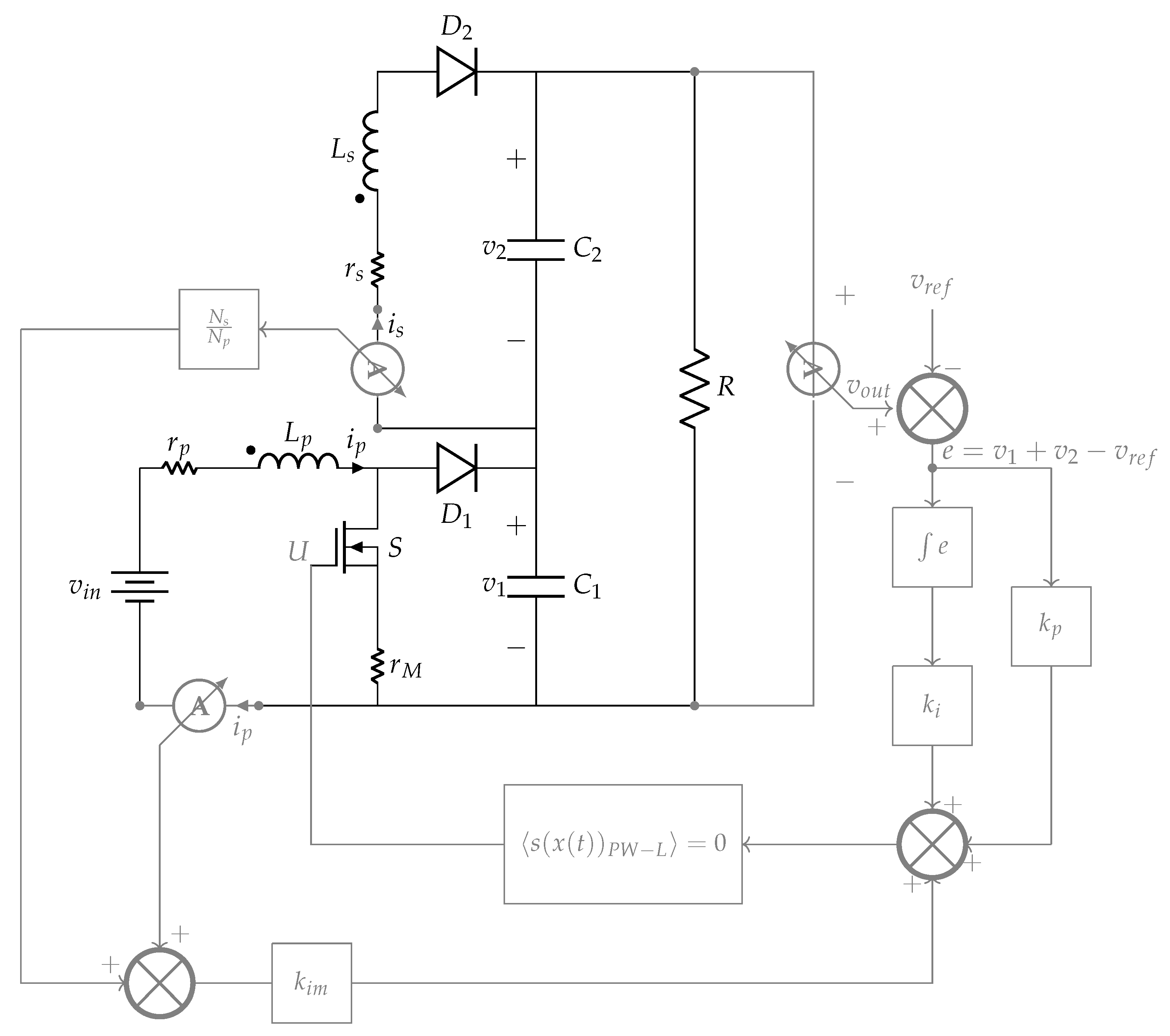
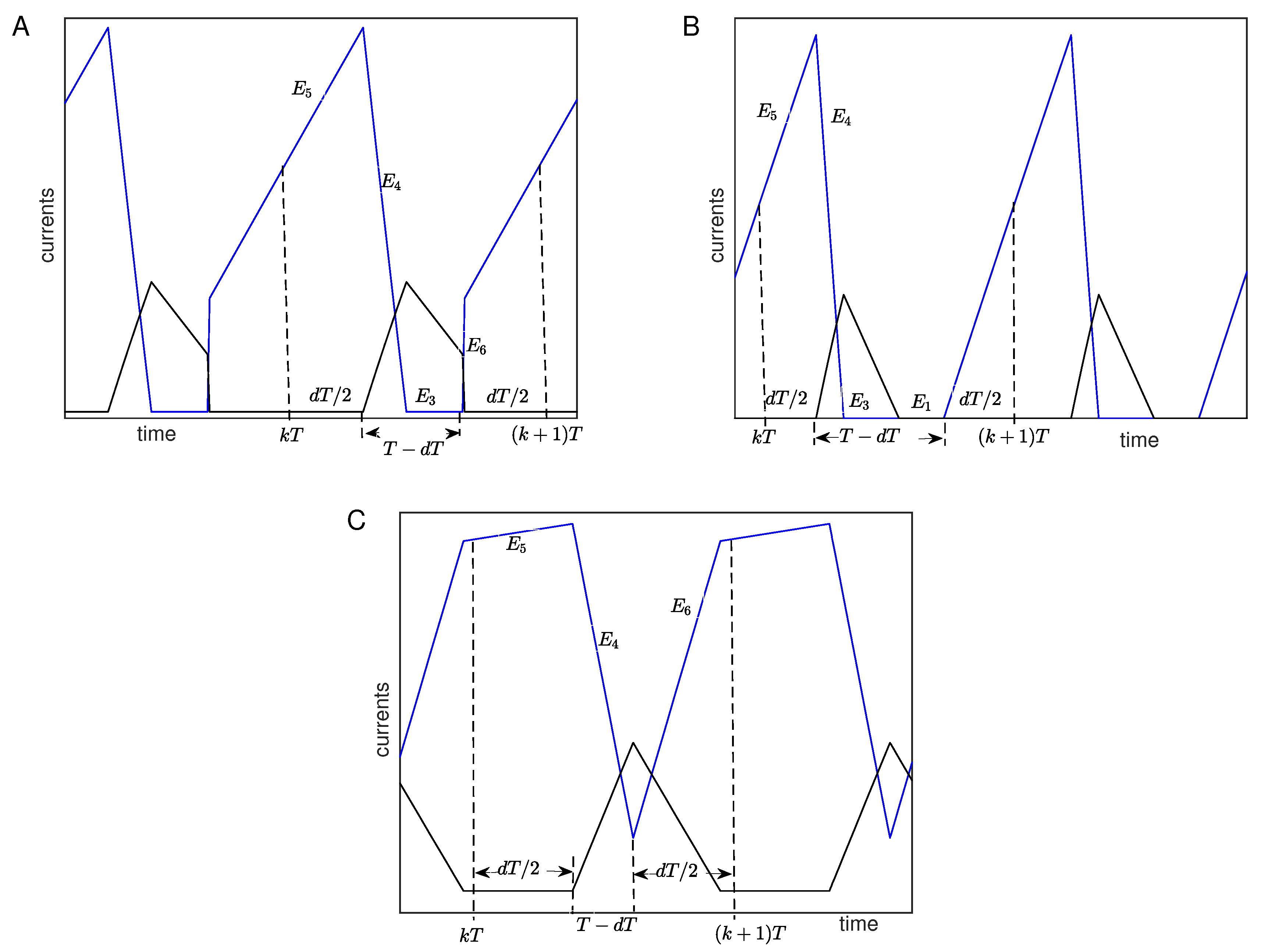
The control signal
u in a centered PWM (see upper part of
Figure 2) can be defined as:
where
μs is the sampling period and
is the duty cycle. As previously mentioned, the aim of the controller is to compute the duty cycle
d in order to achieve, in every
T-cycle, a zero average of the function that is defined by (
2), i.e.,
In this work, a centered PWM is used to compute the duty cycle in every
T-cycle, such that Equation (
4) meets the zero average criterion. Equation (
4) can be written as:
Solving this equation implies computing the zeros of a complicated transcendental equation, which is highly inefficient from a practical point of view. In order to overcome this problem, we assume that the surface
can be approximated via a piece-wise linear function in time
, forming a triangle-like wave (see lower part of
Figure 2). Secondly, we will assume that the derivatives of the first and third segments of
are equal, and, thirdly, we suppose that we can calculate the slopes of the piece-wise linearly approximated function at the beginning of the cycle (denoted as
). In summary,
can be expressed as:
Here,
and
are the offset values of the three segments (see
Figure 2). Similarly,
and
are the slopes that are computed from the expression of
while using the state values at the beginning of the cycle. These derivatives can be written in the following form:
where the subscript
i can take the values
, when considering that
and
are the two admissible topologies with MOSFET in active mode. Similarly, the subscript
j can take the values
, which is consistent with the fact that the admissible states with the MOSFET in inactive mode are
,
,
, and
. In the following section, we will describe the topologies that are to be used to compute
and
.
3.3. Computing the Duty Cycle
A lot of analytical and numerical results [
10,
12,
13,
17,
18,
19] have shown that there are three topological sequences that form different period-1 orbits, depending on the system’s parameters: (i)
, (ii)
, and (iii)
.
Figure 3 shows the three basic possible period-1 orbits and their topologies. According to these orbits, we can draw the following conclusions: (1) out of the topologies appearing with the MOSFET in active mode (
and
),
is always present. Similarly, for topologies with the MOSFET in the inactive state (
,
, and
)
is always present. (2) The power converter always switches the MOSFET position between states
and
. These two facts lead us to conclude that the main part of the sequence that describes any periodic orbit is
. Subsequently, to apply the approximation (
6), and taking into account Equation (
7), we can describe any sequence as
, followed by
. This implies that
is computed with topology
and
is computed with topology
. Under this consideration, the orbits that the system can exhibit are
(5436 for short, see
Figure 3A),
(5431, see
Figure 3B), and
(546, see
Figure 3C).
Particularly, in every cycle, we will assume that is present for a time , and, at , the system commutes to . Moreover, when the MOSFET is inactive, i.e during the interval , the system may undergo one or two secondary transitions: (i) the first one will appear when , and, in this case topology, guides the system and (ii) the second one will appear when and guide the dynamics. Finally, for the interval , the system will switch its dynamics to in the cases in which and it will rapidly evolve towards 0, where the topology leads the dynamics of the system. Conversely, when the previous topology in inactive state was in , it will immediately switch its behavior to .
According to the previous considerations,
must be evaluated with
and
must be evaluated with
. Additionally, the offset of each one of the segments can be computed as:
and
where
is the value of the
at the beginning of the cycle. With these assumptions, Equation (
5) is simplified in such a way that an algebraic equation is solved instead of a transcendental one. The simplified equation now reads as:
After some straightforward algebra, the duty cycle
d can be solved as:
Finally, because the duty cycle
to apply at the
-cycle must be bounded within the range
, we complement the duty cycle calculation with the following saturating conditions:
Altogether, the design of the proposed controller can be summarized, as follows:
Define a sampling time T of the MOSFET according to design requirements.
Define the surface
, including the information of: (i) the states of the system and (ii) the integral of error to correct steady state error (Equation (
2)).
Apply the piece-wise linear approximation
of the surface (Equation (
6)).
Sense the output voltage error, magnetization current, and integral of error at the beginning of every cycle.
Compute, at the beginning of every cycle, the duty cycle that ensures
(Equation (
9)).
Apply the computed duty cycle (Equations (
10) and (
11)).
3.4. Stability Analysis of the Period-1 Orbits
With the aim of assessing the stability of the period-1 orbits, we proceed to calculate the associated Floquet multipliers
. Floquet multipliers are the eigenvalues of the monodromy matrix
, which describes the evolution of an infinitesimal perturbation
around the target periodic orbit from one period to another, namely
In the case of smooth systems, computing
can be done straightforwardly via the linearization of the vector field. Conversely, the formal calculation of monodromy matrices in non-smooth systems requires appropriate corrections that are induced by the transitions between topologies, which are described by saltation matrices [
28,
29]. Here, we will make use of a much simpler numerical approach to the calculation of
, which only requires the evolution of a reasonable number of perturbed orbits between two periods. Because our system is non-autonomous, the periodic orbit is stable if all eigenvalues lie within the unit circle [
30]. The algorithm can be summarized as (see [
31] for details):
Find the periodic orbit and the associated duty cycle d, which guarantees that and identify the topological sequence that fulfils the condition.
Create N randomly perturbed orbits with .
Evolve the perturbed orbits over a period T, such that .
Store the differences of every state between the perturbed and the unperturbed orbits at the beginning of the period () and at the end of it ().
Approximate the monodromy matrix as:
Compute the Floquet multipliers via the eigenvalues of .
4. Numerical Results
We proceed to set the values of the constants
,
, and
in order to guarantee the stability of the orbit. It can be seen that the controller includes two loops: the first one is external and it corresponds to the voltage control loop, which is formed by the control action that is based on the error and its integral. This loop guarantees that the output voltage follows the reference value. For this reason,
should be high in order to obtain a fast dynamic response. Conversely, as the proportional action controlled by
is more sensitive to errors, it should not be high in order to avoid instabilities. The second loop, corresponding to the proportional control of the magnetization current, is an inner loop, and it provides stability to the system, and, following the same guidelines as before, it should not have a high value. For simulations, we set the constant values
and
close to the values that were reported in [
12,
13]. In turn,
has been set, such that a stable period-1 orbit with topological sequence 5436 is obtained, which we have selected as the target periodic orbit.
In what follows, we investigate the stability of the period-1 orbit that was described by the sequence 5436 using bifurcation diagrams and Floquet multipliers. Several works have demonstrated that this orbit is very stable [
12,
17,
18,
19]. In this section, only the variation of the parameters
R,
, and
are analyzed, such that
,
, and
remain fixed. In
Table 2, all of the parameter values are presented. The nominal values of
R,
, and
are identified with the subscript
N and the range of variation used in the stability analysis is shown in front.
Let us start by analyzing the behavior of the system under variations in the input voltage
. In
Figure 4, two different protocols are presented. The red continuous curve corresponds to increasing variations of the parameter, while the blue empty symbols refer to decreasing variations of the parameter. On the one hand,
Figure 4A shows that, by increasing
, a period-2 orbit shows up as signaled by the presence of two values of the duty cycle. This 2-periodic orbit is characterized by one saturated cycle, which remains stable for almost the whole range of the parameter variation until it suddenly transforms into a period-1 solution at
V. Interestingly, the same analysis performed starting with a high value of
reveals the co-existence of a stable period-1 orbit with the saturated solution that was described before. The period-1 solution remains stable until
, where it bifurcates to an unsaturated period-2 orbit, which eventually merges at
with the saturated period-2 orbit found for increasing
. The period-1 orbit corresponds to the topological sequence 5436 and
Figure 4B depicts the norm of largest eigenvalue
of the monodromy matrix that is associated with this orbit (filled black symbols). By looking at
, one can see that the stability is lost (
) at
, i.e, at the bifurcation point. It shall be noticed that, at smaller values of
, there indeed exists a period-1 orbit that is nonetheless unstable (empty symbols). It is worth noticing that the region in which stability of the desired orbit is lost (small
) corresponds to high gains of the converter. In this scenario, the current requirements are high in the primary coil. This observation helps to understand the mechanism of the bifurcation: as the duty cycle increases, the current flowing through the primary coil increases. Therefore, when the switch is turned OFF and topology
kicks in,
cannot evolve towards 0 before turning the switch ON again. The consequence is that topology
is never reached and the orbit evolves as 546 during one cycle (upper branch of the unsaturated period-2 orbit). In the next cycle, the 5436 is recovered, because the initial condition of the primary current is now at a much lower value, allowing for
to reach zero value when the MOSFET is OFF. Finally, the upper branch eventually saturates to
, which indicates that, during one whole period, the system remains in topology
. Meanwhile, in the next cycle, the sequence 5436 is recovered.
Figure 4C depicts the output error that is produced by the coexisting orbits previously described. Here, one can see that the output error in the two sampled points of the period-2 orbits are quite similar, producing the thick lower line. Similarly, the error that is associated to the period 1 orbit, while it has a larger absolute value, remains within the reasonable range <0.25%.
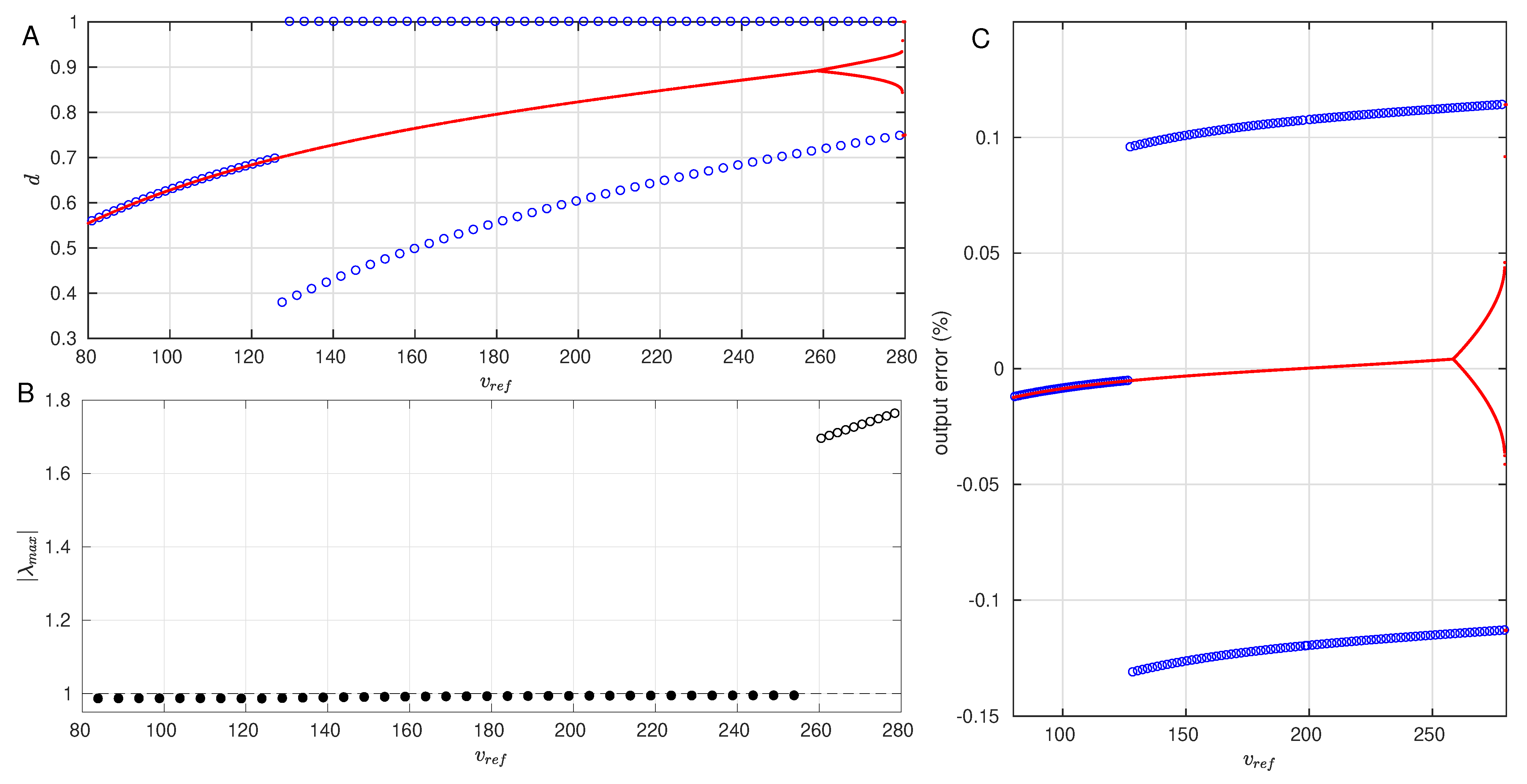
Next, we focused our attention on the bifurcations that arise by varying the reference voltage
with the same protocols described before. In
Figure 5A, we show the values of the solution of the duty cycle by increasing (red) and decreasing (blue) the reference voltage
. Following the increasing bifurcation curve, it is possible to see that the period-1 orbit 5436 is stable over a large range of
. After this point, the orbit bifurcates to the unsaturated period-2 orbit until it finally reaches the saturated period-2 orbit. As described in
variation, the bifurcation mechanism is the same: the bifurcation is produced by the high
requirements, which leads to increasing values of the duty cycle.
Figure 5B supports these findings, i.e, the norm of the largest Floquet exponent of the period-1 orbit is
over the same range of stability that is reported above. Once again, after the bifurcation point, a period-1 orbit still exists with unstable nature.
Following the decreasing parameter protocol, one starts with the saturated 2-period cycle, which persists until V, indicating a bistable behavior in that interval. Below this value, the saturated period-2 orbit disappears and the only attractor is the period-1 cycle.
Additionally,
Figure 5C displays the output error using the increasing and decreasing protocols, where it can be noticed that the period-1 orbit presents an almost negligible error (<0.02%) that rapidly increases after the bifurcation. Nevertheless, even the period-2 orbits (saturated and unsaturated) are associated with reasonably small values of the error (<0.2%).
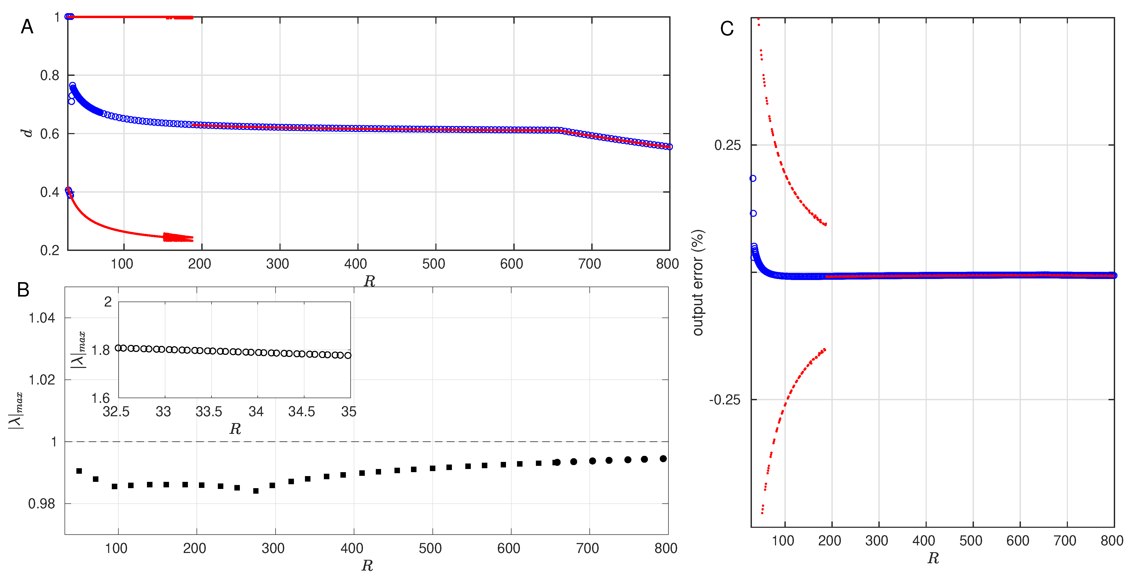
Finally we will focus our attention on the bifurcations with varying load (
R), as displayed in
Figure 6. It is useful to start with the decreasing protocol, where a period-1 solution is present in the interval
. This periodic solution corresponds to the topological sequence 5431. This orbit is different from the orbit 5436 that we have studied so far. This sequence appears when the duty cycle is small and, therefore, the MOSFET remains in the OFF position for a long time. During this OFF time, the current through the secondary coil
has enough time to reach a zero value. This means that topology
guides the dynamics for the rest of the OFF interval. Once the switch is active again, topology
immediately kicks in without the intermediate topology
. The stability of the 5431 orbit is corroborated with the values of
in the same interval (solid circles in
Figure 6B). At
, the usual 5436 orbit is recovered as the duty cycle increases. The orbit remains stable until a rapid bifurcation to the period-2 solution at
and the subsequent saturation. This can be also observed by the stable interval that is characterized by
of the 5436 orbit (solid squares) in
Figure 6B. As expected, it changes stability (
) at the bifurcation point (empty circles).
Similarly, by increasing
R, one starts with the saturated period-2 orbit. It remains stable until
, where a chaotic attractor emerges in a small window. This attractor disappears and gives rise to the stable period-1 sequence 5436 at
. As in the previous cases, the associated errors of the period 1 orbit are small, as illustrated in
Figure 6C, and it only starts increasing at the bifurcations. Despite this, the period-2 orbits also display small values of the error.
5. Disturbances Rejection
So far we have shown the co-existence of the desired period-1 orbit with a period-2 solution over a large interval of the studied parameters. In this section, we test the robustness of the orbit 5436 when different disturbances are present in the system. The disturbances that are simulated in this part correspond to abrupt changes in the parameter values, which were used as bifurcation parameters.
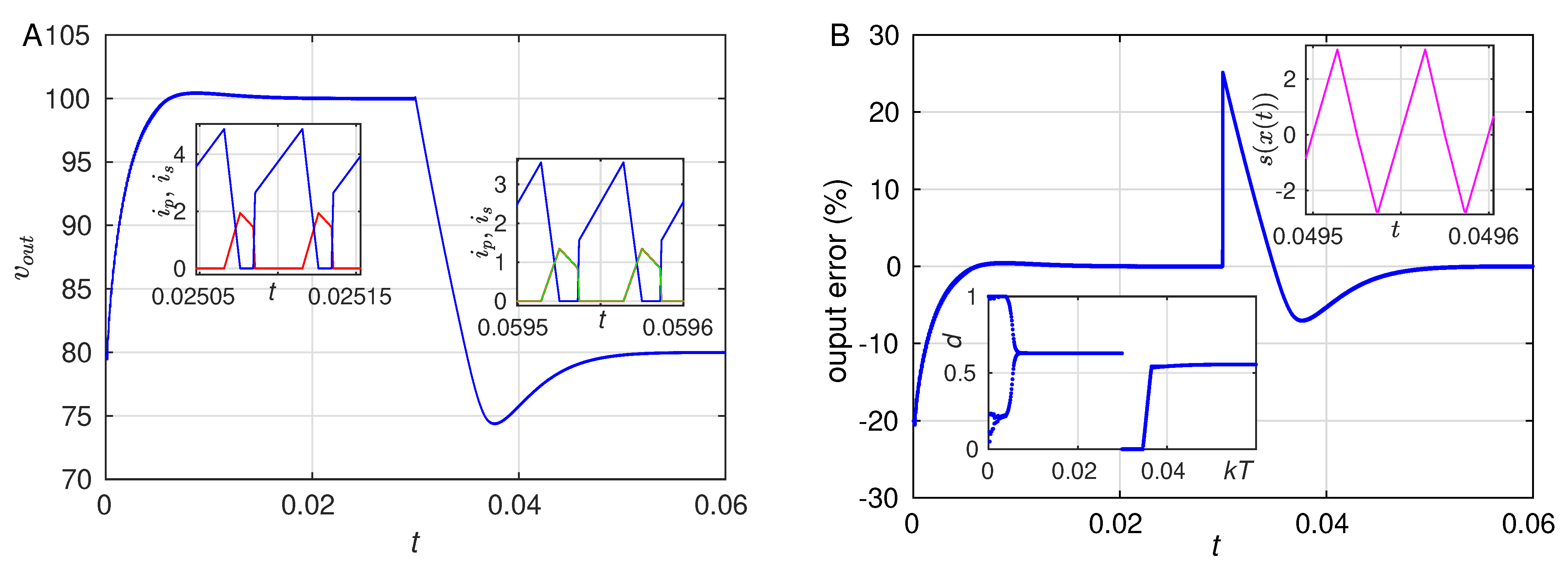
Firstly, in
Figure 7A, we show the convergence of the system’s output from an initial value of 80 V to a desired value of
V. It can be seen that the system rapidly establishes to the steady state value in around
ms. After this, a sudden change in the desired output from
V to
V is performed at
ms and the system is able to reach the new desired value at around
ms. In
Figure 7B, we show the evolution of the output error to the disturbances that were described before, together with the evolution of the duty cycle and a sample trace of the function
in a small time interval. In the case of the desired period 1 orbit, the duty cycle transiently saturates, but it eventually reaches the asymptotic
d-value corresponding to the stable orbit (see insets). Moreover, one can also notice that the piece-wise linear assumption of
in Equation (
6) is adequate, as testified by the virtually piece-wise linear nature of the function that is defined in Equation (
2).
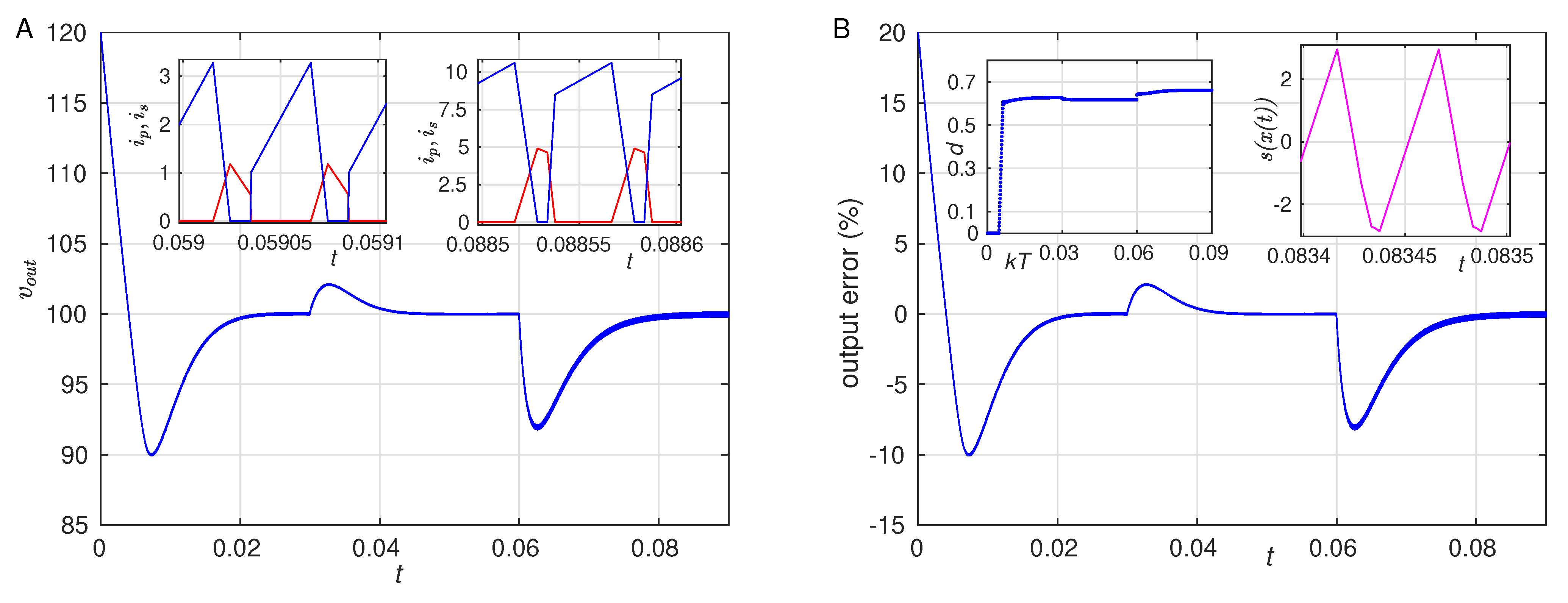
Now, we analyze the behavior of the system when the disturbance is applied to the load. At
ms, the resistance
R changes from 200
to 350
and it is forced to change again at
ms to 80
. The results of this numerical experiment are depicted in
Figure 8. As before, the system is able to handle the disturbances and it reaches the desired value of the output voltage in
ms, depending on the size of the disturbance. A close look to the function
in the upper inset of
Figure 8B reveals the effect of the secondary transitions within the same position of the MOSFET in the shape of
. Here, one can see the appearance of a further linear segment, which, nevertheless, does not substantially affect the three-segment piece-wise linear approximation used here. This can be testified by the small errors that are reported in the main panel shown in
Figure 8B.
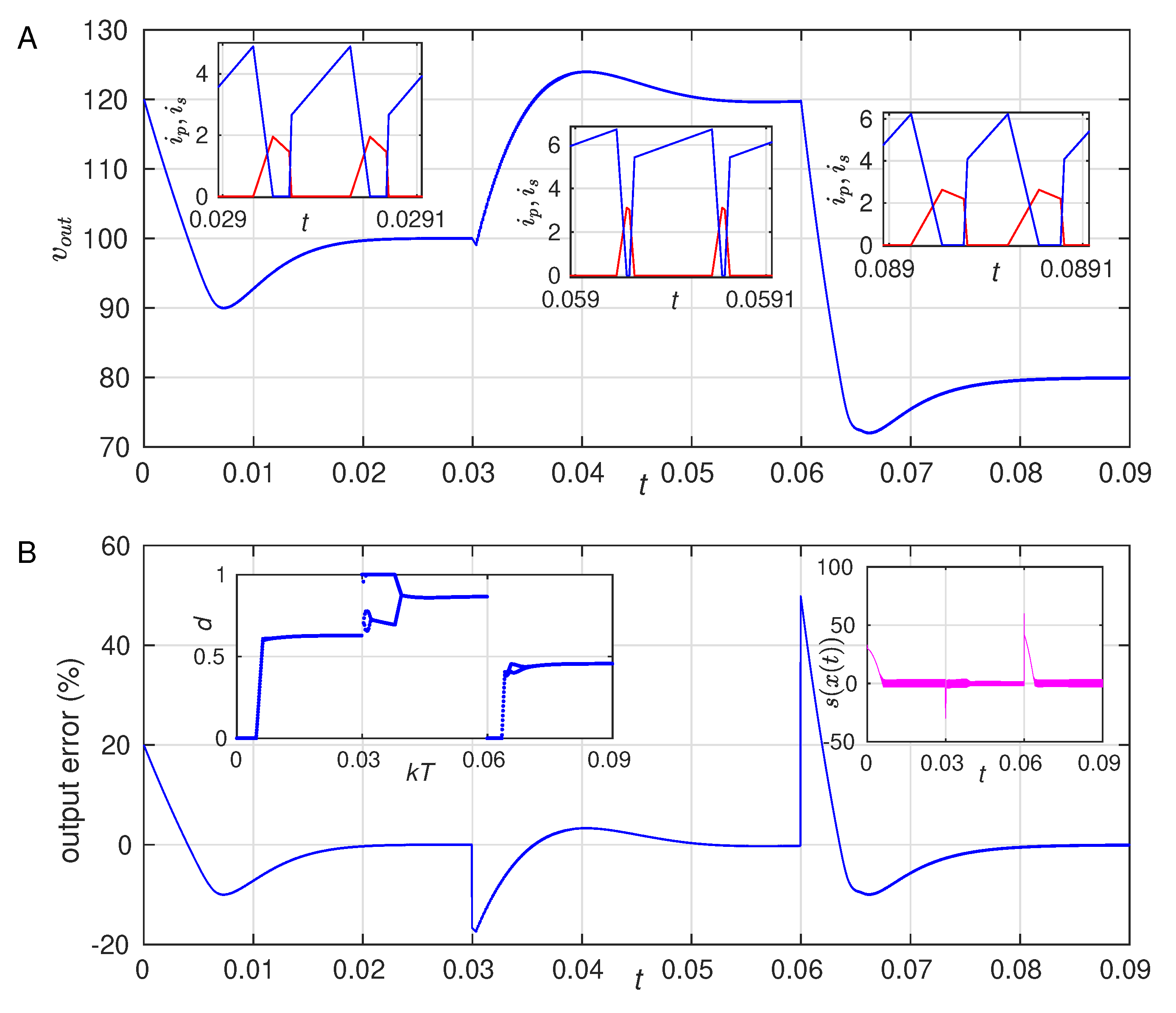
Finally, the last disturbance involves, simultaneously, changes in the reference value, load resistances as well as in the input voltage. Firstly, at
ms,
changes to 120 V,
R changes to 350
and
= 8 V. Secondly, at
ms, the reference voltage changes to
= 80 V, the input voltage changes to
V, and the load changes to
.
Figure 9 shows the results of this experiment. In this figure, it is possible to see that, despite the sudden transitions in a large proportion of the system’s parameters, it evolves satisfactorily to the desired orbit. For the sake of visualization, we have included the whole time series of the function
in order to show that it has indeed a zero-average behavior in steady state, as hypothesized by the ZAS strategy.
From the numerical experiments of this section, we can assert that the basin of attraction of the period-2 solution is small when compared with the basin of the period-1 orbit. This can be inferred, because, according to the bifurcation diagrams described in
Section 4, the period-2 solution should be present in the different disturbances applied here; however, the solution always evolved towards the desired period-1 solution.
6. Conclusions and Future Work
In this work, we have successfully applied the Zero Average Surface (ZAS) controller for output regulation in a boost-flyback converter. The strategy consisted of the definition of a state-dependent function—
—with the most information of the system’s state. The ZAD control technique (precursor of the ZAS strategy presented here) was originally used to force a function that depends on the error and its derivative to have a zero-average in a PWM cycle [
20,
21]. Here, we have shown that adding an integral control action and imposing in every cycle a zero-average of a strategically chosen combination of the states, renders the system quite robust over a wide interval of input voltage, reference voltage, and load. Moreover, the original ZAD has been used to control bilinear systems [
21,
22,
23,
24,
32], where the system is only represented by two topologies. Nevertheless, when the converter has a more complex topology, as in the case of the boost-flyback converter, the computation of the duty cycle gets more difficult. In contrast, with the ZAS technique, we have been able to obtain a simple algebraic expression of the duty cycle while using few approximations of the converter’s dynamics and the state of the system at the beginning of the cycle. The duty cycle expression can be easily implemented on an embedded hardware system in order to generate a PWM signal, where the state variables are only sensed at the beginning of the switching period.
One of the main advantages of the ZAS controller is that it is designed to operate at a fixed frequency (the inverse of the sampling period T). Other controllers that make use of a variable frequency introduce undesired frequency-dependent harmonics to the signal. Eliminating such harmonics require the addition of different filters that add to the complexity of the overall system. Moreover, variable frequency techniques require semiconductor devices that fit within the ranges of commutation frequencies in order to guarantee a correct operation. For these reasons, the ZAS controller is a desirable strategy when the harmonics of the output signal are undesired.
Despite the fact that the function provides information of all five states of the system, it only relies on the tuning of three parameters (two for the proportional terms and one for the integral term). These can be further reduced to two parameters by means of a properly selected normalization of the parameters. Nonetheless, we have chosen, during the development of this work, to write all of the parameters down explicitly to keep track of the individual contributions of the terms in the function .
Even though the boost-flyback exhibits three different stable period-1 orbits, we have seen that the orbit 5436 was consistently the most robust across the experiments. Additionally, we reported that the stability of the orbit was lost by means of a period doubling and a subsequent saturation of the duty cycle at high values of the converter’s gain. In our numerical experiments with varying and , the value of the gain at which the bifurcation occurred was quite similar, namely . This seems to suggest that the boost-flyback converter controlled via the ZAS strategy is adequate for intermediate output voltage gains, and different controllers should be used for higher gains.
We showed that the robustness of the 5436 orbit is related with the larger region of attraction in the state space (basin of attraction) when compared with other coexisting attractors. This is consistent with previously reported results (see [
12,
13,
17,
19]). The calculation of the precise size of the basin of attraction is not an easy task, and it usually involves the application of the so-called Lyapunov direct methods, which are hard to apply, especially in non-smooth systems. In the case in which a single attractor is found, it is also non-trivial to determine whether this attractor is either globally or locally stable. Recent techniques that are based on contraction theory [
33] allow for assessing global stability, even in non-smooth systems [
34,
35], including power converters [
36]. Similar approaches could be applied to the boost-flyback converter in future research.
In the bifurcation diagrams varying the load, we suggested the presence of a chaotic attractor in a small window of the diagram. This result, together with other preliminary experiments—not shown here—performed at very low values of the parameters bring to light the need of a more complete characterization of the system. Such characterization must be performed, not only in terms of Floquet multipliers, but also Lyapunov Exponents as a preliminary step before an experimental implementation. This is part of an ongoing work that presents some challenges itself: For instance, the (formal) calculation of the Floquet multipliers and Lyapunov exponents require the use of the saltation matrix formalism for the correction of the linearised evolution of the system (perturbation’s dynamics), due to the discontinuities in the vector fields [
28,
29]. While this problem is relatively easy to solve in the cases in which the switching from one vector field to another is defined by a precise value of the state at the time of the discontinuity, we are here approximating the time of the discontinuity as a function of the states in the previous cycle. This calls for the need of a different approach to assess linear stability, for example, via the direct linearisation of the event driven map, which has been successfully used in applications involving pulse coupled oscillators [
37,
38].
In summary, the ZAS technique is ideal for applications that require: (i) intermediate gains, (ii) large operation region, and (iii) disturbance rejection. Examples of devices that required these specifications include hybrid electric vehicles [
39,
40], voltage balancing [
41], photovoltaic panels [
42], LED technologies [
43], and correction of the power factor [
44]. Finally, with the aim of contextualizing the contribution of this work, we present, in
Table 3, a summary of the advantages and disadvantages of different controllers that have been applied to the boost-flyback, and how they compare with the ZAS technique that was used here.


