Abstract
In this study, an optimization procedure was proposed for the magnetic component of an integrated transformer applied in a center-tap phase-shifted full-bridge converter. To accommodate high power–density 0demand, a transformer and an output inductor were integrated into a magnetic component to reduce the volume of the magnetic material and the primary and secondary windings of the transformer were wound on the magnetic legs to reduce conduction loss attributable to the alternating-current resistor. With a focus on the integrated transformer applied in a phase-shifted full-bridge converter, circuit operation in each time interval was analyzed, and a design procedure was established for the integrated magnetic component. In addition, the manner in which output inductance was affected by the mutual inductance between the transformer and the output inductor in the integrated transformer during various operation intervals was discussed and, to minimize circuit loss, a design optimization procedure for the magnetic core was proposed. Finally, the integrated transformer was applied in a phase-shifted full-bridge converter to achieve an input voltage of 400 V, an output voltage of 12 V, output power of 1.7 kW, an output frequency of 80 kHz, and a maximum conversion efficiency of 96.7%.
1. Introduction
Rapid technological advancements have greatly increased the demand for cloud servers, which calculate and store data, increasing the demand for electricity. To accommodate converter design requirements for reduced loss and volume, improving the efficiency of electric power conversion and increasing power density have become prominent considerations in current technological development. Most power supplies for servers adopt a two-stage circuit topology. The first stage comprises power factor correction equipment for conversion from alternating current (AC) to direct current (DC) and the second stage an isolated DC–DC converter with high-voltage DC as the input and low-voltage DC the output.
The typical types of isolated converters used in server power supplies are phase-shifted full-bridge converters and resonant converters. LLC resonant converters [1,2,3] achieve wide-range zero-voltage switching (ZVS) on the primary side and ZVS on the secondary side and are thus suitable for application in high-wattage and high-frequency devices. The disadvantage of LLC resonant converters is the absence of output inductors at the output end. Therefore, when used in low-voltage high-current devices, LLC resonant converters require more capacitors connected in series to meet output voltage ripple specifications.
For a phase-shifted full-bridge converter [4,5,6,7,8], the switch on the primary side does not achieve full-range ZVS, and the synchronous rectifier on the secondary side exhibits high switch stress. However, the converter structure features an output inductor, which reduces the number of output capacitors. In addition, the ZVS on the primary side of the converter and switching current that exhibits an approximately square wave on the secondary side effectively reduce the primary and secondary-side currents; this reduces the switch conduction loss and thus facilitates high efficiency for applications in high-wattage devices. When this structure is used in devices with a high-current output, a center-tap or current-doubler rectifier is typically adopted for rectification on the secondary side of a transformer. Compared with a center-tap structure, a current-doubler structure reduces the conduction loss in the secondary winding of a transformer by half. In a circuit, a magnetic component comprises a transformer and two output inductors, which increases the volume of the circuit. As the number of magnetic components increases, the number of joints in the circuit design also increases; therefore, when a large current is present, integration between windings and circuit components reduces the conduction loss and contact loss.
Relevant literature features the use of integrated magnetic components to integrate transformers and output inductors into one magnetic component, thereby reducing the number of magnetic components in a circuit and improving circuit power density [9,10,11,12,13,14,15,16,17,18,19,20,21,22]. Figure 1a depicts a structure proposed by [11] (hereafter, “Structure I”), in which the transformer winding is wound on the center leg and the output inductor windings on the two outer legs. The number of windings in the structure is similar to that in the conventional current-doubler structure. As the currents on the two outer legs are the original output inductor currents and possess a DC component, air gaps must be added to the outer legs to prevent magnetic core saturation. In such structures, the transformer and inductor windings are separated, and the inductor design is therefore easier to use and more flexible, which prevents the number of turns of the primary winding from being affected by the turns ratio of the converter. In addition, the current in each winding is half of the output current, contributing to a low conduction loss; however, the small self-inductance in the primary winding results in large primary-side current ripples, in turn increasing loss from primary-side components.
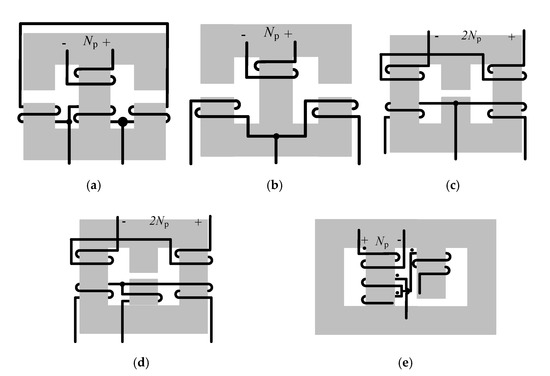
Figure 1.
Structures and winding layout of five integrated magnetic components: (a) structure I, (b) structure II, (c) structure III, (d) structure IV, and (e) structure I–IV.
Figure 1b presents a structure proposed by [12] (hereafter, “Structure II”), in which the primary and secondary windings are wound on different magnetic legs. When conduction occurs on one single side, the primary-side magnetic flux flows to the other leg and generates inductance; accordingly, these transformer windings result in large leakage inductance and thus increase voltage stress on the components. As the output inductance is associated with the turns ratio of the converter, adjustments in the output inductance may involve the number of turns selected for the primary winding in the structure, rendering such adjustments difficult. Moreover, Structure II, in which the self-inductance of the primary winding is the same as that in Structure I, also exhibits large current ripples in the primary winding and hence high losses from primary-side components.
Figure 1c demonstrates a structure developed by [13] (hereafter, “Structure III”), which is an improved version of Structure II. In this structure, the primary winding is separated from the secondary winding; the magnetic flux generated from the primary winding is cancelled out at the center leg and thus can be coupled completely to the secondary winding. This greatly reduces the leakage inductance problem observed in Structure II. In this winding structure, self-inductance on the primary side is related to magnetic reluctance of the outer legs; therefore, this structure alleviates the problem of excessive current ripples in the primary winding. Similarly, to Structure II, the output inductance of Structure III is associated with the converter turns ratio; accordingly, adjustments in the equivalent inductance may require more turns in the primary winding and thus increase loss on the primary side. The total loss for Structure III is in the middle of the total loss values for the three structures.
Figure 1d depicts a structure proposed by [14] (hereafter, “Structure IV”), which has one winding more than Structure III does, providing a more flexible design with equivalent output inductance; this resolves the difficulty in adjusting output inductance for an integrated transformer. Unlike Structure III, Structure IV does not require the number of primary winding turns to be increased for the equivalent output inductance to be increased, and it thus reduces conduction loss. Its total loss is the lowest among the first four structures.
Figure 1e is a structure developed by [15] (hereafter, “Structure V”), in which an EE core transformer and a UI core inductor are integrated into a four-leg core and applied in a phase-shifted full-bridge converter with a center-tap secondary side. This four-leg core is composed of two center legs, one of which is an ungapped second magnetic leg, or left center leg, used for the primary and secondary windings of the transformer; the other is an air-gapped third magnetic leg, or right center leg, used for inductor winding and for the prevention of core saturation. Compared with the aforementioned three-leg-core integrated transformers and inductors, Structure V provides reduced losses from the primary and secondary windings and an intermediate core loss. It thus has the lowest total loss among the five core structures.
For a power output of 1.2 kW, Figure 2 illustrates the total losses of five transformer structures in the same output inductance condition. Among Structures I–IV, Structures I and II exhibit relatively low self-inductance on the primary side and thus larger current ripples on the primary side. In addition, because interleaved winding cannot be used to reduce the amplitude of the magnetomotive force in winding layers for Structure II, it has the highest conduction loss among the first four structures. The winding method in Structure III alleviates the problem observed in Structure II but requires more turns to achieve high output inductance, which contributes to the additional conduction loss in Structure III. Structure IV increases the number of windings to facilitate a flexible output inductance design. Although it yields lower total loss than the first three structures do, it exhibits a high level of conduction loss. Structure V, compared with the other four structures, has relatively high primary-side self-inductance and, thus, smaller current ripple, reducing the AC conduction loss through the interleaved windings; in addition, Structure V facilitates flexible inductor design because of its additional winding and, due to its low magnetic flux density, has a lower hysteresis loss compared with Structure IV. Analysis of and comparison among the five magnetic components reveals that the lowest loss is in Structure V.
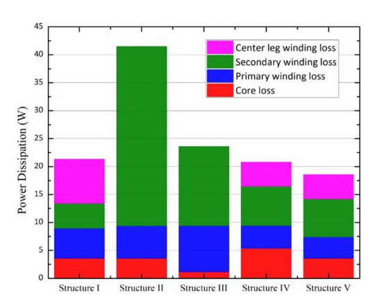
Figure 2.
Comparison of the losses from five integrated magnetic components.
In this study, an integrated transformer in a phase-shifted full-bridge converter with a center-tap secondary side was applied. A transformer and an inductor were integrated into one core to reduce volume, but the mutual inductance between them caused the inductance to vary across switching modes. In Section II of this study, the inductance formula for each time interval is derived, a method is proposed for minimizing the variation of current ripples in core inductors to a level approaching that before the integration, and design steps are consolidated for optimizing loss by selecting an appropriate core volume. Section III reveals the experimental results; describes the application of the integrated core in a phase-shifted full-bridge converter with an input voltage of 400 V, output voltage of 12 V, and output wattage of 1.7 kW; provides an analysis of the loss distribution in the circuit; and verifies the theoretical analyses with the experimental results. Finally, Section IV concludes the study.
2. Operating Theory
Figure 3 illustrates the circuit of a phase-shifted full-bridge converter that has a four-leg-core integrated magnetic component applied in its center-tap secondary side. The section analyzes the equivalent inductance in various intervals during the circuit operation.
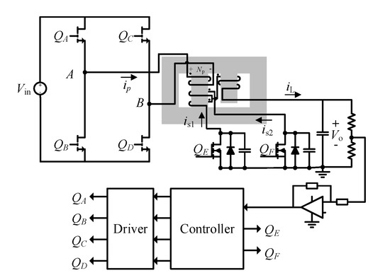
Figure 3.
Application of an integrated magnetic component in a phase-shifted full-bridge converter.
Figure 4a depicts the side view of the magnetic component on which parameters are marked, and Figure 4b presents the equivalent magnetic path model. Each of A1–A5 represents the effective cross-sectional area of a magnetic leg; Rm1–Rm5 represent the reluctance corresponding to each of the respective magnetic legs, and Rm5 is the reluctance between the transformer and inductor, which affects the coupling effect of the two and thus greatly influences the overall magnetic path analysis. To simplify the production and design of a magnetic core, the outer legs are usually designed symmetrically, and the effective cross-sectional area is designed to be half the cross-sectional area of the second leg to satisfy Rm1 = Rm4 = Rm and Rm2 = 0.5Rm. Φ1–Φ5 is the magnetic flux in each leg. The transformer and output inductor windings are wound around the second and third legs, which correspond to A2 and A3, respectively; magnetomotive force is represented by voltage source symbols; Np refers to the number of turns in the converter primary winding P; NS is the number of turns in each of the secondary windings, S1 and S2; and NL is the number of turns in the inductor winding L.
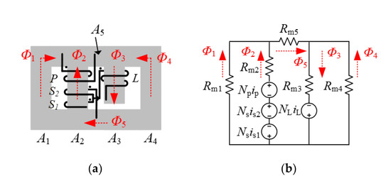
Figure 4.
Integrated magnetic component: (a) Schematic and (b) Equivalent reluctance model.
In a duty cycle of the phase-shifted full-bridge converter shown in Figure 3, the switches must be switched in turn to transfer the energy of the input voltage source Vin to the output voltage source Vo; the converter contains six switching modes, which are marked as modes 1–6 in Figure 5a–f. By marking the corresponding duty interval of each switching mode as intervals 1–6 and the corresponding switching time point as t0–t6, we produced the voltage and current waveforms of the equivalent circuit (Figure 5) in a duty cycle, as shown in Figure 6. For comparison, the corresponding waveform before the transformer and inductor were integrated into one core represented as a dotted line along the iL waveform. Subsequently, the corresponding magnetic flux waveforms for the magnetic paths in Figure 4b in a duty cycle are presented in Figure 6. The various slopes of iL waveforms in time intervals 1–6 reveal that the equivalent inductance differs across intervals, which was attributable to the mutual effects, namely mutual inductance, between the transformer and inductor in the integrated magnetic component. The equivalent inductance of L in intervals 1–6, namely switching modes 1–6, was presented using Leqx, with the x value in the subscript ranging from 1 to 6.


Figure 5.
Six switching modes of the phase-shifted full-bridge converter: (a) Mode 1, (b) Mode 2, (c) Mode 3, (d) Mode 4, (e) Mode 5 and (f) Mode 6.

Figure 6.
Voltage waveform, current waveform, and magnetic flux waveform of each magnetic path during a duty cycle.
The following sections analyze the circuit operation during the six intervals.
Interval 1 (t0 ≤ t < t1)
In this interval, the voltage between the two bridge arms on the primary side (VAB) is the input voltage (Vin). If the equivalent inductance mapped to the primary side from the output inductance is posited to be much higher than the additional resonant inductance, the voltage of the primary winding of the transformer can be assumed to be the input voltage. At this time, the magnetic flux in the second leg is increasing; in addition, because the primary and secondary windings are wound on the same leg, satisfactory coupling between the primary and secondary sides can be assumed. On the basis of this relationship, the voltage of the winding on the third leg (VL) is calculated as in Equation (1). As the voltage of the third-leg winding is greater than 0 in this interval, the magnetic flux in the third leg is also increasing.
Interval 2 (t3 ≤ t < t4)
The voltage between the two bridge arms on the primary side is −Vin. The magnetic flux variation in the third-leg winding during this interval and that in the positive energy transfer interval are both positive. However, the second-leg winding voltage changes from a positive value to a negative one, indicating a slight difference in the equivalent inductance.
Interval 3 (t1 ≤ t < t2)
The voltage between the two bridge arms is short-circuited by the primary-side switches, and the primary winding voltage and the magnetic flux variation in the second leg are therefore both assumed to be zero. Due to the satisfactory coupling between the windings on the second leg, the primary winding voltage is assumed to be zero. According to the loop on the secondary side, the voltage of the third-leg winding is −Vo; in this interval, the magnetic flux variation in the third leg is negative.
Interval 4 (t4 ≤ t < t5)
Interval 4 is mostly identical to interval 3, except that the current of the third-leg winding is changed from the current of winding S1 to that of winding 2. Therefore, the equivalent output inductance in this interval is the same as that in the positive energy transfer interval.
Interval 5 (t2 ≤ t < t3)
The current between the two bridge arms on the primary side changes from a short-circuit state to −Vin. Deduction shows that the transformer winding voltage approaches zero and that the magnetic flux variation in the second leg is zero. Voltage across the additional resonant inductance and the leakage inductance of the transformer, and the third-leg winding voltage is −Vo.
Interval 6 (t5 ≤ t < t6)
Interval 6 is identical to Interval 5 except for the change in the primary winding voltage.
In this study, following operation analysis for each interval, the equivalent inductance and magnetic flux corresponding to each interval were investigated. To prevent saturation, the magnetic flux in each magnetic path must be obtained. As a magnetic flux comprises both DC and AC, they can be calculated separately and the total calculated to determine the magnetic flux in each magnetic path. As DC is present only in the third leg, the DC magnetic fluxes in all windings are provided by the third leg. Accordingly, a reluctance model reveals the DC magnetic flux in each magnetic path; R5, particularly, exerts a major influence on the distribution of DC magnetic fluxes.
An AC magnetic flux, due to its characteristics, can be assumed to provide a current source. The size of such a current source is determined by the volt-second balance of the winding, namely the magnetic flux variation of the winding, and the direction of the current source is determined by the voltage and current directions determined by the winding. Figure 7a–d shows four different AC magnetic flux models. Subsequently, the total of the AC and DC components is calculated to obtain the total magnetic flux of each magnetic path.

Figure 7.
Definition of AC magnetic flux models.
To analyze the equivalent inductance in each interval, the reluctance model in Figure 4b is first used to obtain the magnetic flux formulae for the second and third legs:
Subsequently, per Figure 7, a relationship formula between winding voltage and magnetic flux is established:
According to the definition of inductance, Equation (5) can then be expressed as a relationship formula between inductance and current:
where Lx,y and Mx,y refer to self-inductance and mutual inductance, respectively, and the x and y in the subscript is the code for each winding presented in Figure 4.
Through substitution of the voltage condition for each interval into Equation (6) and use of the definitions for transformer turns ratio (Np/Ns = n) and input voltage ratio (k = nVo/Vin), the winding equivalent inductance in each interval is derived.
The common term in Equations (7)–(12) is substituted with a single variable to obtain Equation (13).
Leq3 (represented as Leqx,Nor) is then normalized and Equations (7)–(12) are reorganized as Equations (14)–(19).
Because k and α are both positive, according to Equations (14)–(19), the smaller α is, the closer the inductance values from after integration and before integration are in each interval. When α = 0, the inductance in each interval is identical before and after integration. This result is also verified with the sensitivity curves of Leq2,Nor in relation to k and α (Figure 8).
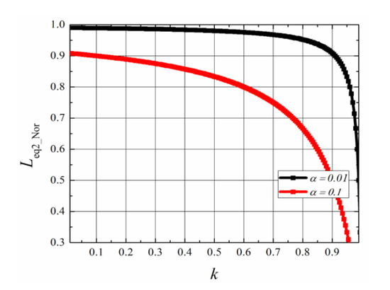
Figure 8.
Sensitivity curves of Leq2,Nor to k and α.
The inductor current waveform in each interval (Figure 6) shows that the inductor current is the largest in Interval 2; therefore, the equivalent inductance in Interval 2 (Leq2) can be adopted as the design inductance (Lo_eff), as illustrated in Equations (20) and (21).
where ΔIL is the inductor ripple current, and fs is the switching frequency of the converter.
For design requirements, Leq2 is simplified. As an air gap is added to the third leg, meaning that Rm3 >> Rm and Rm5, Equation (8) can be simplified to Equations (22) and (23):
Therefore, Equation (23) can be obtained from Equation (17).
3. Design Optimization
According to the theoretical analyses in Section II, in this study, a design optimization procedure (Figure 9) was proposed, in which formulae established by this study were imported to a mathematical software package for calculations. Table 1 lists the output specifications; Vin = 400 VDC, Vo = 12 VDC, output current = 141.6 A, and output power = 1.7 kW, and a PC95 ferrite core were used in the design of an integrated magnetic component.

Figure 9.
Design optimization procedure for an integrated magnetic component.

Table 1.
Phase shift full-bridge converter specification.
On the basis of the design procedure in Figure 9, the integrated ferrite component design was divided into the following five steps.
Step 1:
First, Equation (21) is used for calculation of the inductance before integration that is required for the current ripple requirement to be satisfied. For example, given the specifications fs = 80 kHz, ΔIL = 26 A, Ns = 1, and Np = 24 in this study, we can calculate that n = 24 and Lo_eff = 0.8 μH.
Step 2:
The equivalent inductance in each interval (Figure 6) is calculated using Equations (7)–(12). To maintain the ripple current (iL) within the upper limit, because the equivalent output inductance in a duty cycle is Leq2, we let Leq2 = Lo_eff. In addition, the air gap is assumed to be added to the third leg such that R3 >> R and R5, and α can thus be seen to have an extremely small value; therefore, Leq3 ≅ Leq2 = Lo_eff. Inductance loss caused by the duty cycle must also be prevented from becoming excessively close to α in the design. By the end of Step 2, the equivalent inductance in each interval is obtained.
Step 3:
Reluctance Rm1–Rm5 (Figure 4b) in the respective magnetic paths is calculated. As mentioned in Section II, to simplify the design, we define Rm1 = Rm4 = Rm, Rm2 = 0.5Rm, and
By substituting these definitions into Equations (8) and (9), we obtain the following Equations.
Step 4:
The cross-sectional area of each leg is calculated. As the reluctance of each magnetic path is known by this step, the method for calculating AC and DC, separately described in Section II, is used to determine the magnetic flux in each magnetic path of the ferrite core at full load. As the values of DC and voltage across the windings are known, the calculation of the magnetic flux for each path also involves only NL and β. Furthermore, to initiate the design from the third leg and to prevent ferrite core saturation, we obtain Equations (27) and (28).
where A3_min is the minimum value required for A3, Φ3_max is the maximum working value for Φ3, Bmax is the saturated magnetic flux density specified in the material specifications of the ferrite core, lg is the air gap length in the third leg, and μ0 is the permeability of free space. Substituting different NL and β values into Equations (27) and (28) reveals that A3 and lg are affected mainly by NL and only slightly by β, as depicted in Figure 10a,b. In this study, in which the feasibility of ferrite core volume and air gap length were considered, NL = 2. Accordingly, β was the only variable whose value was undetermined.

Figure 10.
(a) Curve of A3 in relation to NL and β (b) Curve of lg in relation to NL and β.
For the design of the effective cross-sectional area of each leg, two factors should be considered: preventing saturation and hysteresis loss in the ferrite core. Let the subscript y, ranging from 1 to 5, denote the leg; the minimum cross-sectional area required to prevent ferrite core saturation is obtained using Equation (29).
where ΔΦy is the magnetic flux variation in each leg; this variation can be calculated according to the magnetic density variation with a given loss, which is determined using the curve for ferrite core loss volume density (Pcv) against magnetic flux density (By_max; Figure 11). Whichever of Equations (27) and (28) has the greater value is determined as Ay.
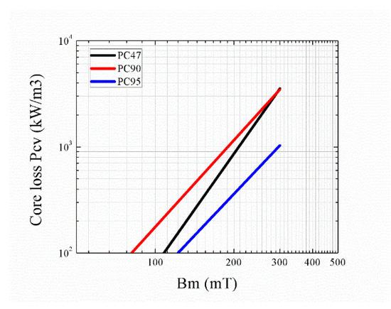
Figure 11.
Curve for Pcv against magnetic flux density.
Step 5:
The volume parameters and ferrite core loss values are substituted into the formulae. Figure 12 presents the top and side views of the ferrite core marked with geometric dimension variables. Let the geometric dimension parameters of the core be as depicted in Figure 12: L, W, and H are the length, width, and height of the ferrite core, respectively, including the windings; a and b are the length and width of the outer legs in the ferrite core, respectively; c is the width of the second and third legs; d is the length of the second and third legs; p is the distance between an outer leg and the nearest center leg; and 2W is the distance between the two center legs. These parameters were used to obtain the area occupied by ferrite core. In this study, H = 30 mm, and according to Figure 12, A1 = A4 = A5 = a × b, and A2 = A3 = c × d. The area of the ferrite core was calculated using Equation (31).
where min(w,p) refers to the smaller value of w and p. To calculate the volume parameters and the total ferrite core loss, an auxiliary variable γ was required. We assumed that γ = w/c, selected a core loss density (Pcv), and substituted β and γ into the calculation to obtain the total size and loss of the ferrite core. Figure 13a presents the results obtained for Pcv = 400 kW/m3 and with the substitution of various β and γ values into the calculation. When the area is constant, each β value corresponds to one γ value, and β is therefore represented on the x-axis. With different total areas, the minimum loss corresponds to different β values. Hence, the β values corresponding to the minimum loss for various Pcv values were plotted in Figure 13b. In this manner, the appropriate total area and the Pcv, β, and γ values for the area were determined. With the total size and loss of the circuit considered, the magnetic component parameters were determined as follows for the experiment in this study: area = 1300 mm2 and Pcv = 400 kW/m3.

Figure 12.
Geometric dimensions of the ferrite core: (a) top view and (b) side view.

Figure 13.
Core loss graph with β and γ substituted into the calculation: (a) curve representing loss according to β value for various core areas; (b) curve representing loss according to area for various Pcv values.
4. Experimental Verification
This section details the application of Structure V, an integrated four-leg magnetic component, in a center-tap phase-shifted full-bridge converter with an input voltage of 400 VDC, output voltage of 12 VDC, and output power of 1.7 kW; an analysis on the loss of the converter; and a test on parameters, including efficiency. Table 2 illustrates the geometric dimensions of the ferrite core designed in accordance with the aforementioned five steps.
Table 2.
Design Parameters of Proposed Transformer Structure.
Figure 14a presents the phase-shifted full-bridge converter in which the ferrite core was used for the experiment, Figure 14b shows the integrated ferrite core for the converter, and Table 3 lists the specifications used in the converter design.

Figure 14.
Phase-shifted full-bridge converter with an integrated transformer: (a) Physical circuit; (b) Ferrite core.
Table 3.
Design parameters of phase shift full-bridge converter.
Figure 15 depicts the experimental efficiency of the novel phase-shifted full-bridge converter with an integrated transformer; the curve peaks at 96.7% in the half-load condition. Although wide band gap components greatly reduced the hard switching loss in the light-load condition, switching loss and ferrite core hysteresis loss remained the main sources of loss in the light-load condition. The integrated ferrite core reduced the distance between the center tap and the inductor contact, which reduced loss along the path in the half-to-full-load condition.
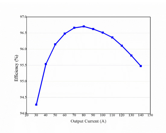
Figure 15.
Efficiency curve for the phase-shifted full-bridge converter with an integrated transformer.
Figure 16 depicts the loss distribution in 20%, 50%, and 100% load conditions. A model was used to calculate losses, including the hysteresis loss of the transformer and conduction loss in the copper wire, according to the experimental measurements. According to the calculation results, the secondary winding loss of the transformer accounted for most of the total loss.

Figure 16.
Loss distribution.
Figure 17a depicts the switching waveforms of the leading bridge arm switch in various load conditions. When the output load was greater than 45 A, the leading bridge arm switch achieved ZVS, and no Miller plateau was observed in the switch gate voltage. Figure 17b reveals the switching waveforms of the lagging bridge arm switch in various load conditions. As seen in Figure 17a, hard switching was implemented; to improve efficiency, the dead time was designed to occur between the switch series resonance and the wave trough to reduce the loss incurred from hard switching. When the load current was greater than 80 A, the lagging bridge arm switch achieved ZVS, and no Miller plateau was observed in the switch gate voltage. Figure 17c presents the waveforms of the novel converter with an integrated transformer in the full-load condition. A measurement of the current ripples in the output inductor revealed waveforms similar to the analysis result proposed in Section II. The actual equivalent inductance was determined from the slope of the current.
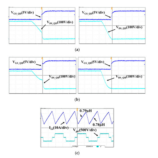
Figure 17.
Measured waveforms: (a) Turn on transient of low side switch of leading leg at 30 and 45 A output load. (b) Turn on transient of low side switch of lagging leg at 45 and 80 A output load (c) output capacitor current ripple at full output load.
In the full-load condition, the temperatures of the main components were as shown in Figure 18. The temperature of the bridge arm switch was approximately 43 °C (Figure 18a); the highest temperature was observed in the secondary winding of the transformer at 94 °C (Figure 18b).

Figure 18.
Measured temperatures: (a) primary-side switch and (b) secondary winding of the transformer.
5. Conclusions
This study involved the application of a four-leg ferrite core that integrated a transformer and an inductor on a center-tap phase-shifted full-bridge converter and the analysis of the integrated transformer and formulae in six switching modes. Subsequently, a method was proposed for determining the dimensions of the ferrite core and, according to the resultant core volume, a design procedure was established for optimizing component loss. A converter was used to verify the performance of the proposed integrated transformer; analyze the loss distribution of the transformer; and measure relevant parameters including the waveform and efficiency to validate the proposed design procedure. Finally, in accordance with the design optimization procedure, an integrated magnetic component was designed and applied in a phase-shifted full-bridge converter to achieve an input voltage of 400 VDC, output voltage of 12 VDC, output power of 1.7 kW, and switching frequency of 80 kHz. The highest conversion efficiency achieved by the converter was 96.7%, and the power density was 150 W/inch3.
Author Contributions
Y.-C.L. and C.-Y.X. conceived and designed the prototype and experiments; C.-Y.X., C.-C.H., P.-C.C. performed the experiments; Y.-C.L.; C.-Y.X. analyzed the data; Y.-C.L., C.-Y.X., C.-C.H., and H.-J.C. contributed equipment/materials/analysis tools; Y.-C.L.; C.-Y.X. and C.-C.H. wrote the paper. All authors have read and agreed to the published version of the manuscript.
Funding
This work was supported in part by the Ministry of Science and Technology, Taiwan under Grant 109-2221-E-197 -014 - and 109-2221-E-002 -097 -.
Institutional Review Board Statement
Not applicable.
Informed Consent Statement
Not applicable.
Data Availability Statement
Not applicable.
Conflicts of Interest
The authors declare no conflict of interest. The funders had no role in the design of the study; in the collection, analyses, or interpretation of the data; in the writing of the manuscript, or in the decision to publish the results.
References
- Yang, B.; Lee, F.C.; Zhang, A.J.; Huang, G. LLC resonant converter for front end DC/DC conversion. In Proceedings of the APEC Seventeenth Annual IEEE Applied Power Electronics Conference and Exposition (Cat. No. 02CH37335), Dallas, TX, USA, 10–14 March 2002; IEEE: Piscataway, NJ, USA, 2002; pp. 1108–1112. [Google Scholar]
- Yang, B.; Chen, R.; Lee, F.C. Integrated magnetic for LLC resonant converter. In Proceedings of the APEC Seventeenth Annual IEEE Applied Power Electronics Conference and Exposition (Cat. No. 02CH37335), Dallas, TX, USA, 10–14 March 2002; IEEE: Piscataway, NJ, USA, 2002; pp. 346–351. [Google Scholar]
- Lu, B.; Liu, W.; Liang, Y.; Lee, F.C.; Van Wyk, J.D. Optimal design methodology for LLC resonant converter. In Proceedings of the Twenty-First Annual IEEE Applied Power Electronics Conference and Exposition, 2006. APEC ’06, Dallas, TX, USA, 19–23 March 2006; IEEE: Piscataway, NJ, USA, 2006; pp. 533–538. [Google Scholar]
- Redl, R.; Sokal, N.O.; Balogh, L. A novel soft-switching full-bridge DC/DC converter analysis, design consideration, and experimental results at 1.5 kW, 100 kHz. IEEE Trans. Power Electron. 1991, 6, 408–418. [Google Scholar] [CrossRef]
- Redl, R.; Balogh, L.; Edwards, D.W. Switch transitions in the soft-switching full-bridge PWM phase-shift DC/DC converter: Analysis and improvements. In Proceedings of the Intelec 93: 15th International Telecommunications Energy Conference, Paris, France, 27–30 September 1993; IEEE: Piscataway, NJ, USA, 2002; pp. 350–357. [Google Scholar]
- Redl, R.; Balogh, L.; Edwards, D.W. Optimum ZVS full-bridge dc/dc converter with PWM phase-shift control: Analysis, design considerations, and experimentation. In Proceedings of the 1994 IEEE Applied Power Electronics Conference and Exposition—ASPEC’94, Orlando, FL, USA, 13–17 February 1994; IEEE: Piscataway, NJ, USA, 2002; pp. 159–165. [Google Scholar]
- Cho, J.G.; Sabate, J.A.; Lee, F.C. Novel full bridge zero-voltage transition PWM DC/DC converter for high power applications. In Proceedings of the 1994 IEEE Applied Power Electronics Conference and Exposition-ASPEC’94, Orlando, FL, USA, 13–17 February 1994; IEEE: Piscataway, NJ, USA, 2002; pp. 143–149. [Google Scholar]
- Ruan, X.; Liu, F. An improved ZVS PWM full-bridge converter with clamping diodes. In Proceedings of the 2004 IEEE 35th Annual Power Electronics Specialists Conference (IEEE Cat. No.04CH37551), Aachen, Germany, 20–25 June 2004; IEEE: Piscataway, NJ, USA, 2004; pp. 1476–1481. [Google Scholar]
- Badstuebner, U.; Biela, J.; Faessler, B.; Hoesli, D.; Kolar, J.W. An optimized 5kW, 147 W/in3 telecom phase-shift DC-DC converter with magnetically integrated current doubler. In Proceedings of the 2009 Twenty-Fourth Annual IEEE Applied Power Electronics Conference and Exposition, Washington DC, USA, 15–19 February 2009; IEEE: Piscataway, NJ, USA, 2009. [Google Scholar]
- Badstuebner, U.; Biela, J.; Faessler, B.; Hoesli, D.; Kolar, J.W. Optimization of a 5 kW telecom phase shift DC–DC converter with magnetically integrated current doubler. IEEE Trans. Ind. Electron. 2001, 58, 4736–4745. [Google Scholar] [CrossRef]
- Sun, J.; Webb, K.F.; Mehrotra, V. Integrated magnetics for current-doubler rectifiers. IEEE Trans. Power Electron. 2004, 19, 582–590. [Google Scholar] [CrossRef]
- Chen, W.; Hua, G.; Sable, D.; Lee, F.C. Design of High Efficiency, Low Profile Low Voltage Converter with Integrated Magnetics. In Proceedings of the APEC 97-Applied Power Electronics Conference, Atlanta, GA, USA, 27 February 1997; IEEE: Piscataway, NJ, USA, 2002. [Google Scholar]
- Xu, P.; Wu, Q.; Wong, P.L.; Lee, F.C. A novel integrated current doubler rectifier. In Proceedings of the APEC 2000. Fifteenth Annual IEEE Applied Power Electronics Conference and Exposition (Cat. No.00CH37058), New Orleans, LA, USA, 6–10 February 2000; IEEE: Piscataway, NJ, USA, 2000; Volume 2, pp. 735–740. [Google Scholar]
- Sun, J.; Webb, K.F.; Mehrotra, V. An improved current-doubler rectifier with integrated magnetics. In Proceedings of the APEC. Seventeenth Annual IEEE Applied Power Electronics Conference and Exposition (Cat. No. 02CH37335), Dallas, TX, USA, 10–14 March 2002; IEEE: Piscataway, NJ, USA, 2002; pp. 831–837. [Google Scholar]
- Lu, Z.; Yang, H.; Zhang, A.J. New magnetic integration of full-wave rectifier with center-tapped transformer. In Proceedings of the 2014 International Power Electronics and Application Conference and Exposition, Shanghai, China, 5–8 November 2014; IEEE: Piscataway, NJ, USA, 2015. [Google Scholar]
- Pietkiewicz, A.; Tollik, D. Coupled-inductor current-doubler topology in phase-shifted full-bridge dc–dc converter. In Proceedings of the INTELEC-Twentieth International Telecommunications Energy Conference (Cat. No. 98CH36263), San Francisco, CA, USA, 4–8 October 1998; IEEE: Piscataway, NJ, USA, 2002; pp. 41–48. [Google Scholar]
- Wong, P.L.; Wu, Q.; Xu, P.; Yang, B.; Lee, F.C. Investigating coupling inductors in the interleaving QSW VRM. In Proceedings of the APEC 2000. Fifteenth Annual IEEE Applied Power Electronics Conference and Exposition (Cat. No.00CH37058), New Orleans, LA, USA, 6–10 February 2000; IEEE: Piscataway, NJ, USA; pp. 973–978. [Google Scholar]
- Wong, P.L.; Lee, F.C.; Jia, X.; Van Wyk, D. A novel modeling concept for multi-coupling core structures. In Proceedings of the APEC 2001. Sixteenth Annual IEEE Applied Power Electronics Conference and Exposition (Cat. No.01CH37181), Anaheim, CA, USA, 4–8 March 2001; IEEE: Piscataway, NJ, USA, 2002. [Google Scholar]
- Xu, P.; Lee, F.C. Design of high-input voltage regulator modules with a novel integrated magnetic. In Proceedings of the APEC 2001. Sixteenth Annual IEEE Applied Power Electronics Conference and Exposition (Cat. No.01CH37181), Anaheim, CA, USA, 4–8 March 2001; IEEE: Piscataway, NJ, USA, 2002; Volume 1. [Google Scholar]
- Xu, P.; Ye, M.; Lee, F.C. Single Magnetic Push-Pull Forward Cooveener Fatunng Built-in Input Filter and Coupled-Inductor Current Doubler for 48V VRM. In Proceedings of the IEEE Applied Power Electrooics Conference and Exposition (APEC’02), Dallas, TX, USA, 10–14 March 2002; IEEE: Piscataway, NJ, USA, 2002. [Google Scholar]
- Xu, P.; Ye, M.; Wong, P.L.; Lee, F.C. Design of 48 V voltage regulator modules with a novel integrated magnetics. IEEE Trans. Power Electron. 2002, 17, 990–998. [Google Scholar]
- Zhou, H.; Wu, T.X.; Batarseh, I.; Ngo, K.D. Comparative investigation on different topologies of integrated magnetic structures for current-doubler rectifier. In Proceedings of the 2007 IEEE Power Electronics Specialists Conference, Orlando, FL, USA, 17–21 June 2007; IEEE: Piscataway, NJ, USA, 2007; pp. 337–342. [Google Scholar]
Publisher’s Note: MDPI stays neutral with regard to jurisdictional claims in published maps and institutional affiliations. |
© 2020 by the authors. Licensee MDPI, Basel, Switzerland. This article is an open access article distributed under the terms and conditions of the Creative Commons Attribution (CC BY) license (http://creativecommons.org/licenses/by/4.0/).