1. Introduction
DC-DC converters [
1,
2,
3] are commonly used to supply power electronics devices. One of the most popular types of these converters is a boost converter. This converter allows obtaining the output voltage higher than the input voltage while maintaining high conversion efficiency [
1,
2,
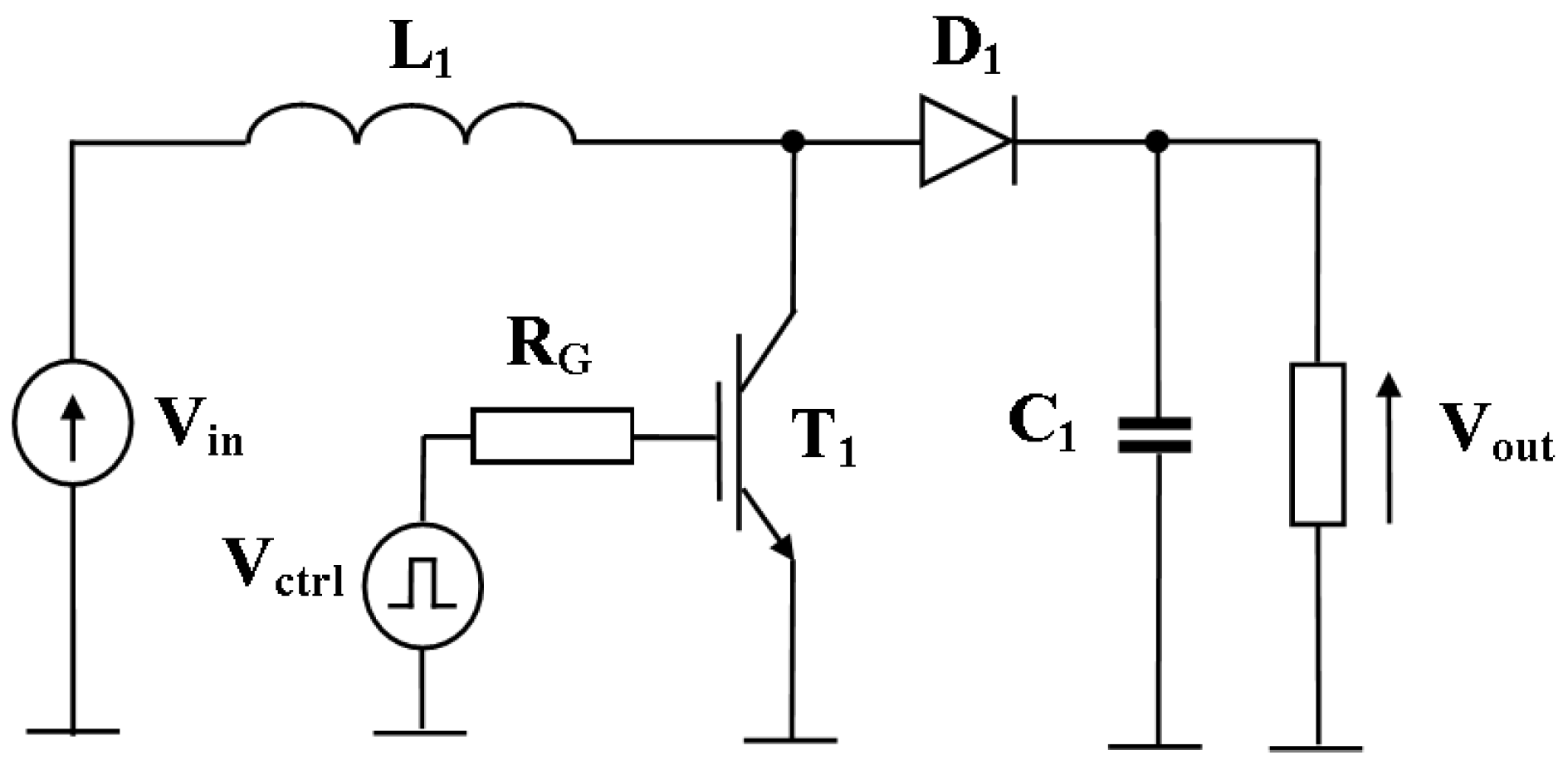
3]. The diagram of the considered converter is shown in
Figure 1.
At the designing stage of all electronic systems, including DC-DC converters, computer simulations are necessary [
1,
4,
5]. One of the most popular simulation programs used in electronics is SPICE (Simulation Program with Integrated Circuit Emphasis) [
4,
6]. One of its greatest advantages, compared to other popular simulation environments [
7], is the ability to easily implement any compact model of an electronic component. Unfortunately, the models included in the SPICE program are isothermal, i.e., they do not take into account thermal phenomena. In these models, the junction temperature of the component is constant and does not depend on the power dissipated in it. In order to take into account thermal phenomena in computations, the SPICE program formulates models called electrothermal in the form of subcircuits for this program. The second significant disadvantage of the models built into the SPICE program is their limited accuracy, resulting from the simplified modelling of some important physical phenomena occurring in the component, which for the Insulated Gate Bipolar Transistor (IGBT) was presented, among others, in the paper [
8].
The methods of estimating the internal temperatures of semiconductor devices using the model-order reduction techniques are described in the paper [
9]. In turn, the methods of behavioural electrothermal modelling of power devices are described in the paper [
10], whereas the methods of electrothermal simulations of switch-mode power converters are considered in the paper [
11].
Performing the transient analysis of DC-DC converters in SPICE using the built-in models of electronic components is time-consuming. As it results from the paper [
9], the time required to perform the computations to an electrically steady state is equal to even 24 h. From the engineering point of view, this is an unacceptably long time. Therefore, for many years, scientists have been conducting research on new methods of analysis that will allow reducing this time to an acceptable value [
10,
11,
12,
13,
14,
15,
16]. These methods consist of modifying the classic method of transient analyses of electronic networks [
10,
11,
13]. They use special algorithms to predict values of voltages and currents at the steady state.
Yet, another way is to use the method of a DC analysis with the averaged models of semiconductor devices or the whole electronic systems [
12,
13,
14,
16,
17]. Using this method, it is possible to achieve a significant reduction in the computation time while maintaining the accuracy of computations of static characteristics.
One of such methods is a method using the averaged model of the diode–transistor switch [
12,
16,
17], which is included in each single-inductor DC-DC converter, e.g., a boost converter, the diagram of which is shown in
Figure 1. In such a model, the observation is used that at operation of the converter, the diode and the transistor contained in it conduct the current alternately, and for each of these devices associated with subcircuits, the equations describing the average values of voltages and currents of the converter in the steady state are formulated [
3,
17]. The following assumptions are made when formulating the equations constituting the average models used in the analysis of DC-DC converters:
- (a)
The formulated equations apply to the converter operation in the steady state,
- (b)
The equations take into account only DC components (average values) of voltages and currents,
- (c)
The switching times of semiconductor devices are negligibly short.
The equations of the model are obtained by equating to zero the dependences describing the average values of voltage on inductors and the average values of the capacitor currents occurring in the modelled network.
Averaged models of the diode–transistor switch have been described in the literature for many years, and the results of computations performed using such models are described for different DC-DC converters [
3,
12,
17,
18,
19,
20,
21,
22,
23,
24,
25,
26]. However, until recently, such models were formulated only for converters containing ideal switches [
3,
17,
18,
19,
20,
21,
22] or Metal Oxide Semiconductor Field Effect Transistors (MOSFETs) [
12,
23,
24,
25,
26], although IGBTs are not less popular in this application [
27,
28,
29,
30]. It is worth noting that when using models of ideal switches, it is impossible to compute the junction temperature of the diode and the transistor operating in the DC-DC converter. Meanwhile, the information about the values of these temperatures is important for the designer of the system and it allows verifying the correctness of the design. A diode–transistor switch with an IGBT requires a different approach than for MOSFET, e.g., for modelling the output characteristics, which results from their different shapes.
The main advantage of the averaged electrothermal model of a diode–transistor switch is short time of computations, which typically does not exceed 0.1 s. Nonetheless, this kind of model has some drawbacks. These drawbacks include neglecting dynamic effects in the thermal behaviour, impossibility of monitoring voltage on the transistor gate to observe a possible dielectric breakdown, and omitting the parasitic capacitances of semiconductor devices. Therefore, the averaged models may be useful to designers who need a fast and accurate estimation of the converter characteristics and verification that the semiconductor devices operate within their safe operating area.
The papers [
31,
32] propose a model of a diode–transistor switch for the analysis of DC-DC converters containing an IGBT. The model presented in [
31] is a simplified model. In this model, a simplified method of describing the output characteristics of the transistor was used, and the influence of thermal phenomena is not taken into account. The main disadvantages of the model from [
31] were removed in its next version, which are presented in [
32]. However, this model does not take into account some important physical phenomena that may significantly affect the accuracy of computations using this model. The correctness of the cited model was verified only in a limited range of load current changes and at one value of the control signal frequency equal to 10 kHz.
This article analyses the influence of the accuracy of selected factors on the accuracy of the computations of the boost converter characteristics made with the use of the model from [
32] under various operating conditions.
Section 2 presents the model under consideration,
Section 3 describes the measurement system used to verify the correctness of this model. Furthermore, in
Section 4, the computed and measured characteristics of the boost converter in a wide range of changes in the load current and frequency of the control signal are presented. We also comment on the reasons for the discrepancies between the results of computations and measurements. A method of reducing these discrepancies is proposed, and their effectiveness is demonstrated in practice.
2. Considered Model
As it was mentioned above, in order to compute the DC characteristics of DC-DC converters, the averaged electrothermal models of a diode–transistor switch can be effectively used. The considered electrothermal model of the diode–transistor switch proposed in [
32] is based on the known concept, which was previously presented for the MOSFET and the ideal lossless switch described, among others, in the papers [
16,
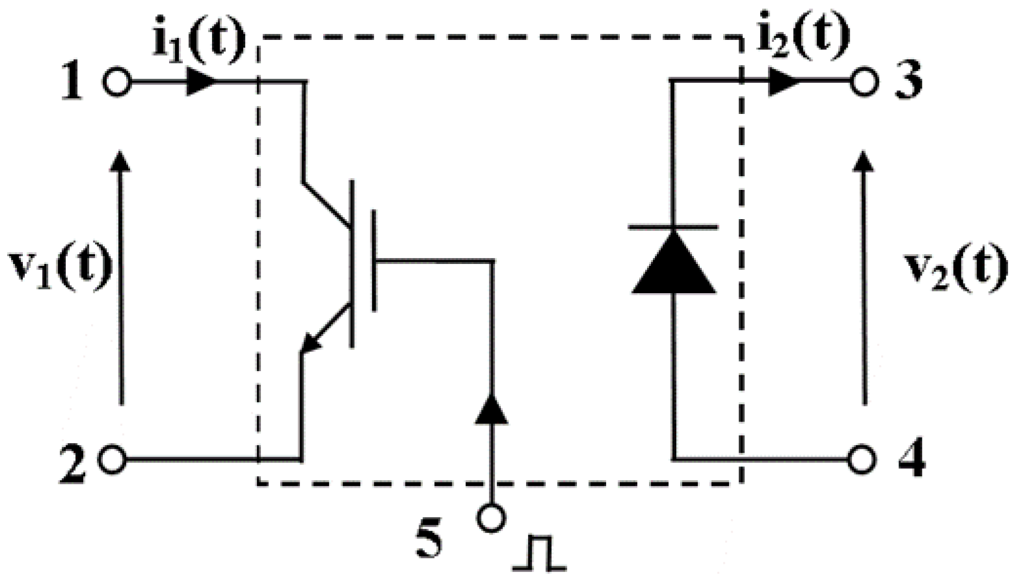
24]. This model allows determining the DC characteristics of any DC-DC converter containing a diode–transistor switch and junction temperature of the semiconductor devices contained therein. The diagram of this switch is shown in
Figure 2.
The network representation of the considered electrothermal averaged model of a diode–transistor switch (AVG model) is shown in
Figure 3. This switch contains an IGBT and a diode.
Terminals 1, 2, 3, and 4 of the AVG model correspond to the terminals of the IGBT and the diode visible in the diagram of the diode–transistor switch shown in
Figure 2. The considered model is connected to other components of the analysed DC-DC converters, using these terminals according to the respective diagrams. The frequency f and the duty cycle d of the signal controlling a DC-DC converter are parameters of the AVG model. These parameters that are used occur in the formulas describing some controlled voltage and current sources in this model. Internal temperatures of the IGBT and the diode correspond to voltages on terminals T
jT and T
jD, respectively.
The described model contains four blocks: main circuit, aided block, thermal model, and CCM/DCM.
The main circuit contains two controlled voltage sources E
R and E
T and the controlled current source G
D. These voltage sources model the average voltage between the collector and the emitter of the IGBT, whereas the current source models the average value of the diode current. V1 is the voltage source of zero value that monitors this current. I
1av and I
2av, as well as V
1av and V
2av in the main circuit, denote the average values of voltages and currents of the semiconductor devices. The output values of the controlled voltage and current sources are described with the equations formulated using the idea presented in the papers [
12,
24]. According to this idea, at the steady state in each period T of the control signal, the current flows through one semiconductor device only. The transistor current flows for the time equal to d·T, and the diode current—for the time (1 − d)·T (in CCM (Continuous Conduction Mode) or less in DCM (Discontinuous Conduction Mode)). In the considered model, the current–voltage characteristics of both the semiconductor devices are described by piecewise linear functions. These functions use parameters depending on the internal temperatures of these semiconductor devices. Values of these parameters are computed in the aided block. In turn, internal temperatures of the diode and the IGBT are computed in the thermal model. The value of the equivalent duty cycle V
eu is computed in the controlled voltage source E
u included in the CCM/DCM block. The output value of this source depends on the parameters control signal—the duty cycle d and frequency f of the control signal, as well as inductance L of the inductor contained in the analysed DC-DC converter and load resistance of this converter.
The internal temperature of the IGBT (T
jT) and the diode (T
jD) are computed in the thermal model with self-heating phenomena taken into account. This model uses the electrical analogue of a DC compact thermal model [
1,
33]. In this analogue, voltages T
jT and T
jD correspond to internal temperatures of the IGBT and the diode, respectively. In turn, the average values of power dissipated in these semiconductor devices are represented by the controlled current sources G
TT and G
TD. The output currents of these sources are described as follows [
32].
where V
IGBT, V
D, R
D, and R
IGBT describe the parameters of piecewise linear models of the transistor and the diode characteristics.
The efficiency of the removal of heat generated in these devices is characterised by thermal resistance represented by resistors RthT and RthD. The voltage source VTa represents ambient temperature.
The other equations describing the controlled sources presented in
Figure 3 are in [
32].
3. Measurement Setup
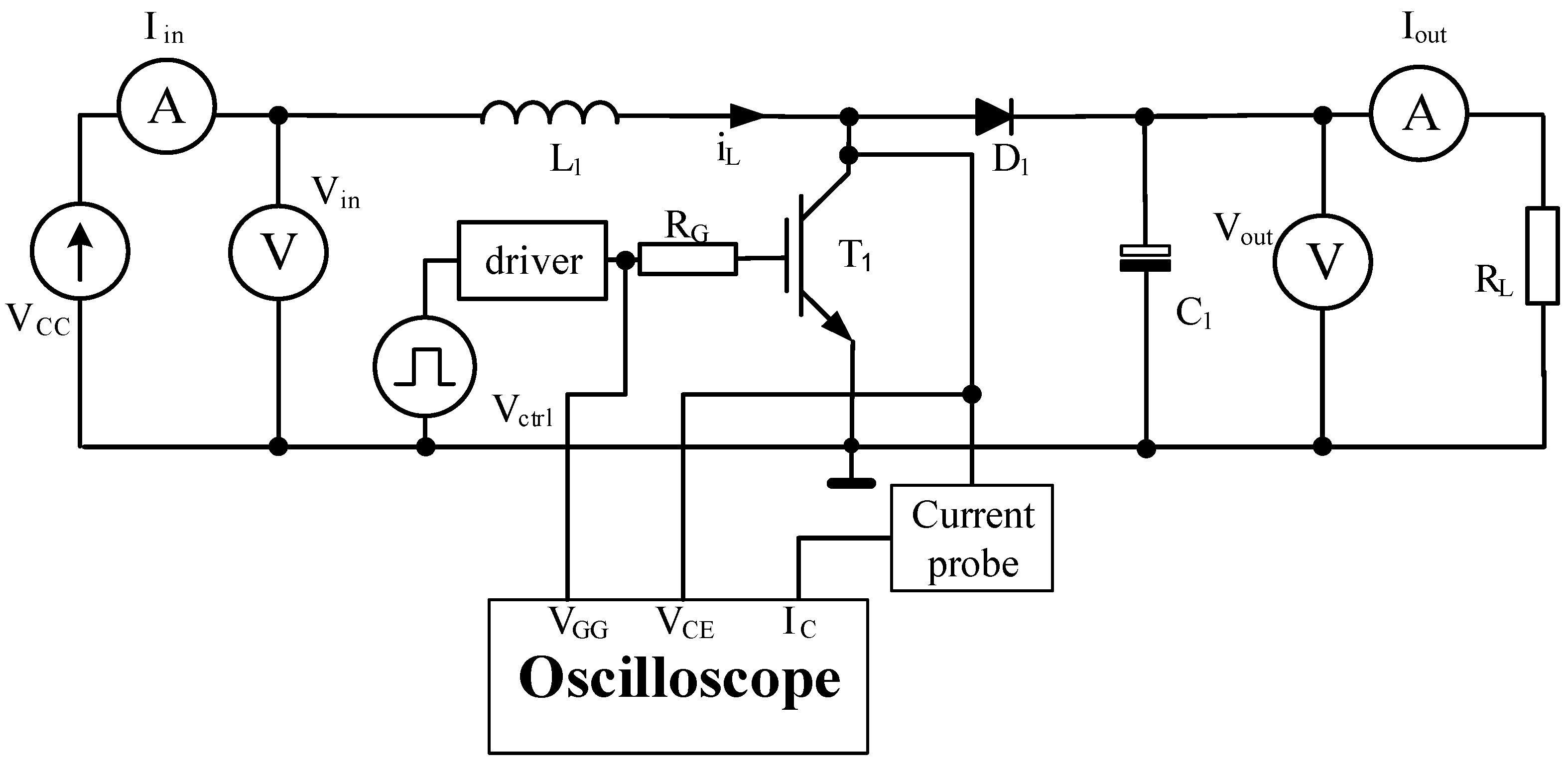
In order to evaluate the usefulness of the considered model, the characteristics of the boost converter containing the considered semiconductor devices are measured and computed. The diagram of the investigated converter is presented in
Figure 4.
In the considered converter, the input voltage VCC is supplied from the GWInstek PSB-2800L power supply. Appa 208 multimeters are used as ammeters and voltmeters. The inductance of coil L1 is equal to 560 μH, and the capacitance of C1 is 1 mF. The voltage controlling the IGBT Vctrl is produced by the NDN C5603P function generator and connected to the gate of the IGBT via the driver IR2125. The prototype is mounted on the Printed Circuit Board (PCB). The diode of the type IDP08E65 is characterised by the maximum repetitive peak reverse voltage equal to 650 V and the maximum forward current equal to 16 A, and the IGBT of the type IGP06N60T is characterised by the maximum collector–emitter voltage equal to 600 V and the maximum DC collector current equal to 12 A. Based on the data given in the datasheet, the maximum switching frequency of this IGBT is estimated as equal to 500 kHz. Some waveforms of voltages and currents of the investigated DC-DC converter were measured using an oscilloscope Rigol MS05104 and a current probe Tektronix PCPA 300 for different values of load resistance and parameters of the control signal.
In order to determine the internal temperature T
j of the IGBT (T
jT) or the diode (T
jD), the case temperature T
C of these semiconductor devices is measured using a pyrometer PT-3S by Optex. Next, using the values of thermal resistances junction-ambient R
thj−a and junction-case R
thj−c, the values of temperature T
j are calculated using the following formula [
7]
where T
a denotes ambient temperature. Values of thermal resistance R
thj−c are given in the data provided by the manufacturer, whereas thermal resistance R
thj−a is measured with the use of indirect electrical methods described e.g., in the paper [
34].
The investigated DC-DC converter operates without any feedback loop, which is typically used in switch-mode power supplies including such converters. Therefore, at the selected operating conditions, the influence of changes in the load resistance and parameters of the control signal are not compensated for by the feedback loop. For this reason, any disadvantages of the considered model can be clearly illustrated for the investigated circuit.
4. Investigation Results
In order to analyse the usefulness range of the model from [
32], hereinafter referred to as the AVG model, computations and measurements of the characteristics of the boost converter in various operating conditions are performed. In particular, the change of the following operating parameters of the considered converter is taken into account: input voltage V
in, load resistance R
L, frequency f, and the duty cycle d of the IGBT control signal. The measurements are carried out for a transistor and a diode operating at different cooling conditions. The operation of the investigated converter in both the CCM (Continuous Conduction Mode) and the DCM (Discontinuous Conduction Mode) [
2] is considered.
The computations were performed for parameters with values identical to those given in [
32], with the stipulation that the values of the model parameters R
thD and R
thT correspond to thermal resistances of the transistor and the diode. For the considered elements placed on heat sinks of the dimensions of 7.5 cm × 5 cm × 3.5 cm, the values of these parameters were 6.2 K/W, and for the devices operating without a heat sink, it was 43.85 K/W.
Selected results of measurements and computations of the investigated DC-DC converter are illustrated in the successive figures. In all these figures, points denote the results of measurements, whereas solid lines denote the results of computations performed with the AVG model.
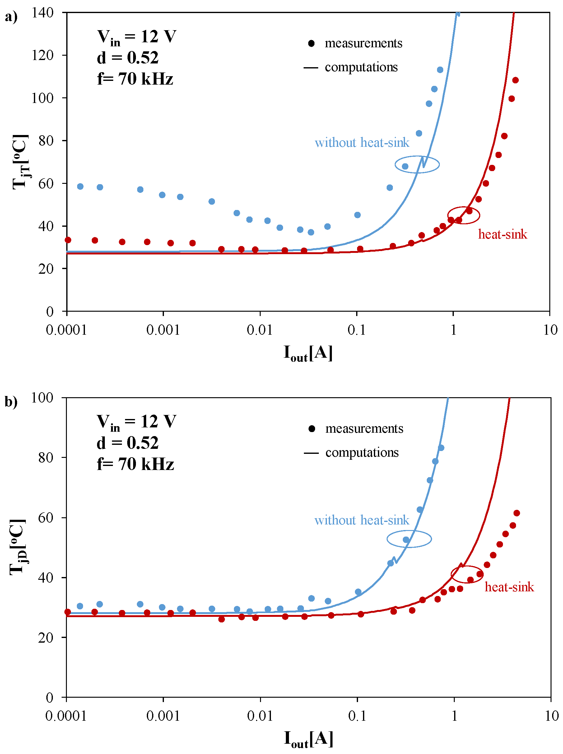
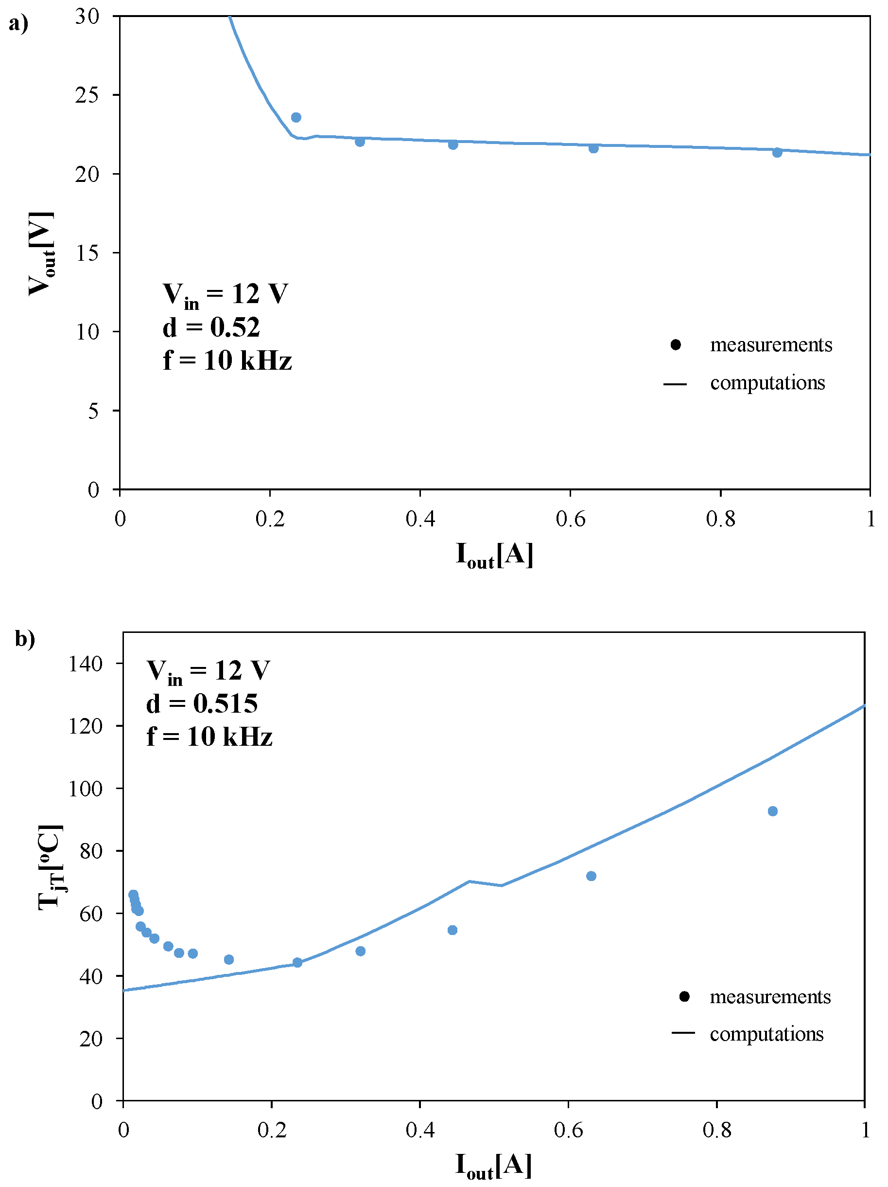
Figure 5 shows the output characteristics of a boost converter operating with low input voltage V
in = 12 V under various cooling conditions, and
Figure 6 shows the corresponding dependences of junction temperature of the transistor (a) and the diode (b) on the output current.
As it results from the data presented in
Figure 5 and
Figure 6, the AVG model correctly reproduces the output characteristics of a boost converter operating in the CCM and the DCM, but only for the output current higher than 10 mA. For lower values of this current, there are significant discrepancies between the results of computations and measurements. The source of these discrepancies is losses resulting from switching off the IGBT omitted when formulating the considered model. The effect of these losses is an increase in the temperature of the transistor despite a decrease in the current value of the IGBT, as shown in
Figure 6a. In order to improve the accuracy of modelling this characteristic, the heat generation model should take into account not only power losses related to the conduction of the IGBT but also power losses resulting from its switching. The method of modelling losses associated with the transistor switching for the needs of the averaged diode-transistor switch model is presented in [
27] for the MOSFET transistor. In the range of very low values of the I
out current, the cause of the discrepancy may also be the omission of leakage currents of the transistor and the diode at the stage of formulating the considered model.
As shown in
Figure 5, the cooling conditions do not significantly affect the shape of the V
out(I
out) dependence for I
out > 1 mA. However, they significantly affect the efficiency of heat removal from the semiconductor devices contained in the considered converter. As shown in the range of very low values of I
out current, an increase in temperature T
jT is visible, which proves that an average value of the dissipated power is as much as 0.5 W.
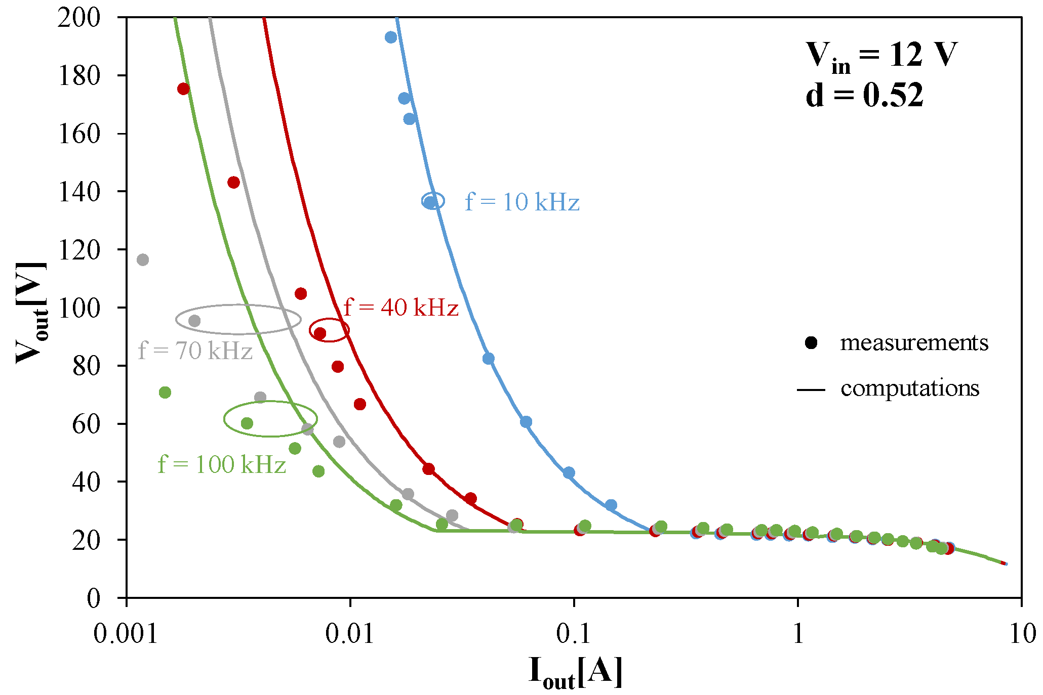
Figure 7 shows the output characteristics of the considered converter for four values of the IGBT switching frequency. Computations and measurements are performed for the transistor and the diode placed on heat sinks.
The results of computations and measurements presented in
Figure 7 prove that for the collector currents below 10 mA and for switching frequencies higher than 10 kHz, the measurement results differ significantly from the results of computations made with the use of the AVG model. For the constant value of the output current, the discrepancy between the computations and measurements results increases with the switching frequency of the IGBT. An increase in the discrepancy also results from the fact that with an increase of switching frequency, the value of the current switched off by the transistor decreases [
2]. A measure of this discrepancy is the relative error in determining voltage δV
out calculated from the formula
where V
outmeasured denotes the measured value of the output voltage, whereas V
outcomputed is the value of this voltage computed with the use of the AVG model.
The computation error of the output voltage as a function of the output current is shown in
Figure 8.
As it can be seen from the data presented in
Figure 8, the relative error of determining the output voltage using the AVG model decreases with an increase of the output current of the boost converter and a decrease of frequency in the CCM. The error δV
out does not exceed a few percent. The graph has clear minima and maxima resulting from the modelling of the output characteristics of the turned-on IGBT using the piece-wise linear function. The smallest error values occur for a switching frequency equal to 10 kHz, and the highest error values occur for the highest among the considered frequencies, which is related to the AVG model not taking into account the influence of parasitic capacitances in the IGBT on the characteristics of the considered DC-DC converter.
Figure 9 shows the dependence of the output voltage of the boost converter on the duty cycle of the signal controlling the transistor contained in it. During the measurements, the considered converter operated with the input voltage of 48 V. The IGBT and the diode were placed on the heat sinks, and the measurements were made for two values of load resistance. Additionally, in
Figure 10a, the dashed line marks the results of computations made in the SPICE program using the AVG model, to which are added the values of the junction temperature increase ∆T
j resulting from dynamic losses in the IGBT computed on the basis of the Equations (5) and (6).
where T
jcond is the value of the IGBT junction temperature computed using the AVG model, R
thj−a is the IGBT thermal resistance junction—ambient, and P
swt is the mean value of the power dissipated in the IGBT resulting from switching losses.
The values of E
on and E
off necessary for the computations were obtained by approximating with linear functions the dependencies presented in the datasheet of the considered IGBT [
35]. Due to the sawtooth shape of the collector current of the IGBT operating in the boost converter, it was necessary to separately determine the value of the switched currents I
on and I
off. The following formulas were used for this purpose [
2].
The results presented in
Figure 10a prove that even with the correctly determined values of the converter output voltage, which are shown in
Figure 9, the computations of the corresponding values of the IGBT junction temperature may be characterised by a big error. The reason for this error is the omission of switching losses in the heat generation AVG model. In the case of the IGBT operation with high switching frequency, switching power losses that are proportional to e.g., to frequency and the switched current, can be much higher than the conduction losses of the IGBT [
36,
37]. This is demonstrated by the computation results presented in
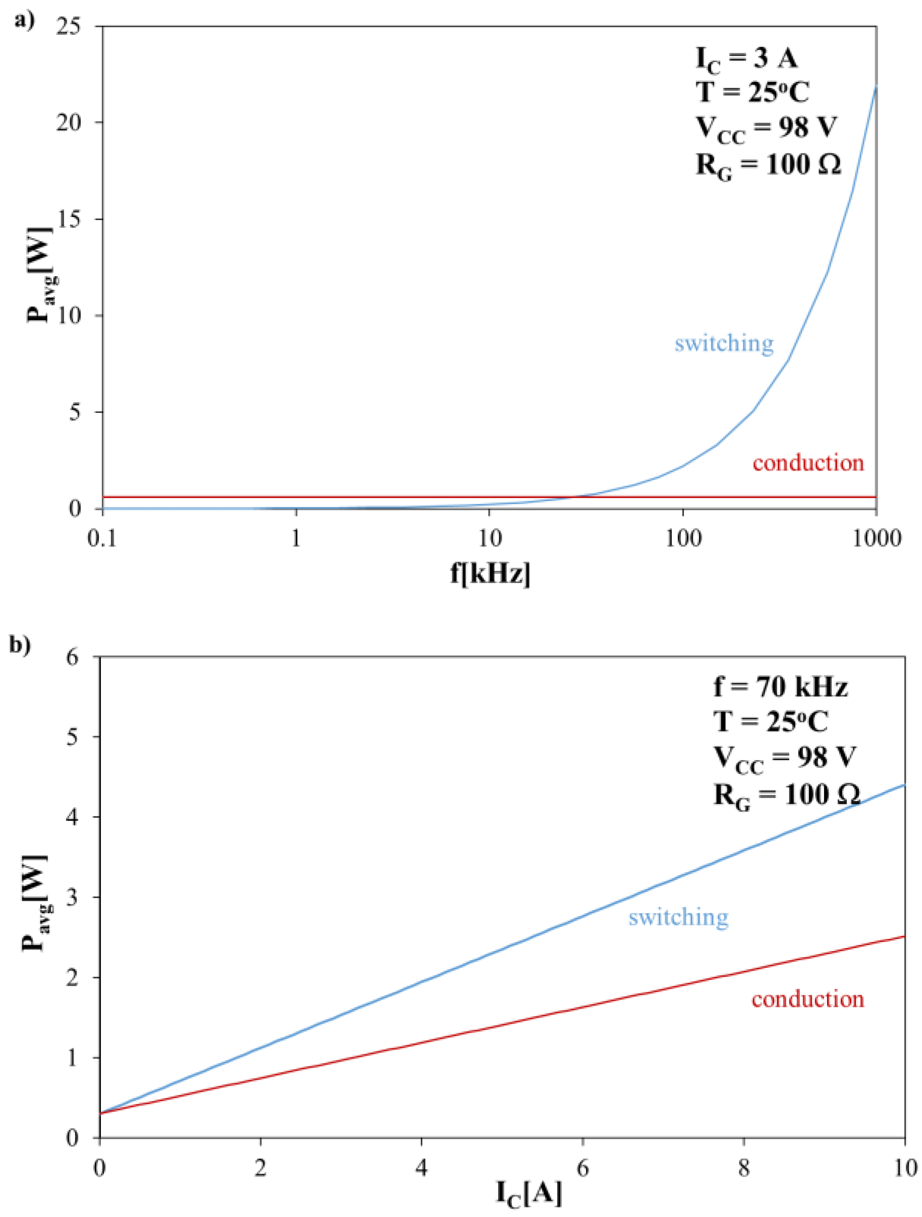
Figure 11, which show the conduction losses (red line) computed using the AVG model and the switching losses averaged for one period that are computed using the Formula (3)—blue line. The effect of frequency and the collector current on the average power dissipated in a transistor operating with resistive load is illustrated in
Figure 11a,b, respectively.
The curves shown in
Figure 11 show that both switching and conduction losses are an important component of the power dissipated in this device during its operation. It is particularly noteworthy that in
Figure 11 in the considered operating conditions, switching losses of the transistor are equal in the value to conduction losses for the frequency of 35 kHz, and for the frequency of 100 kHz, switching losses are already four times higher. It is also worth noting that in
Figure 11b, for the considered operating conditions, switching losses depend more strongly on the collector current than on conduction losses.
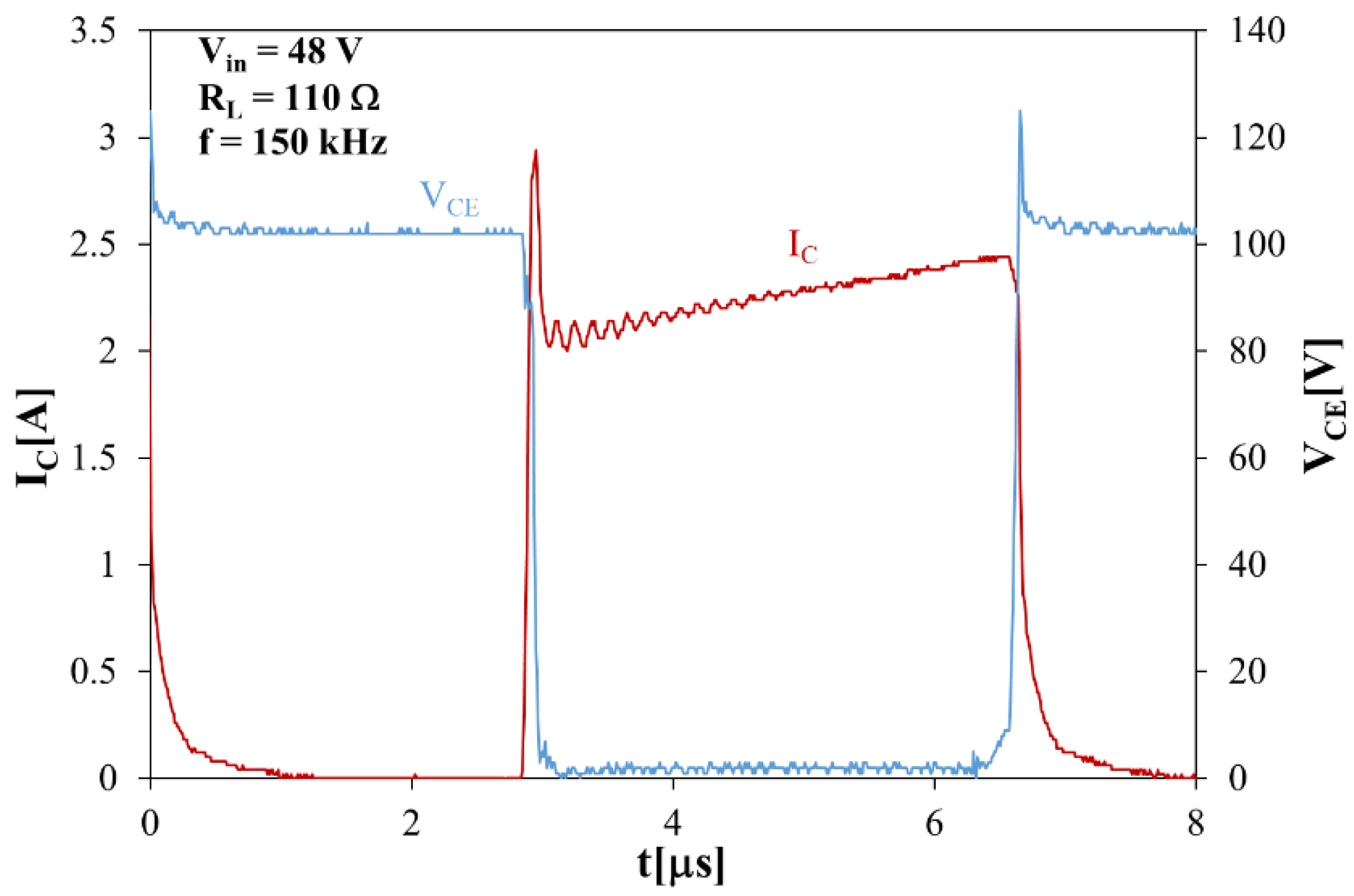
The discrepancy between the computation results taking into account the impact of the IGBT switching losses on its junction temperature and the measurement results shown in
Figure 11a probably results from not taking into account the influence of overvoltages and overcurrents on the value of turn-on and turn-off energies. Examples of overvoltages and overcurrents are shown in the waveforms shown in
Figure 12.
In the case of a diode, in the considered frequency range, switching losses are much lower than conduction losses [
38]. This is visible in
Figure 10b, on the basis of which it can be stated that when using the diode model that does not take into account the effect of losses associated with its switching, the value of its junction temperature is computed with good accuracy.
Minor discrepancies between the results of computations and measurements, which are presented in
Figure 9, result from inaccurate determination of the value of the duty cycle for the converter operating in the CCM. The problem of determining the value of the duty cycle is due to the fact that the operation of the IGBT with high switching frequency differs significantly from the operation of an ideal switch. In the case of an ideal switch, the value of the duty cycle voltage between the output terminals is equal to the value of the transistor control signal coefficient subtracted from one.
The computation method presented above was used in the formulas in the considered model. However, in the case of an IGBT operating with high switching frequency, due to non-zero values of parasitic capacitances, the value of the duty cycle of the signal between the output terminals of the transistor may significantly differ from the value for an ideal switch. In
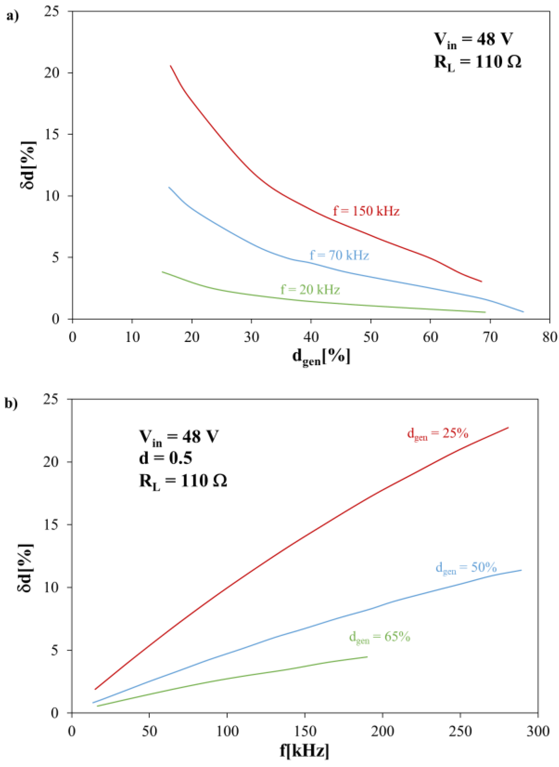
Figure 13, the dependences of the relative error in determining the duty cycle on the frequency of the control signal and the duty cycle of the control signal for the considered IGBT resulting from omitting the non-ideality of this device in determining this factor are presented. The value of this error was determined according to the formula
where d
GG is the value of the duty cycle of the signal at the output of the driver controlling the transistor, and d
VCE is the value of the duty cycle between the output terminals of the IGBT.
As it is presented in
Figure 10, for low control signal duty cycle values, the user has poor control over the actual voltage duty cycle value between the transistor output terminals. A similar effect can be observed with increasing frequency. This can lead to significant discrepancies between the computed value of the converter output voltage from the mathematical model and the one obtained during the measurements of the real converter.
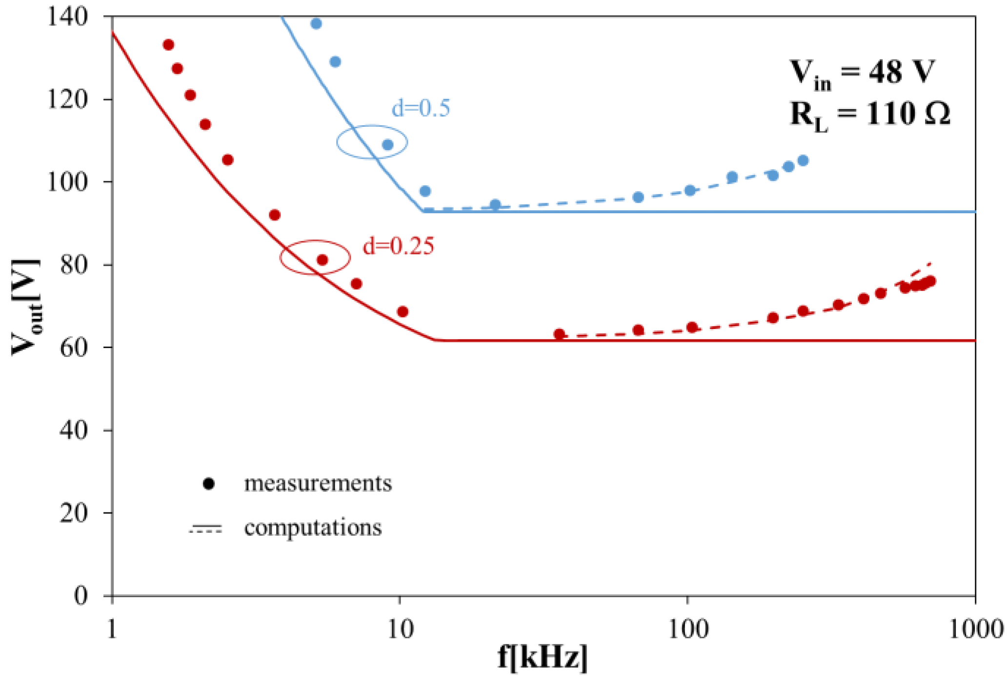
Figure 14 shows the dependence of the output voltage of the DC-DC converter on the switching frequency of the IGBT contained therein. In the figure, the computation results for the duty cycle value consistent with the signal at the driver output are marked using the solid line, and the dashed line is used for the V
out voltage values computed for the converter operating in the CCM taking into account the error in determining the duty cycle described above. In these computations, the dependence of the form is used:
where V
outc is the computed value of the output voltage using the model [
33], and ∆d is the absolute error in determining the duty cycle.
The converter output voltage dependencies presented in
Figure 14 prove that neglecting the influence of electrical inertia related to the switching of the IGBT leads to a value of the duty cycle of the collector–emitter voltage different than for the ideal switch. This is the reason why the error in determining the output voltage increases with increasing frequency. At the same time, as the computations show, taking this into account in computations allows for a significant improvement of its accuracy.
As indicated in the papers [
39,
40], the omission of the nonlinear dependence of thermal resistance of the IGBT junction temperature significantly influences the accuracy of determining the transistor junction temperature. In order to check whether this problem also occurs for the transistor operating in the boost converter, the measurements and computations of its output characteristics and the correlation between the interior temperature of the IGBT operating without a heat sink were carried out. In order to emphasise the considered issue,
Figure 15 presents only the measurement results for the converter operating in the CCM.
The results presented in
Figure 15 prove that even with the correct representation of electrical properties of the converter, i.e., losses related to switching the IGBT, the computed junction temperature value for high values of the output current is significantly overestimated due to the use of a linear thermal model in the AVG model. This problem could be solved relatively easily by averaging the nonlinear thermal model described in the paper [
39]. In the modified model, the thermal capacitances will be omitted, and one nonlinear resistor describing the dependence R
thj−a(T
j) will be used.
5. Conclusions
The paper presents the results of simulation and experimental studies illustrating the limitations of an electrothermal averaged model of a diode–transistor switch containing an IGBT and a rapid switching diode. The investigations were carried out for the boost converter in a wide range of changes of load current, frequency, and the duty cycle of the control signal. Various cooling conditions for the transistor and the diode contained in the tested converter were considered.
It was proved that for both the considered types of cooling conditions of semiconductor devices in the whole considered range of changes in the duty cycle and frequency of the control signal, good agreement was obtained between the computed and measured values of the output voltage of the boost converter operating in the CCM. On the other hand, in the DCM, the results of computations and measurements are convergent for the frequency f < 20 kHz and the load current Iout > 10 mA.
The problem of determining the value of the control signal duty cycle in the high-frequency range is pointed out. In this regard, the transistor switching times are not negligible in relation to the pulse duration. It was shown that at high frequency values f > 70 kHz, the error in determining the output voltage resulting from inaccuracy in determining the value of the duty cycle can reach even 10%. It is shown that this error could be reduced if the value of duty cycle is estimated, taking into account values of switch-on and switch-off times of the used transistor.
It is indicated that switching losses in the IGBT are significant for characteristics of the boost converter. It was shown that omitting these losses in the considered model causes significant, even twofold lowering of the value of the IGBT junction temperature increase above the ambient temperature. A modification of the description of the thermal model of the transistor using Formulas (5) and (6) was proposed to allow taking into account the influence of switching losses in the transistor on its junction temperature. It was shown that this modification allows improving the computation accuracy.
The problem of nonlinearity of thermal phenomena in semiconductor devices, which causes the junction temperature value to be overestimated in the range of high output currents of a converter, is also highlighted. The manner of taking into account the nonlinearity of the thermal model of the used semiconductor devices is proposed.
The problem of the junction temperature in the range of very low Iout values is also indicated. Improvement of the model under consideration that enables obtaining high accuracy of computations in a wide range of frequency changes will be the subject of further research by the authors.
The presented research results may be useful for designers of DC-DC converters. The presented results of computations and measurements also allow assessing the influence of the control signal frequency and load current as well as the cooling conditions of semiconductor devices on the properties of the tested boost converter.


