Abstract
Multi-level converters are widely used in various industrial applications. Among various space vector modulation (SVM) schemes, the multi-level SVM scheme based on two-level space vector pulse width modulation (SVPWM) is recognised as a simplified multi-level SVM scheme, which can reduce the computation complexity. However, this scheme is still complicated when the number of the voltage levels is large. This paper proposes a modified SVM scheme that can further simplify the multi-level SVM scheme based on two-level SVPWM. The proposed SVM scheme can directly determine the two-level hexagon where the reference voltage vector is located by calculating a simple formula. The whole modulation process can be completed by only three steps. Meanwhile, the proposed method is generic for any n-level converter without adding much calculation, which greatly simplifies the modulation process. Experimental results have been provided, which verify the effectiveness and generality of the proposed SVM scheme for two types of multi-level converters.
1. Introduction
Compared to the two-level converter, multi-level converters demonstrate clear advantages such as higher voltage operation capability, lower voltage stress (dv/dt), output harmonics and switching loss, higher efficiency, etc. [1,2,3]. However, there are also challenges associated with multi-level converters such as increased control and modulation complexity, the need for capacitor voltage balancing, reliability challenges, etc. [4], and this paper will focus on the modulation aspect.
Common multi-level space vector modulation (SVM) schemes can be classified into two typical categories: (1) carrier-based sinusoidal pulse width modulation (SPWM), including phase disposition PWM (PD-PWM) [5,6,7] and phase shifted PWM (PS-PWM) [8,9,10]; and (2) space vector PWM (SVPWM) [11]. With the appropriate zero-sequence signal injection, carrier based PWM is equivalent to SVPWM [12,13,14]. Both the two methods can achieve a high DC-link voltage utilization ratio, and the relationship between control objectives—such as neutral point voltage balancing and common mode voltage, and the space vectors and zero-sequence—can be well defined. Therefore, SPWM and SVPWM can have the same performance for multi-level converters. This paper mainly focuses on multi-level SVM.
For multi-level SVM, the research is mainly focused on two aspects: application and implementation. It is well known that multi-level SVM has redundant voltage space vectors, which have different effects on the multi-level converters. The converters can be controlled to output the required performance through selecting the appropriate voltage space vectors. Therefore, multi-level SVM has various applications, such as common-mode voltage reduction [15,16], harmonic suppression [17,18], balancing capacitor voltage [19], reducing switching losses [20], conferring fault tolerance [21], etc. Meanwhile, the multi-level SVM schemes can also be applied to some special multi-level converter topologies [22,23,24].
Although multi-level SVM has high flexibility, implementation is still challenging for the multi-level converters with more than three levels [25]. The conventional SVM is based on the α-β coordinate system. The modulation process includes complex sector judgement and trigonometric function operation. For a three-phase n-level system, the converter has n3 switching states and 6(n–1)2 triangles in total [26]. Due to plenty of triangles and voltage space vectors being involved, the conventional method is quite tedious to implement.
To simplify multi-level SVM implementation, many improved SVM schemes have been developed. One of the ideas is to use alternative coordinate transformations. The g-h coordinate system (60° space) [27] is a typical and fast method. In the g-h coordinate system, all coordinate components are transformed to integers, and it can quickly select the nearest three vectors and compute their duty cycles through simple calculation. Another method called the K-L coordinate system [11] is similar to the g-h coordinate system, and it is transformed into a 120° coordinate system. Other alternative coordinate transformations were proposed to implement multi-level SVM. For example, the imaginary coordinate system is defined as the line voltage and three axes of imaginary coordinates ja, jb and jc which are perpendicular to the three-phase axes a, b and c, respectively [28]. A generalized SVPWM coordinate system based on the convenient definition of three nonorthogonal static reference frames, alternative to the αβ coordinate system, was proposed in [29]. Moreover, these methods can be used in the multiphase multi-level converters [30,31].
Another idea to simplify multi-level SVM is based on the concept of two-level SVM [32]. It is well known that two-level SVM is very simple and easy to implement. Hence, the idea is to decompose Vref into a two-level hexagon and then implement the modulation based on two-level SVM. However, when the number of levels increases, determining the location of Vref among many two-level hexagons is very complex. Therefore, the key part of this kind of multi-level SVM is determining how to simply and accurately decompose Vref into the two-level hexagon.
There are several ways to decompose Vref. The well-known multi-level SVM scheme based on two-level SVPWM is the three-level to two-level SVM scheme [32]. This method is to divide the three-level space vector diagram into six two-level hexagons and then determine the two-level hexagon where Vref is located depending on its location. For a three-level converter, the principle of this algorithm is to divide the three-level space vector diagram into six two-level hexagons and then determine the two-level hexagon where Vref is located depending on its location. This method is simple to apply in the three-level converter. In [33], the scheme is initially applied in the five-level inverter. The implementation process is that the five-level space vector diagram should be divided into six three-level hexagons, and the three-level hexagons should first be determined. Then, each three-level hexagon is further divided into six two-level hexagons, and each two-level hexagon can be finally determined. Therefore, the decomposition by this method is layer by layer. It implies that as the number of levels increases, both the complexity and the computation increase. For determining the location of Vref, ref. [34] determines the two-level hexagons through identifying the triangle that encloses the tip of Vref.
Another idea to achieve the multi-level SVM scheme based on two-level SVPWM more quickly is proposed in [35]. In order to identify the center of the two-level hexagon where Vref is located, this method needs to calculate a “distance term” and compare for each vector on the inner side of a particular layer (the hexagonal ring where Vref is located). Therefore, the process of determining the two-hexagon has two steps. Step 1: identifying the layer. This step divides the space vector diagram into layers. For example, for a five-level converter, the space vector diagram can be viewed as being formed of four layers. The layer number where Vref is located should be obtained firstly. Step 2: generating candidate vectors for the two-level hexagon center. After identifying the layer, the distance of each vector on the inner side of the particular layer from Vref should be calculated and compared. The vector that is closest to Vref is chosen as the center of the two-level hexagon where Vref is located. However, when this algorithm is applied in converters with higher number of levels, the multiple comparisons still require significant computation resources.
For the multi-level SVM scheme based on two-level SVPWM, the problem is that the process of decomposing Vref is too complex and difficult to implement as the number of levels increases. In order to solve this issue, this paper proposes a new, generic, simplified multi-level SVM. This scheme can easily and effectively decompose Vref into the two-level hexagon, and the whole modulation process can be achieved by three simple steps. The proposed scheme has the following salient advantages compared with existing the methods mentioned above:
- (1)
- The center of the two-level hexagon where Vref is located can be directly expressed through a simple calculation. The decomposition does not require the layer calculations.
- (2)
- No lookup table or coordinate transformation are required.
- (3)
- For any n-level converter, the whole modulation process can be implemented within three-step calculations without adding much calculation, regardless of the number of levels.
The rest of this paper is organized as follows: Section 2 introduces the space vector diagram of the five-level converter and the coordinate normalization; Section 3 presents the proposed multi-level SVM scheme; Section 4 shows experimental results for two kinds of multi-level inverter, which validate the effectiveness of the proposed method; and Section 5 concludes the paper.
2. Space Voltage Vector Distribution
A five-level cascaded H-bridge inverter (CHB) as shown in Figure 1 is employed as an example for evaluation. Figure 2 shows the space vector diagram of the five-level converter.
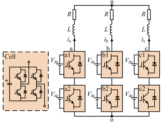
Figure 1.
The topology of the five-level cascaded H-bridge inverter.
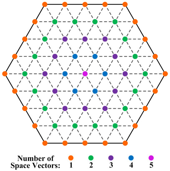
Figure 2.
The voltage space vector diagram of the five-level converter.
Figure 3 shows the coordinate components of the voltage space vectors in the a-b-c coordinate system. The coordinate components Va, Vb, Vc are per unit values after division by Vdc, and Vdc is the DC-link voltage of each cell. Then, the whole hexagon can be divided into six sectors (I–VI), as shown in Figure 3.
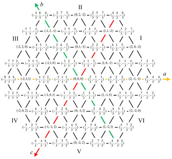
Figure 3.
The coordinate components of the voltage space vectors in the a-b-c coordinate system.
From Figure 3, it can be seen that the coordinate components of the voltage space vectors are symmetrically distributed in the six sectors. Therefore, in order to simplify the calculation process, the voltage space vectors in other sectors can be normalized to Sector I by interchanging the coordinate components [36]. Figure 4 shows the symmetry of the vector distributions (θ1 = θ2 = θ3 = θ4 = θ5 = θ6). The voltage space vectors in two adjacent sectors are symmetrically distributed with respect to the axis on which the two adjacent sectors coincide. For example, the voltage space vectors in Sectors I and II are symmetrically distributed with respect to the c-axis. Therefore, it is only necessary to interchange the coordinate components of the a-axis and b-axis to normalize the voltage space vectors of Sector II to Sector I, such as if the coordinate is (1/3, 4/3, −5/3) in Sector II, then the equivalent coordinate is (4/3, 1/3, −5/3) after normalizing it to Sector I. Similarly, the voltage space vectors in other sectors can also be normalized to Sector I according to this method. The equivalent coordinate components (Va1, Vb1, Vc1) of the voltage space vectors in Sector I are shown in Table 1. This coordinate normalization only needs to interchange the coordinate components and is easy to implement.
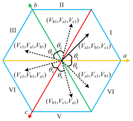
Figure 4.
The symmetry of the voltage space vector distributions.

Table 1.
Equivalent coordinate components of the voltage space vectors in Sector I.
3. Principle of the Proposed SVM Scheme
The proposed simplified multi-level SVM scheme only needs three steps to be completed. The whole modulation process is as follows.
- Step 1: Determining the Generalized Zero Vector
For the multi-level SVM scheme based on two-level SVPWM, the two-level hexagon where the reference voltage vector is located should be determined firstly, and this process is also the most important part. In this paper, the centers of the two-level hexagon are defined as the generalized zero vectors (GZV), as the red dots show in Figure 5.
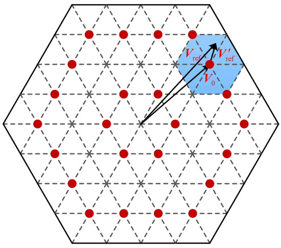
Figure 5.
The distribution of the generalized zero vectors for the five-level converter.
Sector I is analyzed as an example to show how to locate the GVZ, and there are six GVZs in total, as shown in Figure 6 (Point ①~⑥). In order to clearly locate the positions of GVZs, Sector I can be divided into six regions as shown by the dashed lines in Figure 6, denoted by different colors. The benefit of the idea of dividing into regions is that each region only has one GVZ, and the regions are not overlapping.
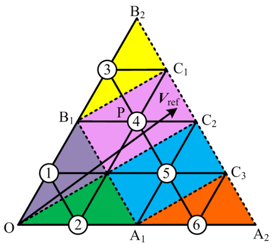
Figure 6.
Diagram of region partition in Sector I.
The expressions of the dashed lines can be obtained based on the coordinate components of the voltage space vectors shown in Figure 3 that are on the lines. The expressions are as follows:
B1C1 3Va1 + 3Vc1 = −2
OC2 3Va1 + 3Vc1 = 0
A1C3 3Va1 + 3Vc1 = 2
A1B1 Va1 − Vc1 = 2
A2B2 Va1 − Vc1 = 4
OC2 3Va1 + 3Vc1 = 0
A1C3 3Va1 + 3Vc1 = 2
A1B1 Va1 − Vc1 = 2
A2B2 Va1 − Vc1 = 4
Here, Vref in Region ④ is analyzed as an example, and the Point P is the GVZ in Region ④. In order to determine the location of the Point P, the intersection of the region borders should be firstly obtained. As shown in Figure 6, the Point C2 is the intersection of the borders of Region ④ (A2B2 and OC2). Therefore, the process of locating the GVZ (Point P) is shown in Figure 7, and the GVZ can be expressed as:
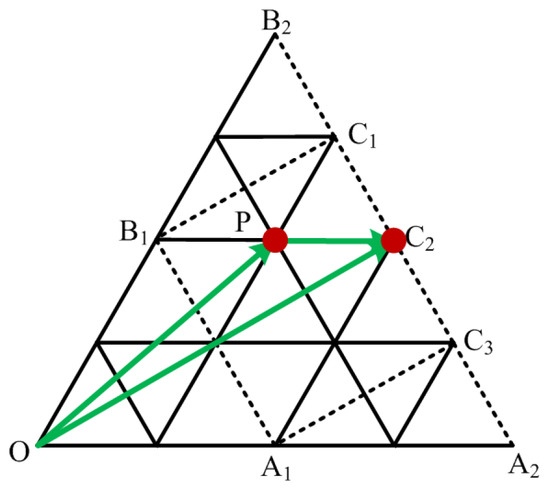
Figure 7.
The method of determining the GVZ.
As shown in Equation (2), the coordinates of the GVZ can be determined by subtracting the coordinates of the vector from the coordinates of the intersection (Point C2) of the region borders. In Figure 3, it can be seen that the voltage space vector has constant values (2/3, −1/3, −1/3), which is the shortest voltage space vector in the five-level converter. Hence, the only unknown in Equation (2) is the coordinates of , which should be obtained as follows.
Based on the characteristics of Equation (1), the common terms of all dashed lines are (3Va1 + 3Vc1, Va1 − Vc1), and all the constants are integers. Therefore, two variables x, y can be defined as in Equation (3) by using the coordinate components of Vref.
where (Va1_ref, Vb1_ref, Vc1_ref) are the equivalent coordinate components of Vref in Sector I, and the ceil (·) function means rounding up to the next larger integer. Based on the coordinate components of the voltage space vectors in Figure 3, the values of x, y corresponding to each region (where each GVZ ①–⑥ locates) can be summarized in Table 2.

Table 2.
The values of x and y corresponding to each region.
As shown in Table 2, x = 2 and y = 0 when Vref is in Region ④. Therefore, the coordinates (Va_C2, Vb_C2, Vc_C2) of the intersection (Point C2) of the region borders (A2B2 and OC2) can be expressed as
In Equation (4) are the expressions of A2B2 and OC2 by using the variables x and y, which are the same as in Equation (1). Then, based on (4) and Va_C2 + Vb_C2 + Vc_C2 = 0 (i.e., there is no zero-sequence component in a three-phase three-wire system), the coordinate components of Point C2 can be expressed by using x and y, as shown in Equation (5).
Finally, based on the Equation (2), the coordinate components (Va0, Vb0, Vc0) of the GVZ (Point P) can be expressed as
It can be seen that the coordinate components of all GVZs can be easily obtained by calculating Equation (6). According to the relationship of the multi-level space vector distribution, this SVM scheme can be extended to any n-level converter. Additionally, the variables x, y can be redefined as in Equation (7) to account for any n-level converter.
where the function rem (·) means the remainder of n/2, and n is the number of voltage levels. If n is odd, z = 1, and if n is even, z = 0. By adding the variable z, this simplified multi-level SVM scheme can be extended to any n-level converter without much increase in calculation.
According to the above analysis, Step 1, which is the most important part of the multi-level SVM scheme for determining the GVZs, can be easily achieved by calculating Equation (6). The process proposed here is much simpler than other SVM schemes based on two-level SVM in references [33,35] and does not require the layer calculations.
- Step 2: Space Vector State (Redundant Vector) Selection
For the SVM scheme, Vref is synthesized by the voltage space vectors around it. Therefore, it is necessary to select the most appropriate voltage space vectors.
For the multi-level converters, there are a large number of voltage space vectors, including redundant vectors. For a five-level converter, there are 125 voltage space vectors in total. The redundant voltage space vectors have different effects on the performance of the multi-level converters, such as reducing common-mode voltage [15,16], harmonic suppression [17,18], balancing capacitor voltage [19], reducing switching losses [20], conferring fault tolerance [21], etc. Therefore, the redundant voltage space vectors can be selected to achieve a certain objective. In this paper, common-mode voltage reduction is selected as the primary objective and is used as an example. The common-mode voltage can cause issues in motor drive systems, such as motor bearing damage, insulation breakdown and electromagnetic interface (EMI).
The common-mode voltage is different when different voltage space vectors are used. For a five-level converter, when all voltage space vectors are used, the common-mode voltages are ± 2Vdc, ±5Vdc/3, ±4Vdc/3, ±Vdc, ±2Vdc/3, ±Vdc/3, and 0, and the maximum common-mode voltage is ±2Vdc. Therefore, the common-mode voltage can be reduced by selecting the appropriate voltage space vectors. For example, the zero space vector at the origin in the space vector diagram in Figure 2 has five available vector states: (2 2 2), (1 1 1), (0 0 0), (−1 −1 −1) and (−2 −2 −2), and the corresponding common-mode voltages are 2Vdc, Vdc, 0, −Vdc and −2Vdc. Here, −2, −1, 0, 1 and 2 represent the five voltage levels in a five-level converter. The common-mode voltage is minimized when the middle voltage space vector state (0 0 0) is selected. Therefore, some voltage space vectors generating a larger common-mode voltage should not be used to reduce the common-mode voltage [15].
As shown in Figure 2, different points have different numbers of redundant voltage space vectors. When the point has an odd number of voltage space vectors, only the middle voltage space vector should be used. When the point has an even number of voltage space vectors, the middle two voltage space vectors should be used, as shown in Figure 8. At this point, the common-mode voltages are ±Vdc, ±2Vdc/3, ±Vdc/3 and 0, and the maximum common-mode voltage is ±Vdc, which is half of all voltage space vectors used.
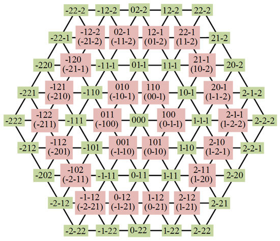
Figure 8.
The voltage space vectors to reduce the common-mode voltage for the five-level converter.
Based on Figure 5 or Figure 8, it can be seen that each GVZ has two voltage space vectors. Therefore, the initial space vector state should be determined at the beginning of the modulation cycle. The voltage space vectors within brackets are defined as the initial space vector states in Figure 8. For instance, when Vref is in Region ④ as shown in Figure 6, the initial space vector state is (1 0 –2), and the switching sequence is [(1 0 −2)-(2 0 −2)-(2 1 −2)-(2 1 −1)-(2 1 −2)-(2 0 −2)-(1 0 −2)].
The two voltage space vectors of each GVZ can be defined as Sup and Sdown. Sup is the starting vector state for the current cycle, Sdown is the ending vector state for the current cycle and also the starting space vector state of the next modulation cycle, and Sdown is defined as the initial space vector state. By analyzing the relationship between the values of x, y in Table 2 and the two voltage space vectors of the GVZs in Sector I in Figure 8, Sup and Sdown can be directly expressed by using the variables x and y as
Based on the above analysis, the initial space vector state can be directly expressed by using the variables x and y in Equation (8) when common-mode voltage reduction is the control objective. The main contribution of Step 2 is to reveal the relationship between the common-mode voltage reduction and the defined variables x and y, and it provides a theoretical approach to linking the common-mode reduction to the variables x and y.
When other control objectives need to be considered, such as harmonic (THD, WTHD) suppression, reducing switching losses, etc., in theory, the relationship between these control objectives and the variables x and y can also be determined based on the above-presented approach, and these control objectives have been implemented for many other SVPWM methods through selecting the redundant voltage space vectors [17,18,19,20,21]. The identification of these relationships needs to be further researched.
- Step 3: ON-Time Duration Based on Two-Level Simplified SVM
After decomposing Vref into the two-level hexagon, the ON-times of each phase can be calculated based on two-level SVM. The two-level equivalent reference voltage vector can be expressed as
where are the coordinate components of the two-level equivalent reference voltage vector , and (Va0, Vb0, Vc0) are the coordinate components of the GVZ.
Then, the ON-times of each phase can be calculated. Compared to conventional two-level SVM, two-level simplified SVM can directly calculate the ON-times through the three-phase reference voltage without judging the sector, calculating the ON-times of the basic space vectors and determining the switching sequence. The calculation can be greatly simplified [37]. Therefore, based on two-level simplified SVM, the ON-times of each phase can be directly expressed as
where Vavg = [max(Va′,Vb′,Vc′) + min(Va′,Vb′,Vc′)]/4, Ts is the switching cycle, and j = a, b, c. Therefore, Step 3 can be directly completed only through calculating the Equations (9) and (10).
After calculating the three steps (Equations (6), (8)–(10)), the proposed SVM scheme is complete when Vref is located in Sector I. Based on the coordinate normalization in Table 1, the coordinate components of the GVZs and the initial space vector Sdown (Sa0, Sb0, Sc0) in other sectors can be directly obtained through anti-normalization by interchanging the coordinate components. For example, the coordinate components of the GVZ and the initial space vector in Sector I are (Va0, Vb0, Vc0) and (x−1, −y, −x), respectively. If they are anti-normalized from Sector I to Sector II, it is only necessary to interchange the coordinate components of a-axis and b-axis, i.e., the coordinate components of the GVZ and the initial space vector are (Vb0, Va0, Vc0) and (−y, x−1, −x) in Sector II, respectively. The anti-normalization for the other sectors is the same, as shown in Table 3.

Table 3.
The anti-normalization of coordinate components of GVZs and initial voltage space vector states.
A flowchart of the proposed SVM scheme is shown in Figure 9. It shows the whole process of the proposed SVM schemes. By summarizing the above analysis, the normalization and anti-normalization only need to interchange the coordinate components without adding calculations. Therefore, the proposed SVM scheme only needs to calculate Steps 1, 2, and 3, and each step is only a simple mathematical calculation, which greatly simplifies the process of decomposing Vref. The whole modulation process does not require the layer calculations. Therefore, this SVM scheme can be extended to the higher level converters without adding much calculation.
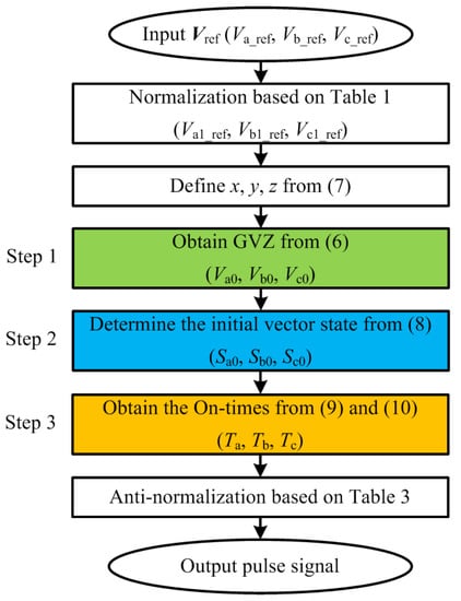
Figure 9.
Flowchart of the proposed space vector modulation (SVM) scheme.
4. Experimental Results
The proposed SVM scheme is validated on a three-phase five-level CHB inverter prototype. The experimental setup is shown in Figure 10. The power switches are insulated gate bipolar transistors (IGBT) (BSM50GB120DLC, 1200 V/50 A). The phase currents and voltages are measured by LEM voltage and current sensors (LA55-P and LV 25-P). The master controller board contains one DSP TMS320F28335 and one Xilinx Spartan3E FPGA XC3S500E. The whole SVM process is executed on the DSP, and the FPGA is only responsible for extending pulse signals. The experimental parameters are shown in Table 4.
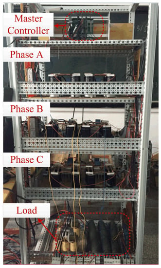
Figure 10.
Overview of the experimental five-level CHB setup.

Table 4.
Experimental parameters.
Here, the modulation index m is defined as
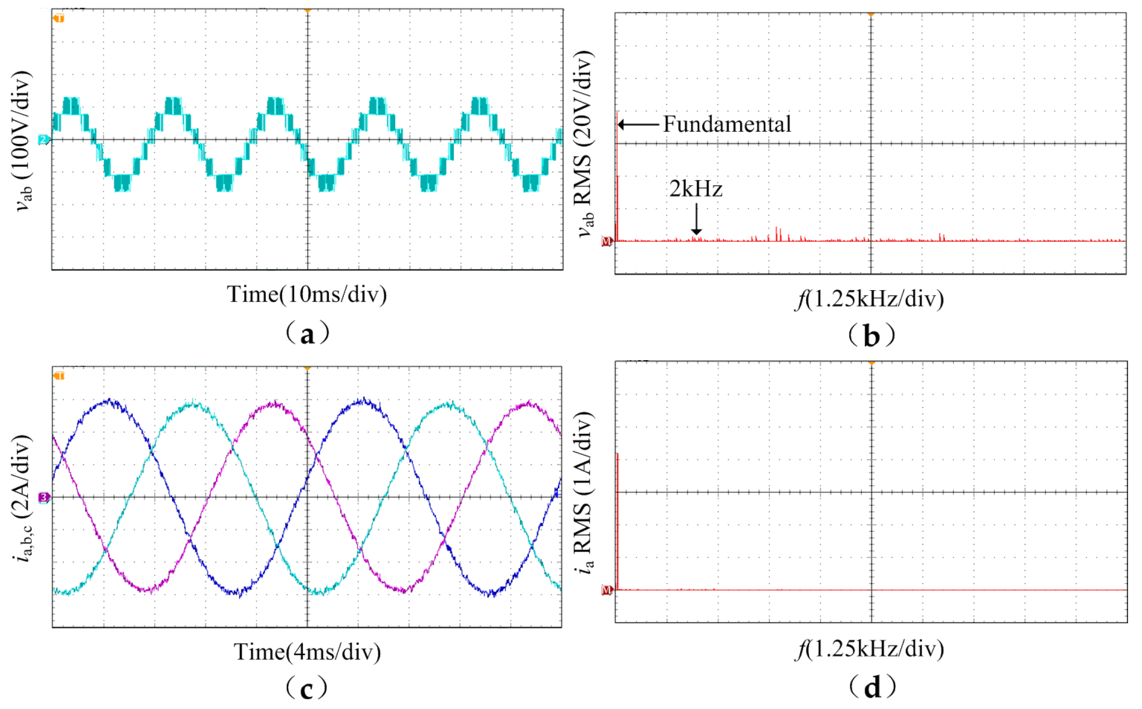
Figure 11 and Figure 12 show the performance of the proposed SVM scheme under different modulation indexes. Figure 13 shows the common-mode voltage waveform. Figure 11 shows the experimental results when m = 0.6. The line voltage vab has seven levels as expected, the total harmonic distortion (THD) is 23.46%, and the weight THD (WTHD) is 0.39%. Meanwhile, the harmonics of vab are mainly distributed around the integer multiples of the switching frequency of 2 kHz (nfs, n = 1, 2, 3, …). The three phase currents are highly sinusoidal, and the THD is 1.13%. Figure 12 shows the experimental results when m = 0.9. vab has nine levels as expected, the THD is 16.91%, and the WTHD is 0.27%. The three phase currents are also highly sinusoidal, and the THD is 0.8%. The line voltage in Figure 11 and Figure 12 contains a slight DC offset due to the DC bias of the voltage probe, which was not calibrated to zero. The main waveforms are correct as expected that the line voltage is seven levels when the modulation index is 0.6 and the line voltage is nine levels when the modulation index is 0.9. Meanwhile, the THD and WTHD of the proposed SVM scheme are very low, and the main components of the harmonics are switching frequency harmonics (around nfs). Therefore, the waveforms and THD results show that the proposed SVM scheme can ensure the converter can work properly with low harmonics. It should be noted that from the harmonics (THD) point of view, the proposed method has similar performance to other SVPWM methods. The focus of the proposed multi-level SVM scheme is not to reduce the THD but to reduce the computation time.
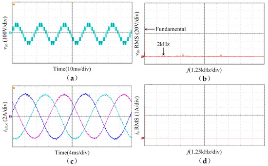
Figure 11.
Experimental results under m = 0.6: (a) line to line voltage; (b) Fast Fourier Transform (FFT) of the line to line voltage; (c) three phase currents; (d) FFT of the phase current.
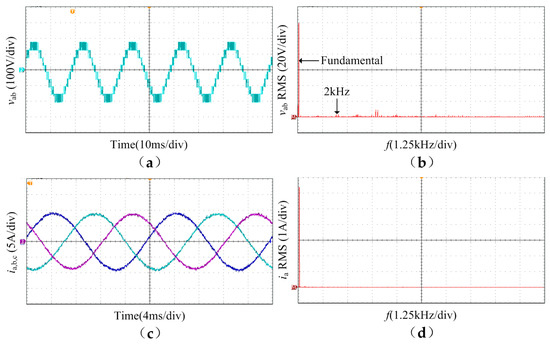
Figure 12.
Experimental results under m = 0.9: (a) line to line voltage; (b) FFT of the line to line voltage; (c) three phase currents; (d) FFT of the phase current.
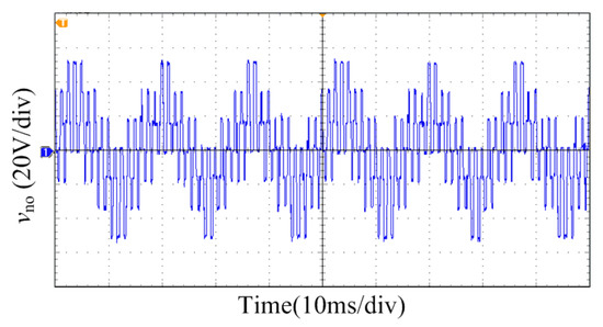
Figure 13.
The common-mode voltage waveform.
As shown in Figure 13, the common-mode voltage has seven values of ±Vdc, ±2Vdc/3, ±Vdc/3 and 0 in total, and the maximum common-mode voltage is Vdc = 50 V. It is consistent with the analysis in Step 2. Therefore, the selected voltage space vectors can effectively reduce the common-mode voltage, where the common-mode voltages ± 2Vdc, ±5Vdc/3 and ±4Vdc/3 have been removed.
The experimental results prove that the proposed SVM scheme can work well with low harmonics under different modulation indexes.
In order to verify the generality of the SVM scheme, another experimental validation is carried out on an existing four-level inverter [38] in the laboratory. The topology is shown in Figure 14. The four-level converter needs to control the flying capacitor (FC) voltages, and the control method has been given in [38]. For the four-level inverter, each output voltage level may correspond to multiple switching states. Therefore, before outputting the pulse signals, the converter needs to select the appropriate switching states according to the FC voltages. In other words, the FC voltage is controlled through choosing the appropriate (redundant) switching states within each phase leg, not through choosing the redundant space vectors in the three-phase SVPWM. Therefore, the modulation strategy only needs to be modified when the pulse signals are generated, to select the appropriate switching states for FC voltage control, as shown in Figure 15 (FC voltage control), and the three calculation steps of the proposed SVM scheme in the paper do not need to be changed. In order to accurately and objectively evaluate the SVM scheme for different multi-level converters, the computational time of the FC voltage control method is not counted when calculating the time for the four-level converter.
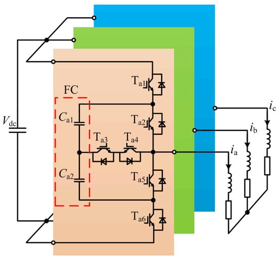
Figure 14.
The topology of the four-level inverter.
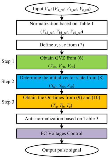
Figure 15.
The modulation strategy of the four-level inverter.
In order to verify the feasibility of the proposed scheme for the four-level converter, a down-scaled prototype is built in the laboratory. The controller of the prototype is based on a TI TMS320F28335 DSP and a Xilinx XC3S400 FPGA. The whole SVM scheme are also executed on the DSP, and the FPGA is responsible for extending pulse signals, as same as in the five-level CHB experimental validation. The phase currents and the FC voltages are measured by sensors from LEM (LA 55-P and LV 25-P). The power switches are IGBTs (IKW40N120T2 from Infineon, 1200 V/40 A). The experimental parameters are shown in Table 5.

Table 5.
Experimental parameters of the four-level converter.
The experimental results are shown in Figure 16. Figure 16 shows the line voltage, the three phase currents and the FC voltages when the modulation index is dynamically changed from 0.9 to 0.6. The comparison of the experimental results and theoretical results is shown in Table 6.
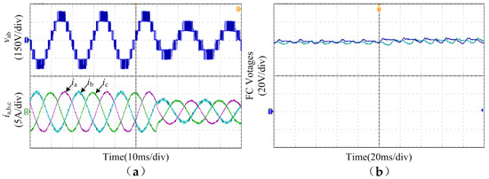
Figure 16.
Experimental results of the four-level inverter: (a) line to line voltage and three phase currents; (b) flying capacitor voltages.

Table 6.
Comparison of experimental results and theoretical results.
As shown in Figure 16, when the modulation index is 0.9, the waveform of the line voltage is seven voltage levels, as expected for theoretical analysis, and when the modulation index is 0.6, the waveform of the line voltage is five voltage levels, as expected for theoretical analysis. The three phase currents are highly sinusoidal, and all FC voltages can always be regulated near the desired value of Vdc/3 = 80 V. Meanwhile, as shown in Table 6, the experimental results for the four-level inverter are almost the same as the theoretical results. This proves that the proposed SVM scheme can also be used for the four-level converter and the converter can work normally.
The proposed SVM scheme is a simplified multi-level SVM scheme based on the two-level SVPWM. The main contribution is that the scheme greatly simplifies the process of decomposing Vref, and the whole modulation process does not require the layer calculations. In order to evaluate the efficiency of the proposed SVM scheme, a comparison with an existing same type of SVM is necessary. The well-known and representative multi-level SVMs based on two-level SVPWM are described in [33,35]. Therefore, the computational times of three SVM schemes (the proposed SVM and the SVM schemes based on two-level SVM in [33,35]) were measured and compared in the DSP, as shown in Figure 17.
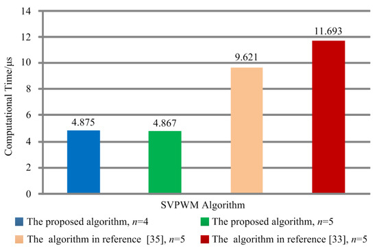
Figure 17.
Computational times of the three SVM schemes in the DSP.
It can be seen that the computational time of the proposed SVM scheme is less than that of the two SVM schemes in [33,35]. Meanwhile, the computational times are slightly different for the four-level and five-level converters with the proposed SVM method. The reason is that the variables x and y are calculated differently in four-level and five-level SVM. Based on the Equation (7), when the voltage level is even, x and y are expressed as
When the voltage level is odd, the variables x and y are expressed as Equation (3), which is slightly different to in Equation (12). Therefore, the computational time of the four-level SVM is slightly more than the computational time of the five-level SVM.
For a three-level converter, the computational time of the algorithm in [33] is 5.713 μs and the computational time of the algorithm in [35] is 5.207 μs. It is shown that the two methods are relatively simple for a three-level converter, but the computational time of the two methods in [33,35] increases as the number of voltage levels increases due to the layer calculations, as shown in Figure 17. However, no matter how many the voltage levels there are, the process of the proposed algorithm is the same as shown in the flowchart in Figure 9. The whole modulation only needs to calculate Equations (6), (8)–(10). The only difference is that expressions of the variables x and y are different for the odd- and even-level converters. Therefore, for any odd-level converter, the computational time of the proposed SVM scheme is the same according to the Equation (3). For any even-level converter, the computational time is also the same according to the Equation (12). Both of them are almost the same, as shown in Figure 17 (the blue one and the green one). The comparison proves that the proposed SVM scheme greatly simplifies the modulation process of the multi-level SVM scheme based on two-level SVPWM and can be expanded to any n-level converter, and the computational times are almost the same.
5. Conclusions
In order to solve the issue that the multi-level SVM scheme is difficult to implement, this paper proposes a generic simplified multi-level SVM scheme based on the two-level SVM scheme. Compared to the existing multi-level SVM schemes based on the two-level SVM scheme, the proposed SVM scheme does not require a lookup table, coordinate transformation or layer calculations. The whole modulation process can be completed by only three steps, and each step only needs to calculate simple mathematical equations, which greatly simplifies the process of decomposing Vref. The whole modulation scheme is easy to implement. For any odd-level converter, the computational time of the proposed SVM scheme is the same, as is so for any even-level converter, and both of these times are almost the same. Therefore, the proposed SVM scheme can be used for any n-level converter without adding much calculation, regardless of the number of levels. Common-mode voltage reduction is selected as the primary objective and is used as an example, and the common-mode voltage can be reduced by half. Meanwhile, the proposed SVM scheme reveals the relationship between the common-mode voltage reduction and the switching sequence, and provides a theoretical approach to linking the common-mode reduction to the initial space vector states. When other control objectives are considered, the relationships between these control objectives and the switching sequence can also be determined based on the presented theoretical approach. In order to verify the feasibility and generality of the proposed SVM scheme, the experimental results for the four-level and five-level converters are provided. The experimental results prove that the proposed SVM scheme can ensure that the two types of converter work normally and that the computation effort does not increase with number of levels, so it can be readily applied to any n-level converter. Meanwhile, the proposed SVM scheme is more efficient than other multi-level SVM schemes based on two-level SVPWM, which greatly simplifies the modulation process.
Author Contributions
C.W. wrote the paper, analyzed the principle and designed the experiments; X.Y. shared his experience and knowledge in advanced multilevel converter; Y.Z. analyzed the simulation data; X.W. helped to perform the analysis with constructive discussions. All authors have read and agreed to the published version of the manuscript.
Funding
This research was funded by joint Ph.D. program of “double first rate” construction disciplines of CUMT.
Conflicts of Interest
The authors declare no conflict of interest.
References
- Kouro, S.; Malinowski, M.; Gopakunmar, K.; Pou, J.; Franquelo, L.G.; Wu, B.; Rodriguez, J.; Pérez, M.A.; Leon, J.I. Recent advances and industrial applications of multilevel converters. IEEE Trans. Ind. Electron. 2010, 57, 2553–2580. [Google Scholar] [CrossRef]
- Yuan, X. Derivation of voltage source multilevel converter topologies. IEEE Trans. Ind. Electron. 2017, 64, 966–976. [Google Scholar] [CrossRef]
- Norambuena, M.; Kouro, S.; Dieckerhoff, S.; Rodriguez, J. Reduced multilevel converter: A novel multilevel converter with a reduced number of active switches. IEEE Trans. Ind. Electron. 2018, 65, 3636–3645. [Google Scholar] [CrossRef]
- Franquelo, L.G.; Rodriguez, J.; Leon, J.I.; Kouro, S.; Portillo, R.; Prats, M.A.M. The age of multilevel converters arrives. IEEE Ind. Electron. Mag. 2008, 2, 28–39. [Google Scholar] [CrossRef]
- Lim, Z.; Maswood, A.I.; Ooi, G.H.P. Common-mode reduction for ANPC with enhanced harmonic profile using interleaved sawtooth carrier phase-disposition PWM. IEEE Trans. Ind. Electron. 2016, 63, 7887–7897. [Google Scholar] [CrossRef]
- Deng, F.; Yu, Q.; Wang, Q.; Zhu, R.; Cai, X.; Chen, Z. Suppression of DC-link current ripple for modular multilevel converters under phase-disposition PWM. IEEE Trans. Power Electron. 2020, 35, 3310–3324. [Google Scholar] [CrossRef]
- Paris, J.M.D.; Osorio, C.R.D.; Pinheiro, H.; Carnielutti, F.D.M. Phase disposition modulation with sorting algorithm for symmetrical cascaded multilevel converters. IEEE Trans. Ind. Appl. 2019, 55, 7527–7536. [Google Scholar] [CrossRef]
- Sahoo, S.K.; Bhattacharya, T. Phase-shifted carrier-based synchronized sinusoidal PWM techniques for a cascaded H-bridge multilevel inverter. IEEE Trans. Power Electron. 2018, 33, 513–524. [Google Scholar] [CrossRef]
- Tan, B.; Gu, Z.; Shen, K.; Ding, X. Third harmonic injection SPWM method based on alternating carrier polarity to suppress the common mode voltage. IEEE Access 2019, 7, 9805–9816. [Google Scholar] [CrossRef]
- Zhu, W.; Chen, C.; Duan, S.; Wang, T.; Liu, P. A carrier-based discontinuous PWM method with varying clamped area for vienna rectifier. IEEE Trans. Ind. Electron. 2019, 66, 7177–7188. [Google Scholar] [CrossRef]
- Attique, Q.M.; Li, Y.; Wang, K. A survey on space-vector pulse width modulation for multilevel inverters. CPSS Trans. Power Electron. Appl. 2017, 2, 226–236. [Google Scholar] [CrossRef]
- Zhou, K.; Wang, D. Relationship between space-vector modulation and three-phase carrier-based PWM: A comprehensive analysis. IEEE Trans. Ind. Electron. 2002, 49, 186–196. [Google Scholar] [CrossRef]
- Yuan, X.; Li, Y.; Wang, C. Objective optimisation for multilevel neutral-point-clamped converters with zero-sequence signal control. IET Power Electron. 2010, 3, 755–763. [Google Scholar] [CrossRef]
- Wang, J.; Gao, Y.; Jiang, W. A carrier-based implementation of virtual space vector modulation for neutral-point-clamped three-level inverter. IEEE Trans. Ind. Electron. 2017, 64, 9580–9586. [Google Scholar] [CrossRef]
- Renge, M.M.; Suryawanshi, H.M. Three-dimensional space-vector modulation to reduce common-mode voltage for multilevel inverter. IEEE Trans. Ind. Electron. 2010, 57, 2324–2331. [Google Scholar] [CrossRef]
- Zhang, X.; Wu, X.; Geng, C.; Ping, X.; Chen, S.; Zhang, H. An improved simplified PWM for three-level neutral point clamped inverter based on two-level common-mode voltage reduction PWM. IEEE Trans. Power Electron. 2020. (Early Access). [Google Scholar] [CrossRef]
- Gu, M.; Ogasawara, S.; Takemoto, M. Novel PWM schemes with multi SVPWM of sensorless IPMSM drives for reducing current ripple. IEEE Trans. Power Electron. 2016, 31, 6461–6475. [Google Scholar] [CrossRef]
- Gao, Z.; Ge, Q.; Li, Y.; Zhao, L.; Zhang, B. A SVPWM method with reduced switching frequency suitable for high power three-NPC rectifiers. In Proceedings of the IEEE Energy Conversion Congress and Exposition (ECCE), Baltimore, MD, USA, 29 September–3 October 2019; pp. 4824–4831. [Google Scholar]
- Lin, H.; Shu, Z.; He, X.; Liu, M. N-D SVPWM with DC voltage balancing and vector smooth transition algorithm for a cascaded multilevel converter. IEEE Trans. Ind. Electron. 2018, 65, 3837–3847. [Google Scholar] [CrossRef]
- Oghorada, O.J.K.; Zhang, L.; Efika, I.B.; Nwobu, C.J. Control of modular multilevel converters using an overlapping multihexagon space vector modulation scheme. IEEE J. Emerg. Sel. Top. Power Electron. 2019, 7, 381–391. [Google Scholar] [CrossRef]
- Li, X.; Dusmez, S.; Akin, B.; Rajashekara, K. A new active fault-tolerant SVPWM strategy for single-phase faults in three-phase multilevel converters. IEEE Trans. Ind. Electron. 2015, 62, 3955–3965. [Google Scholar] [CrossRef]
- Li, J.; Jiang, J.; Qiao, S. A space vector pulse width modulation for five-level nested neutral point piloted converter. IEEE Trans. Power Electron. 2017, 32, 5991–6004. [Google Scholar] [CrossRef]
- Xu, H.; Yao, W.; Shao, S. Improved SVPWM schemes for Vienna rectifiers without current distortion. In Proceedings of the IEEE Energy Conversion Congress and Exposition (ECCE), Cincinnati, OH, USA, 1–5 October 2017; pp. 3410–3414. [Google Scholar]
- Tan, L.; Wu, B.; Sood, V.; Xu, D.; Narimani, M.; Cheng, Z.; Zargari, N.R. A simplified space vector modulation for four-level nested neutral-point clamped inverters with complete control of flying-capacitor voltages. IEEE Trans. Power Electron. 2018, 33, 1997–2006. [Google Scholar] [CrossRef]
- Madasamy, P.; Pongiannan, R.K.; Ravichandran, S.; Padmanaban, S.; Chokkalingam, B.; Hossain, E.; Adedayo, Y. A simple multilevel space vector modulation technique and MATLAB system generator built FPGA implementation for three-level neutral-point clamped inverter. Energies 2019, 12, 4332. [Google Scholar] [CrossRef]
- Ahmed, I.; Borghate, V.B.; Matsa, A.; Meshram, P.M.; Suryawanshi, H.M.; Chaudhari, M.A. Simplified space vector modulation techniques for multilevel inverter. IEEE Trans. Power Electron. 2016, 31, 8483–8499. [Google Scholar] [CrossRef]
- Celanovic, N.; Boroyevich, D. A fast space vector modulation algorithm for multilevel three-phase converters. IEEE Trans. Ind. Appl. 2001, 37, 637–641. [Google Scholar] [CrossRef]
- Li, Y.; Gao, Y.; Hou, X. A general SVM algorithm for multilevel converters considering zero-sequence component control. In Proceedings of the 31st Annual Conference of IEEE Industrial Electronics Society (IECON), Raleigh, NC, USA, 6–10 November 2005; pp. 508–513. [Google Scholar]
- Ovalle, A.; Hernandez, M.E.; Ramos, G.A. A flexible nonorthogonal-reference-frame-based SVPWM framework for multilevel inverters. IEEE Trans. Power Electron. 2017, 32, 4925–4938. [Google Scholar] [CrossRef]
- Sakthisudhursun, B.; Pandit, J.K.; Aware, M.V. Simplified three-level five-phase SVPWM. IEEE Trans. Power Electron. 2016, 31, 2429–2436. [Google Scholar] [CrossRef]
- Pu, T.; Bu, F.; Xu, H.; Huang, W. Dual-frequency discontinuous space vector pulse width modulation for five-phase voltage source inverter with harmonic injection. CSEE J. Power Energy Syst. 2019. (Early Access). [Google Scholar]
- Seo, J.H.; Choi, C.H.; Hyun, D.S. A new simplified space-vector PWM method for three-level inverters. IEEE Trans. Power Electron. 2001, 16, 545–550. [Google Scholar]
- Lalili, D.; Lourci, N.; Berkouk, E.M.; Boudjema, F.; Petzoldt, J.; Dali, M.Y. A simplified space vector pulse width modulation algorithm for five level diode clamping inverter. In Proceedings of the International Symposium on Power Electronics, Electrical Drives, Automation and Motion (SPEEDAM), Taormina, Italy, 23–26 May 2006; pp. 1321–1326. [Google Scholar]
- Gupta, A.K.; Khambadkone, A.M. A space vector PWM scheme for multilevel inverters based on two-level space vector PWM. IEEE Trans. Ind. Electron. 2006, 53, 1631–1639. [Google Scholar] [CrossRef]
- Aneesh, M.A.S.; Gopinath, A.; Baiju, M.R. A simple space vector PWM generation scheme for any general n-level inverter. IEEE Trans. Ind. Electron. 2009, 56, 1649–1659. [Google Scholar]
- Pou, J.; Rodriguez, P.; Boroyevich, D.; Pindado, R.; Candela, I. Efficient space-vector modulation algorithm for multilevel converters with low switching frequencies in the devices. In Proceedings of the IEEE 36th Power Electronics Specialists Conference, Recife, Brazil, 16 June 2005; pp. 2521–2526. [Google Scholar]
- Bakhshai, A.; Joos, G.; Espinoza, J.; Jin, H. Fast space vector modulation based on a neurocomputing digital signal processor. In Proceedings of the APEC 97-Applied Power Electronics Conference, Atlanta, GA, USA, 27 February 1997; pp. 872–878. [Google Scholar]
- Wei, C.; Yuan, X.; Zhou, J.; Wang, K.; Zhang, Y.; Wu, X. Voltage jump suppression and capacitor voltage fluctuation analysis for a four-level hybrid flying capacitor T-type converter. Energies 2019, 12, 698. [Google Scholar] [CrossRef]
© 2020 by the authors. Licensee MDPI, Basel, Switzerland. This article is an open access article distributed under the terms and conditions of the Creative Commons Attribution (CC BY) license (http://creativecommons.org/licenses/by/4.0/).


