Article

Control Design and Experimental Validation of a HB-NPC as a Shunt Active Power Filter

by
Gerardo Escobar
1,
Panfilo R. Martinez-Rodriguez
2,*,
Samuel Iturriaga-Medina
2,
Gerardo Vazquez-Guzman
3,
Jose M. Sosa-Zuñiga
3 and
Diego Langarica-Cordoba
2
1
Tecnologico de Monterrey, Nuevo Leon 64849, Mexico
2
School of Sciences, Universidad Autonoma de San Luis Potosi (UASLP), San Luis Potosi 78295, SLP, Mexico
3
Laboratory of Electrical Engineering and Power Electronics, Instituto Tecnologico Superior de Irapuato (ITESI), Km 12.5 Carr. Irapuato-Silao 36821, GTO, Mexico
*
Author to whom correspondence should be addressed.
Energies 2020, 13(7), 1691; https://doi.org/10.3390/en13071691
Submission received: 12 January 2020 / Revised: 17 February 2020 / Accepted: 1 March 2020 / Published: 3 April 2020

Abstract

:
This work presents the design of a control law based on the average model of a shunt active power filter considering an H-bridge neutral point clamped topology and its experimental validation. Therefore, the proposed controller is formed by three control loops, namely current (inner), regulation (outer), and balance control loops. The current loop aims to compensate both the displacement power factor and the harmonic distortion produced by nonlinear loads connected to the point of common coupling. To deal with harmonic current distortion, the current loop involves an adaptive mechanism based on a bank of resonant filters tuned at odd harmonics of the fundamental grid frequency. The regulation and balance loops are aimed to maintain the voltage of the capacitors forming the DC-link at a desired constant level. For this, proportional-integral controllers are designed. The design of all three loops considers the average model of the system. The performance of the proposed multi-loop control law is evaluated through numerical results and real-time experimental implementation, both considering a 2 kW academic benchmark with a constant switching frequency of 7 kHz. In order to provide harmonic distortion, a nonlinear load based on an uncontrolled diode bridge rectifier is considered. Additionally, step-load changes from 0.5 kW to 1 kW are considered for the nonlinear load. As a result, a suitable current tracking, voltage regulation, and balance are observed despite parametric uncertainties, load variations, and harmonic distortion. As a consequence, in steady state, simulation results indicate that the compensated grid current THD is 1.75%; meanwhile, the nonlinear load current THD is 52.5%. Experimental results indicate that the compensated grid current THD is 2.32%; meanwhile, the nonlinear load current THD is 53.8%.

1. Introduction

The ever increasing connection of non-linear loads (NLL) to the grid has produced power quality problems in sensitive electrical distribution systems. In particular, these NLL enlarge the reactive power and harmonic components circulating in electrical grids, which, in turn, lead to several issues, such as voltage waveform distortions, overheating of distribution transformers, electromagnetic interference, and inefficient distribution of energy, among others. Currently, modern electrical systems are adopting the concept of smart grids, which allows dealing in a more appropriate way with the high penetration of renewable energy (solar, wind, biomass energy, etc.) and multiple electronic loads. However, the need for energy quality compensators is still imperative [1]. Shunt active power filters (SAPF) represent a viable alternative to attenuate the adverse effects caused by NLL [2,3]. SAPF can compensate both the harmonics generated by NLL and the reactive power produced by non-resistive linear loads to ensure a power factor (PF) close to unity according to international power quality standards, such as IEEE-519 [4]. Therefore, the use of SAPF entails a significant increase in the overall efficiency of the system and leads to reduced energy consumption costs.
The typical structure of an SAPF consists of a voltage source inverter (VSI), which converts the type of electrical energy and serves as a coupling between the grid and the DC-link. The DC-link in the SAPF is made of capacitors, large enough to store energy to compensate transient current peaks throughout the operation of the system. An output filter is generally used as the coupling impedance between the VSI and the grid at the point of common coupling (PCC) to reduce the current switching ripple. Many VSI topologies used in SAPF applications have been studied. In particular, multilevel converters have demonstrated better characteristics when compared to traditional two-level conventional topologies [2]. Mainly, multilevel inverters are able to produce higher quality voltage and current waveforms. Furthermore, in multilevel inverters, the voltage across the switching devices is lower, which implies low electric stress on power semiconductors and a reduction of switching losses, keeping high efficiency. For instance, the five level HB-NPC topology has shown efficiency greater than 96 % for photovoltaic applications [5].
In particular, the neutral point clamped (NPC) [6,7,8], full H-bridge [9], and flying capacitor [10], which are three-level power converter topologies, have been used as the VSI in SAPF applications. Five-level inverters, namely five-level (one-leg) NPC [11,12], H-bridge NPC (HB-NPC) [13,14], and cascade full-bridge topologies [15], have also been used as SAPF. Five-level inverters are able to generate an AC output voltage waveform with smaller switching ripple as compared to three-level inverters. They also provide lower common-mode voltage, lower harmonic distortion, and lower electromagnetic interference [6,16,17]. For instance, in [18], a cascade H-bridge (CHB) based multilevel converter was used as a static VAR compensator (STATCOM) in a wind farm. Additionally, a CHB-based SAPF using single-phase toroidal core transformers in cascaded configuration was presented in [19], which allowed the system to operate with a single DC-link capacitor. Furthermore, a detailed comparison of multilevel topologies’ characteristics and their applications were presented in [20,21].
In the last few years, research related to the control design for different topologies used in SAPF applications has been carried out extensively as well. For instance, the work in [8] presented a control design for a three-level NPC as an SAPF. Here, the control method aimed to solve the current tracking problem and provided damping to the three order output filter. In [11,12], fuzzy logic control solutions were presented to solve the current tracking problem in a five-level NPC converter. In [22], a three-phase VSI connected to the PCC was used as an SAPF. In this case, the NLL was represented by an electric vehicle supplied by a photovoltaic system, which was controlled by a neuro-fuzzy inference system in combination with an MPPT scheme. In [23], a combination of a neural network control strategy plus a bandless hysteresis controller was proposed for a switched capacitor used as an SAPF. However, due to the nonlinear nature of the system, this control technique produced variable switching frequency, leading to undesirable resonance effects in grid-tied power electronics converters [24]. In [25], a proportional-integral (PI) iterative controller was proposed for a shunt hybrid power filter. In [26], a modified multifrequency passivity-based control (PBC) strategy was proposed for an SAPF based on a T-Type inverter topology. The modification consisted of the introduction of a PI regulator into the coupling loop of the conventional PBC. In [3], a model-based sliding-mode control (SMC) was proposed for a three-phase full-bridge shunt active power filter. The solution consisted of a Kalman filter structure to estimate the variables used to generate the switching surfaces. Nevertheless, a major drawback of SMC is the oscillations, also referred to as chattering, which are produced due to the switching time delay and the unknown dynamics of the system. As a consequence, SMC presents low control precision and unstable switching frequency in power electronics applications interacting with the electrical grid [27].
However, multilevel inverters exhibit also certain drawbacks. For instance, the control design becomes more challenging than in conventional three-level topologies. In fact, most multilevel power converters require an extra control strategy to guarantee that each capacitor in the topology maintains a specific voltage level. This is referred to as the voltage balancing loop, which gets more involved for higher levels and may represent a considerable additional computational cost. For instance, the work in [28] described in detail the modeling and control design for a three-level half-bridge NPC converter used as an SAPF, whereas, in [29], a control scheme for the cascaded H-bridge topology was proposed. In [30], a predictive current control scheme for an SAPF was presented. In [13,14], also predictive current control schemes were proposed for single-phase NPC power converters as an SAPF. In [14], a single-objective predictive control method was proposed for a single-phase SAPF based on a three-level NPC converter. Here, the control scheme aimed to compensate the reactive power and harmonic distortion without using weighting factors as the cost function. In [10], a novel finite control state set model predictive control was proposed for a flying capacitor topology operating as an SAPF. However, an issue for the implementation of predictive control techniques is the tuning for a reliable weighting factor, which is a complex optimization challenge in active power filtering applications [14]. Moreover, the absence of a modulating signal produces a varying switching frequency due to the limited number of valid switching states generating large current and voltage ripples [31].
This paper presents the modeling process and control design of an SAPF based on a five-level HB-NPC topology. This topology is composed of the bridge connection of two NPC branches, which provides five output voltage levels. The controller includes a control law capable of compensating reactive and harmonic currents. As the DC-link is split and composed of two capacitors, the controller also includes two additional voltage loops, namely voltage balance and regulation control loops to control the DC-link.
The contributions of this work towards shunt active power filtering are as follows:
  • The design of a multi-loop controller for SAPF based on a five-level HB-NPC topology, which considers a time scale separation between current and voltage dynamics. The last yields three independent control loops, i.e., current tracking loop, voltage regulation loop, and voltage balance loop for PF correction and harmonic mitigation.
  • The proposed control scheme does not depend on system parameters’ knowledge; therefore, a robust behavior against grid uncertain parameters, output filter uncertain parameters, current harmonic distortion, and load variations is exhibited.
  • According to the best of the authors knowledge, there is no similar work in the literature regarding the experimental validation of the proposed control scheme applied to a five-level HB-NPC topology for an SAPF of 2 kW academic prototype with a constant switching frequency of 7 kHz.
The rest of the paper is organized as follows: In Section 2, the model of the system is obtained, and the control objectives together with the main assumptions are presented. Section 3 details the design of the three control loops, and numerical results are presented as well. Section 4.2 shows experimental results to evaluate the performance of the closed-loop system. Finally, Section 5 provides some concluding remarks about the present work.

2. System Description

Figure 1 depicts the five-level HB-NPC (5L-HB-NPC) topology used as an SAPF, which is connected in parallel to the NLL. The grid voltage is represented by v G , which supplies both the NLL and the SAPF, and has a fundamental frequency given by ω . The grid impedance is represented by the series connection of L G and R G . Hence, the voltage at the PCC is given by:
v PCC = v G L G i ˙ G R G i G .
The SAPF is coupled to the PCC through an L F filter ( R F represents the filter parasitic resistance). Notice that, to generate a multilevel output voltage, it is necessary to store enough energy in both DC-link capacitors C 1 and C 2 . In other words, it is necessary to maintain a DC-link voltage level high enough to allow the reconstruction of a required VSI output voltage, also referred to as the injected voltage. The VSI output voltage must dominate the grid voltage amplitude to allow the appropriate injection of current towards the grid. Moreover, it is mandatory to guarantee that all capacitors in the DC-bus have a balanced voltage to avoid asymmetries on the reconstructed injected voltage. This fact will be detailed later in the control objectives’ definition.
As shown in Figure 1, the 5L-HB-NPC consists of two branches of conventional three-level NPC converters connected in an H-bridge configuration. Every switch of the topology is represented by S n ( n { 1 , 2 , 3 , 4 , 5 , 6 , 7 , 8 } ). The topology involves four diodes to gain access from the mid-point of the DC-link to the VSI output voltage to produce the null states. The permissible outputs for the converter are summarized in Table 1, where the value o one represents the ON state, whilst the value of zero represents the OFF state at the corresponding switch. The inverter output voltage is represented by e A F , which takes values from a discrete set of possible voltage levels, i.e., e A F { v C 1 , v C 2 , ( v C 1 + v C 2 ) , 0 , ( v C 1 + v C 2 ) , v C 1 , v C 2 } .
To simplify the modeling process, an equivalent circuit that represents a simplification of the power converter operation is obtained following the guidelines presented in [32] and is shown in Figure 2, where the switches are replaced by two equivalent single pole triple throw switches. Notice that δ 1 and δ 2 represent switching functions taking values in the discrete set { 1 , 0 , 1 } . Table 1 relates the switch positions combinations to the equivalent switching functions δ 1 and δ 2 . Out of this equivalence, the following expression of the control signal e A F in terms of the switching functions δ 1 and δ 2 and the DC capacitor voltage levels can be obtained:
e A F = 1 2 ( δ 1 δ 2 ) ( v C 1 + v C 2 ) + 1 2 ( δ 1 2 δ 2 2 ) ( v C 1 v C 2 ) .
As stated in the power electronics literature [33], the model SAPF based on the 5L-HB-NPC can be obtained by direct application of Kirchhoff’s current and voltage laws, on the equivalent circuit of Figure 2, which yields:
( L F + L G ) x ˙ G = ( R G + R F ) x G e A F + L F i ˙ NLL + R F i NLL + v G ,
C x ˙ R = u a ( x G i NLL ) x R R ,
C x ˙ B = u a u b ( x G i NLL ) x B R ,
e A F = x R u a 2 + x B u a u b 2 ,
u a = Δ δ 1 δ 2 ,
u b = Δ δ 1 + δ 2 ,
where x G = Δ i G , x R = Δ ( v C 1 + v C 2 ) , and x B = Δ ( v C 1 v C 2 ) . The nonlinear current generated by the NLL is represented by i NLL . Notice that the state x R provides a measure of the capacitor voltage regulation, while the state x B represents the capacitor voltage difference at the DC-link, i.e., the voltage balance. The output inductive filter is represented by L F . The DC-link is formed by two bulky capacitors C 1 and C 2 with the same capacitance value, i.e., C 1 = C 2 = C. Notice that the resistive term R is considered a system parameter and represents the typical resistance used for safety reasons to discharge the DC-link capacitors in maintenance works [34]. Notice also that this resistor is commonly of a high value above tens of kilo ohms and may provide a small damping effect on the system. On the other hand, the voltage at the PCC v PCC is an available signal to be measured.
For control design purposes, an average model of the system is considered instead. For this, the switching signals δ 1 and δ 2 are replaced by the corresponding duty ratios d 1 and d 2 , which abide by the continuous range [ 1 , 1 ] . That is, in the above model, only the definitions of u a and u b are modified as follows:
u a = Δ d 1 d 2 , u b = Δ d 1 + d 2 .
which, in principle, makes e A F a continuous signal and smooths the dynamics of all three states x G , x R , and x B . Notice that the duty cycles can be recovered from (9) as follows:
d 1 = 1 2 ( u a + u b ) , d 2 = 1 2 ( u b u a ) .
The usage of averaged models for control design is a widely-accepted practice and is supported by the fact that the switching frequency of the power converter is at least 10 times higher than the bandwidth of the closed-loop system dynamics.
Based on the system model (3)–(8), the following three control objectives can be stated, namely current tracking, voltage balance, and voltage regulation objectives:
O1.
Current tracking objective: An inner (current) control loop is designed to guarantee tracking of the state x G towards a desired reference x G * , i.e., (Without loss of generality, time dependency is only explicitly used in (11) and (13)–(15). Throughout the paper, time dependency is omitted for simplicity.):
lim t x G ( t ) = x G * ( t ) ,
where the current reference is calculated as:
x G * = p v PCC , RMS 2 v PCC , 1 ,
where v PCC , 1 is the fundamental component of v PCC and v PCC , RMS its RMS value. In practice, v PCC may be polluted by harmonic distortion, and thus, it is preferred to construct the current reference x G ( t ) in terms of the fundamental component. Signal v PCC , 1 can be obtained from an external filter or with a phase-locked loop (PLL) scheme [35]. The term p represents the active power reference of the system, which modulates the amplitude of the grid current. The scalar term p is obtained from the outer (regulation voltage) control loop, as will be explained later.
O2.
Voltage regulation objective: An outer (regulation voltage) loop is designed to maintain (on average) the DC-link voltage regulated to a desired constant value V DC . In particular, this control objective is expressed as:
lim t x R 0 ( t ) = V DC ,
where x R 0 represents the DC component of x R and is used to address the average of x R , which is extracted using the following averaging function:
x R 0 ( t ) = 1 T t T t x R ( τ ) d τ ,
where T represents the fundamental period of the disturbance signal; in this case, a second order harmonic of the fundamental is expected, and thus, T = π / ω can be proposed.
As an outcome of this control loop, the power reference p is obtained. The regulation objective must guarantee that the DC-Link stores enough energy to allow the appropriate injection of the compensating (reactive and harmonic) current to the PCC.
O3.
Voltage balance objective: A balance loop is designed to guarantee that capacitors C 1 and C 2 , in the DC-bus, achieve the same voltage level. This avoids asymmetries on the reconstructed injected voltage and guarantees a safe operation of the capacitors. Equivalently, the balance objective is reached if the difference of the capacitor voltages x B goes to zero, that is,
lim t x B ( t ) = 0 .
Additional to the control objectives above defined, the following assumptions are formulated based on the physical construction of the system. These assumption allow, in principle, decoupling the model of the system into three separated dynamics, which permits a simplified analysis and design of the control scheme and establishing the parameter tuning rules.
A1.
The inductor current dynamics is faster than the voltage dynamics (in the closed loop). Furthermore, the voltage balance dynamics is considered faster than the voltage regulation dynamics (in the closed loop). Hence, the controller design procedure can be divided into three independent loops’ design (one loop for each dynamics). This is commonly referred to as the decoupling assumption and is based on the singular perturbation theory and analysis [36], i.e., a time scale separation.
A2.
The fundamental frequency of the grid voltage ω = 2 π f G is a known constant.
A3.
The i NLL , as well as the v PCC are periodic signals (may be perturbed by harmonic disturbances) with a fundamental frequency ω , and thus, they can be described by Fourier series as follows:
v PCC = h H G Ψ h V P , h , i NLL = h H G Ψ h I N L , h ,
Ψ h = cos h ω t sin h ω t , V P , h = V P , h r V P , h i ,
I N L , h = I N L , h r I N L , h i ,
where V P , h and I N L , h are the vectors of unknown harmonic coefficients. Normally, for single-phase systems, such a harmonic distortion is only comprised of odd harmonics, i.e., harmonics in the set H G = { 1 , 3 , 5 , } .
A4.
The system parameters L F , C, and R are considered positive unknown constants or may vary slowly due to the aging effect.

3. Controller Design

Based on Assumption A1, the system can be split into three dynamics, each accompanied by its corresponding controller design. The design is thus performed in three separated loops referred to as the current tracking loop, voltage balance loop, and voltage regulation loop, which are explained in detail next.

3.1. Current Tracking Loop

The system current dynamics is described by Subsystem (3), where signal e A F has become a continuous signal after the averaging argumentation, i.e., after replacing the switching signals δ 1 and δ 2 by the corresponding duty ratios d 1 and d 2 , as above explained
The new e A F can be seen as a filtered version of the generated VSI output voltage. However, e A F represents the actual control input of Subsystem (3), and thus, it becomes the reference voltage to be reconstructed by the VSI.
Notice that e A F in (6) is comprised of two terms. First is the term ε A F = x R u a / 2 , which is designed to solve the current tracking issue, i.e., to produce the appropriate injected current. Second is the term x B u a u b / 2 , which is a vanishing term, i.e., it equals zero in the steady state after the voltage balance is reached.
Rewriting the current dynamics (3) in terms of the increments yields the following system referred to as the error model:
( L F + L G ) x ˜ ˙ G = R P x ˜ G ε A F + ϕ H x B u a u b 2 L G x ˙ G * R P x G * + v G ,
ε A F = x R u a / 2 ,
where x ˜ G = Δ ( x G x G * ) is the error (or increment) of the grid current, i.e., the feedback state; ε A F is the non-vanishing part of e A F ; the term x B u a u b 2 is considered as a vanishing perturbation; R P = Δ R F + R G is an unknown positive lumping the parasitic resistances of the system; and ϕ H is a term where periodic signals are collected as follows:
ϕ H = L F i ˙ NLL + R F i NLL + L F x ˙ G * R F x G * .
Subsequently, based on Assumption A3, the term ϕ H contains similar harmonic contents as the NLL.
Based on the error model (16) and the periodic properties of term ϕ H above described, the following control law is proposed:
ε A F = v PCC + k C x ˜ G + ϕ ^ H .
The proposed control law in (18) is comprised of three terms. First, a feedforward term v PCC is added to alleviate the exogenous perturbation produced by the effect of the grid impedance. Second, a proportional term, associated with proportional gain k C > 0 , is included to add damping to the system. Third, a harmonic compensation term ϕ ^ H is included to cope with the harmonic term ϕ H considered as a perturbation. The design of this latter follows the ideas in [34], which appealed to the internal model principle [37].
Subsystem (16) in the closed loop with the proposed control law (18) yields the following error model:
L F x ˜ ˙ G = ( k C + R P ) x ˜ G + ϕ ˜ H x B u a u b 2 ,
where ϕ ˜ H is designed as described in [34], which consists of a bank of second-order harmonic oscillators, i.e., a bank of resonant filters tuned at odd harmonics of the fundamental frequency. The control law (18) can be written as:
ε A F = v PCC + k C x ˜ G + h H G 2 λ h s s 2 + h 2 ω h 2 x ˜ G ,
where λ h > 0 is the gain of the h-th oscillator tuned at the h ω -th harmonic.
Notice that the design of the current tracking loop neglects the vanishing perturbation x B u a u b / 2 appearing in (16). This is based on the fact that the balance loop, to be described next, guarantees x B 0 , while u a and u b are bounded by construction and relatively small, and thus, the product yields a relatively small amount.
Based on the structure of (17), it is proposed to calculate the auxiliary control variable u a , which is necessary to recuperate the duty cycles d 1 and d 2 according to (10), as follows:
u a = 2 ε A F x R .

3.2. Regulation and Balance Control Loops

The design of the voltage balance and regulation loops appeals to the decoupling Assumption A1. This is guaranteed if a suitable design of the physical system and selection of the adequate control parameters is performed. As a consequence, the current dynamics reach the steady state faster than the rest of the system. Therefore, it is assumed that x G = x G * in a relatively short time, which means that x ˜ G = 0 and ε A F = v PCC .

3.2.1. Voltage Balance Control Loop

The design of the voltage balance loop considers Subsystem (5) evaluated at the steady state value of the control input (21) above described and subject to the restriction x G = x G * . The dynamics of the voltage balance can thus be rewritten as follows:
C x ˙ B = 2 u b x R p P L x 3 R .
This is a first-order system (22) with control input u b affected by a constant term. The term p = Δ x G * v PCC 0 is calculated at the regulation loop to be explained later, while the term i NLL v PCC = Δ P L represents the load consumed power. Hence, the power term ( p P L ) coincides with the power losses of the system collected in the term R, i.e., p P L 2 V DC 2 / R . In fact, a more convenient representation for (22) is the following:
C x ˙ B = u b 4 V DC R x 3 R .
Based on the structure of (23), the following control law is proposed to guarantee voltage balance. It consists of a proportional plus an integral controller:
u b = ( k p B x B + k i B χ B )
χ ˙ B = x B ,
where k p B is a proportional gain and k i B is an integral gain of the proposed PI controller; χ B is an auxiliary variable to realize the integral part.
The auxiliary control signal u b together with u a above calculated in the current tracking loop are necessary to recuperate the duty cycles d 1 and d 2 according to (10).

3.2.2. Voltage Regulation Control Loop

The voltage regulation loop aims to guarantee that the DC-link is charged to a desired V DC voltage level well above the grid voltage peak value. This is a necessary condition to allow proper compensation of harmonic distortion and reactive power, as above explained. The design of the voltage regulation control loop considers Subsystem (4). The decoupling assumption A1 is also considered, out of which the control signal ε A F in (18) has reached its steady state value. Therefore, the voltage regulation dynamics are simplified as follows:
C z ˙ R = 2 v PCC ( x G * i L ) 2 z R R ,
where the following transformation to the new state variable z R has been used:
z R = Δ x R 2 2 .
After this variable transformation, the voltage regulation objective (O2) changes to guarantee regulation of the new variable z R towards a desired reference V DC 2 2 . Expressing Subsystem (26) in terms of increments of the new variable z R yields the following system:
C 2 z ˜ ˙ R = p P L z ˜ R R ,
where the error z ˜ R is defined as:
z ˜ R = Δ z R V DC 2 2 ,
and the term p is used only to consider the DC component of the product x G * v PCC , that is p = Δ x G * v PCC 0 . Notice that p acts as the control input in the system (28).
Based on the structure of the system (28), the following modified PI control law is proposed to guarantee voltage regulation (on average):
p = ( k i R ζ R + k p R χ R ) , ζ ˙ R = z ˜ R , τ R χ ˙ R = z ˜ R χ R ,
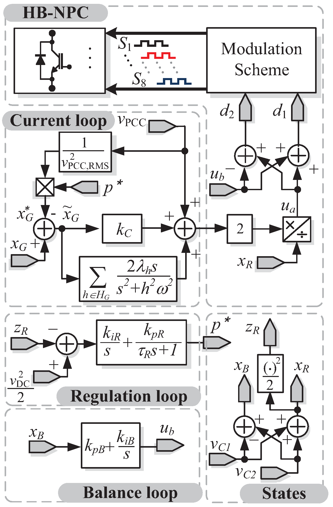
where k p R > 0 is the proportional gain and k i R > 0 is the integral gain. Notice that, in the proposed modified PI controller (29), the proportional term includes a first-order low-pass filter with a time constant given by τ R . This modification of the PI controller avoids the reinjection of the ripple present in z R towards p . The block diagram of the overall proposed scheme is presented in Figure 3. Notice that the resulting control scheme makes use of two PI controller at voltage loops in combination with a proportional plus a bank of resonant filters at the current loop. The overall scheme can be easily implemented in a digital signal processor.

3.3. Tuning Guidelines

In what follows, tuning rules for the parameters of the proposed controller are presented to guarantee a desired closed-loop performance. These guidelines are based on the average model of the system, the control objectives, and the assumptions for the controller design.

3.3.1. Tuning Guidelines: Current Tracking Loop

As mentioned above, to guarantee the stability of the current tracking loop and the convergence of the tracking error x G to zero, it suffices to select k C > 0 . However, to guarantee certain performance, it is still necessary to find certain boundaries as described next.
Consider the closed-loop dynamics of the current subsystem (19), which can also be expressed as:
L F x ˜ ˙ G + k C x ˜ G = ϕ ˜ H ,
where ϕ ˜ H = Δ ϕ ^ H ϕ H represents the harmonic disturbance estimation error. Note that the bandwidth of (30) is given by ω B W x G = k C / L F . Thereby, if ω B W x G is limited to be at most 1 / 10 of the sampling frequency 2 π f s , then k C must fulfill:
k C π L F f s 5 .

3.3.2. Tuning Guidelines: Voltage Balance Loop

The tuning of parameters k p B and k i B of the voltage balance loop is based on Subsystem (22), which can be rewritten as follows:
C x ˙ B = 4 V DC R ( k p B x B + k i B χ B ) x 3 R .
Its characteristic polynomial is given by:
P B ( s ) = s 2 + 2 k p B + 1 R C s + 2 k i B R C .
For this second-order system, the natural oscillation frequency and the damping factor are given by:
ω n B = 2 k i B R C ,
χ = 2 k p B + 1 2 k i B R C .
By assuming that ω R C 10 and considering a critically damped response, then parameters k p B and k i B can be tuned according to:
k i B ω 2 R C 50 , k p B 2 2 ω R C 10 .

3.3.3. Tuning Guidelines: Voltage Regulation Loop

The tuning of k p R , k i R , and τ R considers the closed-loop subsystem (29), which can be rewritten as:
C 2 z ˜ ˙ R = k p R χ R k i R ζ R z R R V DC 2 2 , ζ ˙ R = z ˜ R , τ R χ R = z ˜ R χ R ,
where ζ R is a state variable associated with the integral action and χ R is the state associated with the LPFmodification. It is a common practice to select τ R 1 / ( 2 ω ) , where ω is the fundamental frequency. Hence, the effect of the pole located at 1 / τ R can be neglected from Subsystem (37), which is then reduced to a second order system. The characteristic polynomial of this reduced system is given by:
P R ( s ) = s 2 + 2 k p R + 2 R C s + 2 k i R R C ,
where the damping factor and the natural oscillation frequency can be obtained as:
ς = R k p R + 1 R k i R C ,
ω n R = 2 k i R C .
If the damping factor is restricted to ς 1 / 2 , then the bandwidth dynamics of the voltage regulation must comply with ω B W x R ω n R . Furthermore, in agreement with the time-scale separation assumption, the condition ω B W x R ω B W x G must hold. Moreover, to avoid the effect of the second harmonic fluctuation, ω x R can be further restricted to ω / 5 . Thus, the parameters can be selected according to:
k i R ω 2 C 10 , k p R ω C 200 ,
where it has been assumed that ω R C 20 .

4. Numerical and Experimental Results

In this section, numerical and experimental results are given in order to assess the performance of the proposed control law. For the experimental results, R F , L G , and R G were unknown parameters. However, the controller was capable of dealing with these uncertainties.

4.1. Numerical Results

Numerical simulation results considering the system of Figure 4 are displayed in this part. For this purpose, PSCAD software was employed. The system parameters of the SAPF are shown in Table 2, and the controller parameters are depicted in Table 3.
The steady state responses of the voltage at the PCC v PCC , the grid current i G , the current demanded by the NLL i NLL , and the current injected by the SAPF i A F are shown in Figure 5. Notice that, despite the load current i NLL being highly distorted, the proposed control law was able to compensate the grid current i G to the desired sinusoidal waveform and in phase with the voltage at PCC v PCC ; where i A F is the quadrature current provided by the SAPF to compensate the nonlinear current i NLL . Note also that the THD of i G had a value of 1.75%, while the current consumed by the NLL i NLL presented a THD of 52.5%.
Figure 6 shows the steady state responses of the voltage v PCC , the fundamental component of the voltage at the PCC v PCC , 1 , the compensated current i G , and the VSI output voltage e A F . At this point, it is worth mentioning that the grid current i G was constructed using the fundamental component of the grid voltage v PCC , 1 to avoid the harmonics re-injection through the current reference of the current control loop. The computation of the current reference using v PCC , 1 guaranteed that the proposed control law was able to compensate the grid current i G to a sinusoidal signal and in phase with the grid voltage v PCC . Notice that v PCC , 1 was obtained by using a band-pass filter as in [28] or by using an extra phase-locked loop algorithm [35]. The five-level output voltage of the multilevel converter e A F is also shown in this figure.
The transient responses of the voltage across each capacitor of the DC-Link v C 1 , v C 2 , the sum of the capacitors voltage x R , and the power reference calculated in the regulation loop p * during a step change in the NLL are presented in Figure 7. It can be noted that during the change in the power demand, the voltage regulation loop was capable of maintaining the voltage on each capacitor of the DC-Link v C 1 , v C 2 at the desired value of 110 V each, after a smooth transient. Moreover, in Figure 8, it is possible to observe that the difference between v C 1 and v C 2 was zero on average, which demonstrated the effectiveness of the voltage balance loop facing the changes in the power demand. Furthermore, the current tracking loop exhibited a smooth waveform transition during the power demand, increasing or decreasing the amplitude of i G as required.
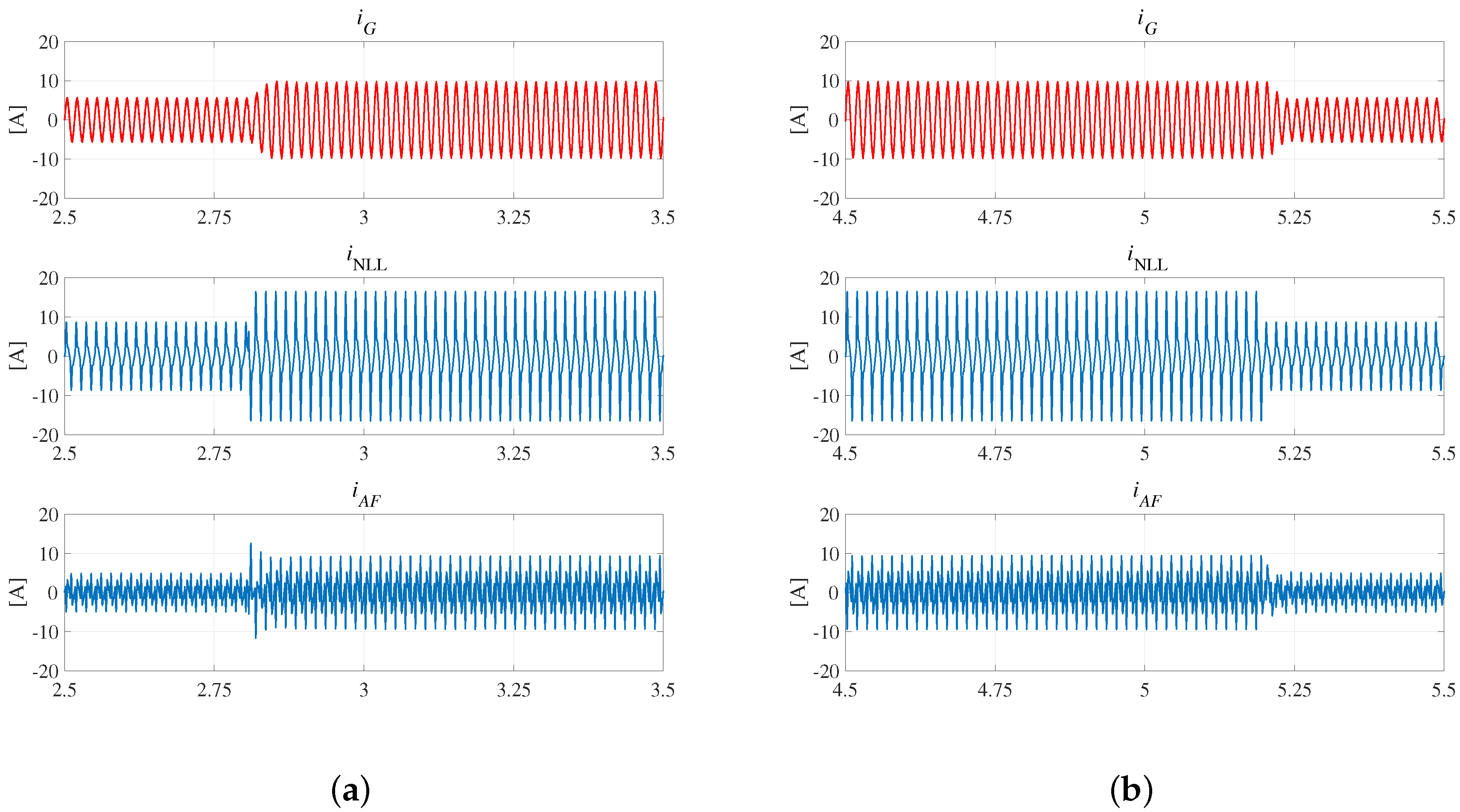
Figure 9 shows the transient responses of the grid current i G , the current consumed by the NLL i NLL , and the current injected from the SAPF i A F during a change of power at the NLL. Note that the waveforms of i G and i A F did not present any undesirable overshoot during the load changes.
In order to further evaluate the performance of the proposed control law, an RLload connected to the output of the uncontrolled bridge rectifier was considered for evaluation. In this case and only for this numerical evaluation case, the electrical NLL consisted of a single-phase uncontrolled rectifier (NLL-H in Figure 4) with R L 2 = 100 Ω , R N L 2 = 15 Ω and L L 2 = 12 mH, considering two different sizes of inductive output filters L F = 2 mH in Figure 10a and was reduced to L F = 1 mH in Figure 10b. Therefore, in Figure 10a, the steady state responses of the voltage at the point of common coupling v PCC , the grid current i G , the current demanded by the NLL i NLL , and the current injected by the SAPF i A F are presented. Despite the connection of a different NLL, the controller was capable of achieving an almost sinusoidal current i G . Nevertheless, a slight deviation appeared as small peaks during the load current zero-crossing on the compensated grid current i G . This fact occurred given that the slope of NLL was close to 90o, which was produced by the bulky inductance of NLL, and the size of the output filter helped to eliminate the switching frequency, conversely limiting the current compensation capacity in pronounced slopes. Note that the current deformation was able to be alleviated if a small output inductance was placed as in Figure 10b, but the switching ripple increased. Notice also that the total compensation of this spike was not possible given the well-known limitations imposed by the output filter ( Δ i A F / Δ t ). On the other hand, the grid current i G was in phase with the voltage at the PCC v PCC in both cases, which proved the benefits of the controller for power quality improvement despite the NLL loads connected at the PCC. For Figure 10a, the THD of the compensated grid current i G was 1.49 % ; meanwhile, for NLL current i NLL , the THD was 17.1 % . On the other hand, for the compensated grid current i G of Figure 10b, the THD was 1.1 % ; meanwhile, the THD of the NLL i NLL stayed at the same value of 17.1 % . Notice that the THD of the compensated grid current i G in both cases reached values less than 5 % .

4.2. Experimental Results

The performance of the SAPF based on the 5L-HB-NPC inverter under the proposed controller was experimentally tested in a 2 kW prototype with a constant switching frequency of 7 kHz. The 5L-HB-NPC as an SAPF was implemented as shown in Figure 4. The system parameters for the academic prototype are summarized in Table 2. As depicted in Figure 4, the SAPF was connected to the PCC to compensate the nonlinear currents produced by the NLL. The i NLL was produced by a pair of NLLs, which were implemented as uncontrolled diode bridge rectifiers feeding an RCload composed of a resistor R N L n , a capacitor C N L n , and an input inductance L L n . Furthermore, a linear resistor R L n was connected at the input of each NLL to increment the power demand. The combination of these load produced a distorted current referred as i NLL to be compensated by the SAPF. Notice that n = 1 , 2 was used to refer to the fixed low nonlinear load (NLL-L) or the switched high nonlinear load (NLL-H). The system parameters of the SAPF are summarized in Table 2. The SAPF was implemented using the discrete semiconductors IRG4PC40FD as IGBT switching elements and the semiconductor MUR3060WT as a clamped diode. The control law was implemented in a dSPACE 1104 control board. The parameters of the controller were tuned according to the above guidelines and are listed in Table 3. The current sensor was CLN-50, and the voltage sensors were LV25P.
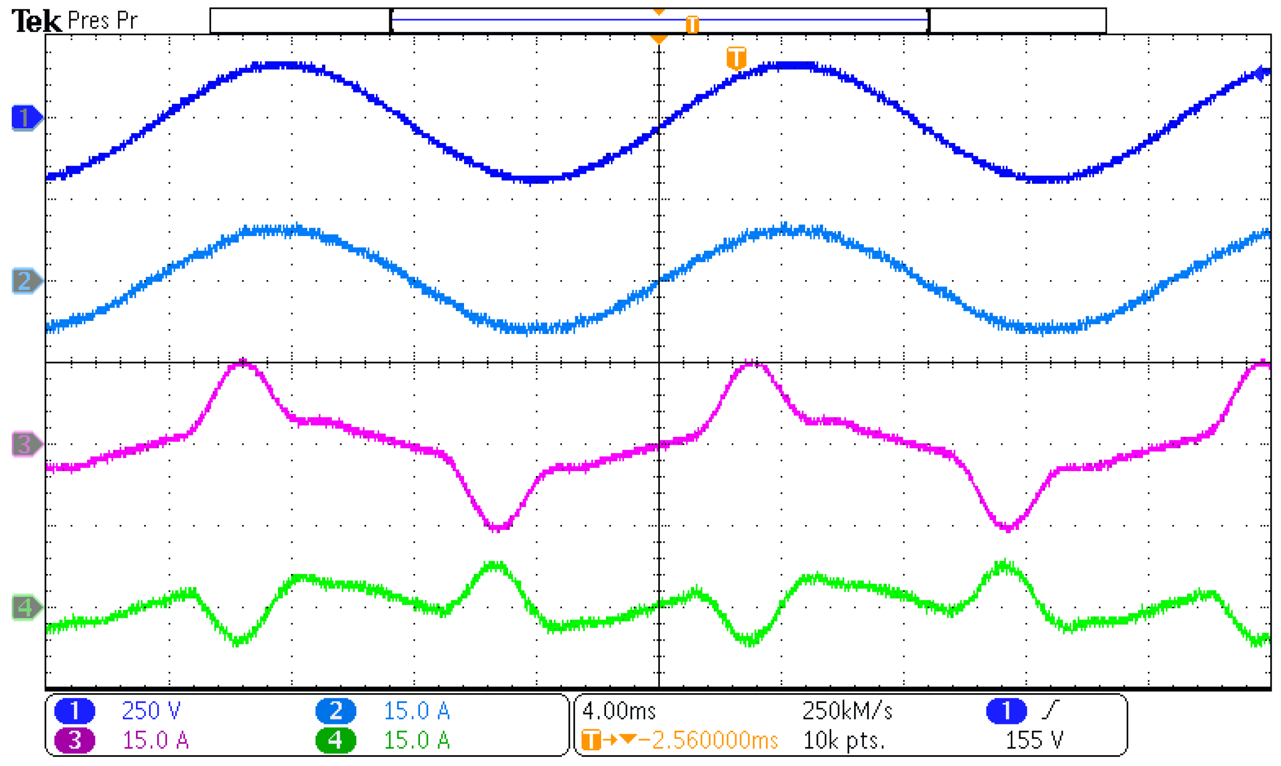
Figure 11 shows the steady state responses (measured at the PCC) of the voltage v PCC , the grid current i G , the current consumed by the NLL i NLL , and the injected current i A F from the SAPF. Notice that the voltage at the PCC presented harmonic distortion. Nevertheless, the grid current i G showed an almost pure sinusoidal waveform in phase with the voltage waveform despite the NLL connected to the PCC. This came from the fact that the fundamental component of v PCC was used as a basis to construct the current reference. This corroborated the tracking of the grid current i G towards its sinusoidal reference.
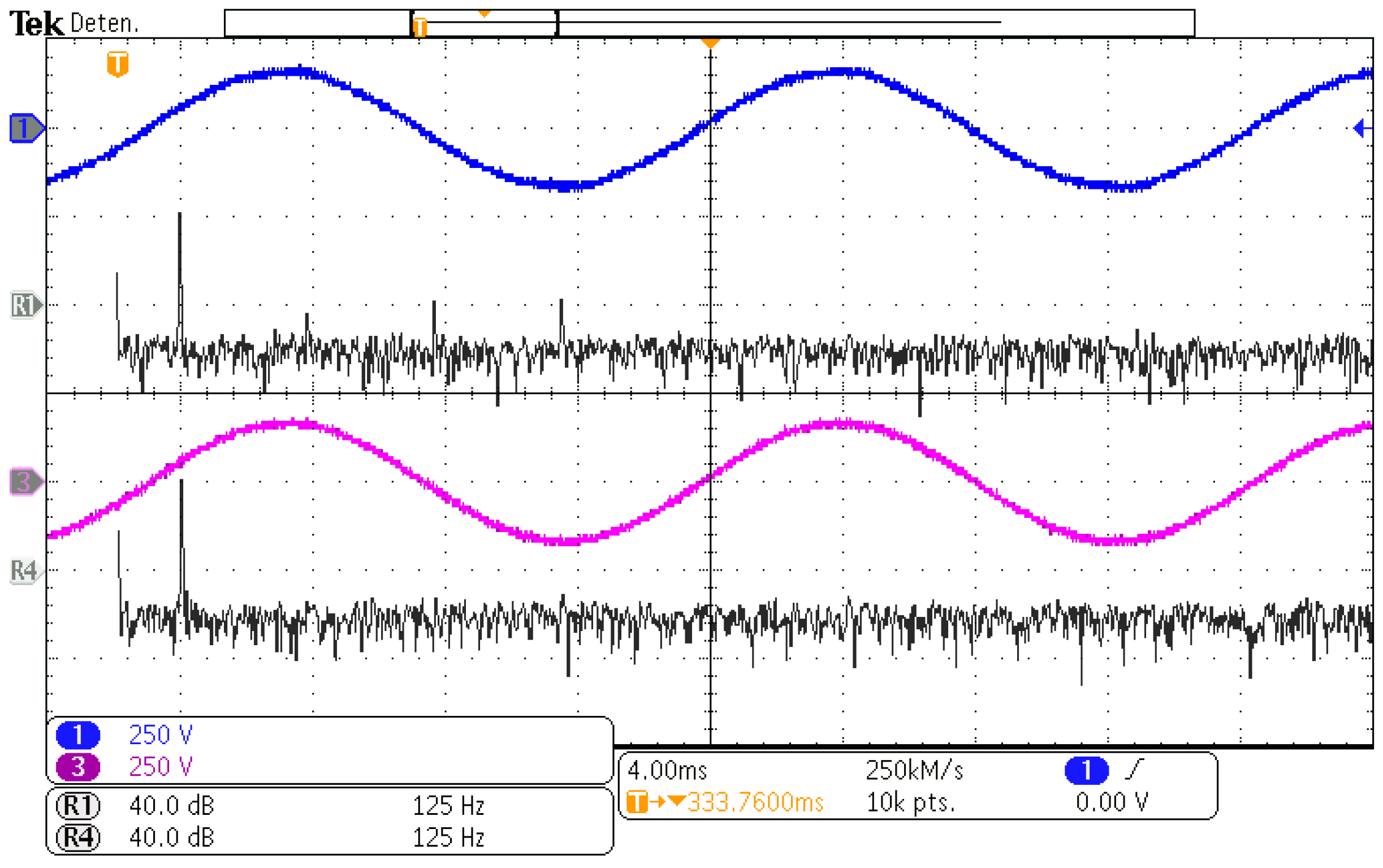
The steady state responses at the PCC of the voltage v PCC and the estimation of its fundamental component v PCC , 1 together with their corresponding frequency spectra are depicted in Figure 12. Notice that the signal v PCC contained harmonic distortion, that is some odd harmonics components were present. Nevertheless, the fundamental component estimate v PCC , 1 did not show any harmonic distortion. This was crucial in the proposed controller as v PCC , 1 was used in the construction of the current reference according to (12).
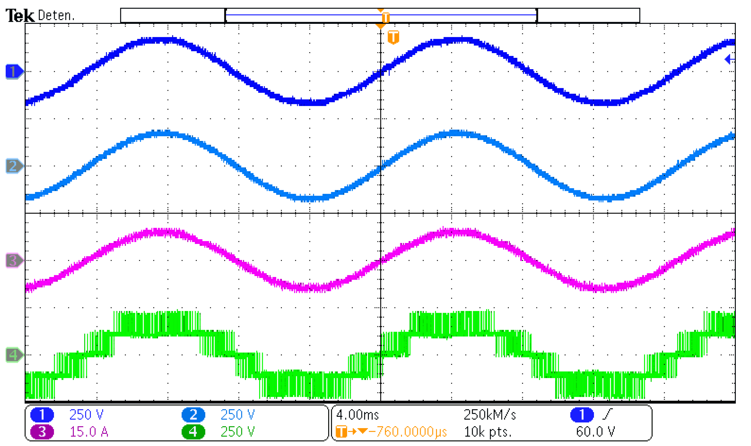
Figure 13 shows the steady state responses of the grid voltage v PCC , the fundamental component estimate of the grid voltage v PCC , 1 , the grid current i G , and the multilevel output voltage generated by the VSI e A F . It can be observed that all signals were in phase, in particular the grid current i G and the voltage v PCC . Furthermore, it can be observed that the injected voltage e A F exhibited five levels, as expected.
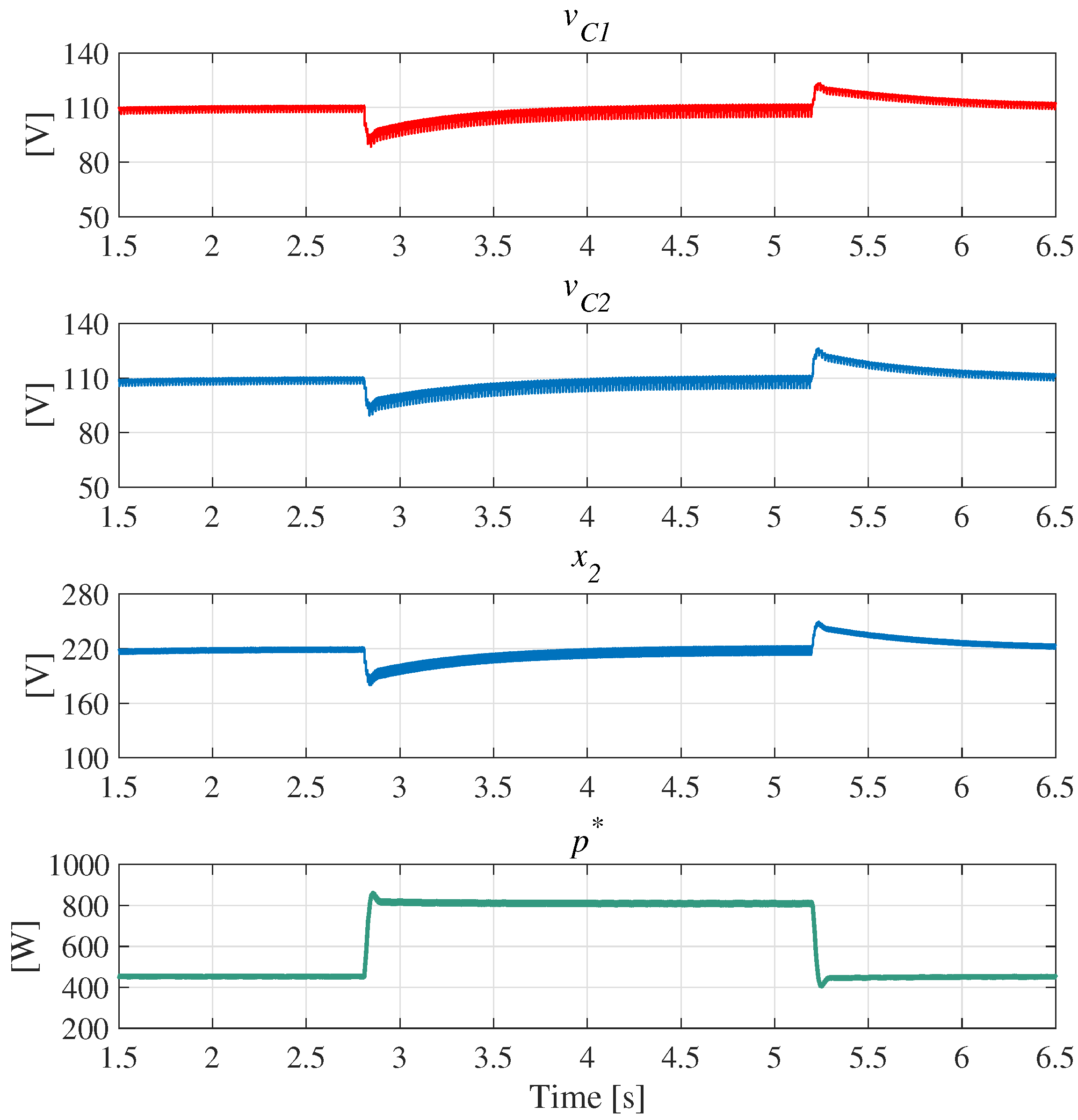
Figure 14 shows the transient responses of v C 1 , v C 2 , x 2 , and p * after i NLL stepwise changes. Notice that the voltage on capacitors v C 1 and v C 2 was maintained at the desired reference after a short transient produced by the step changes in the power demanded by the NLL. This corroborated the effectiveness of the voltage regulation loop.
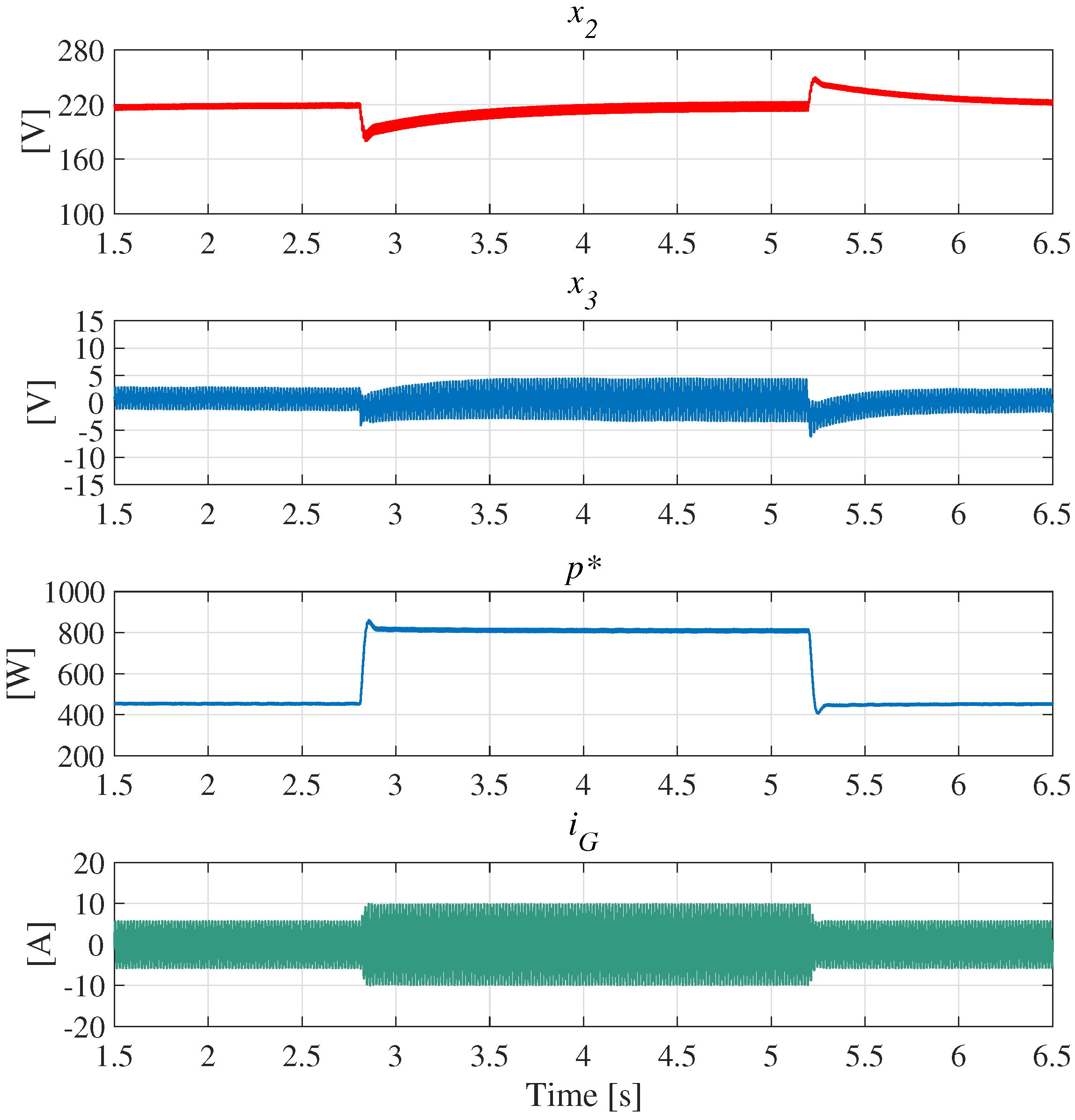
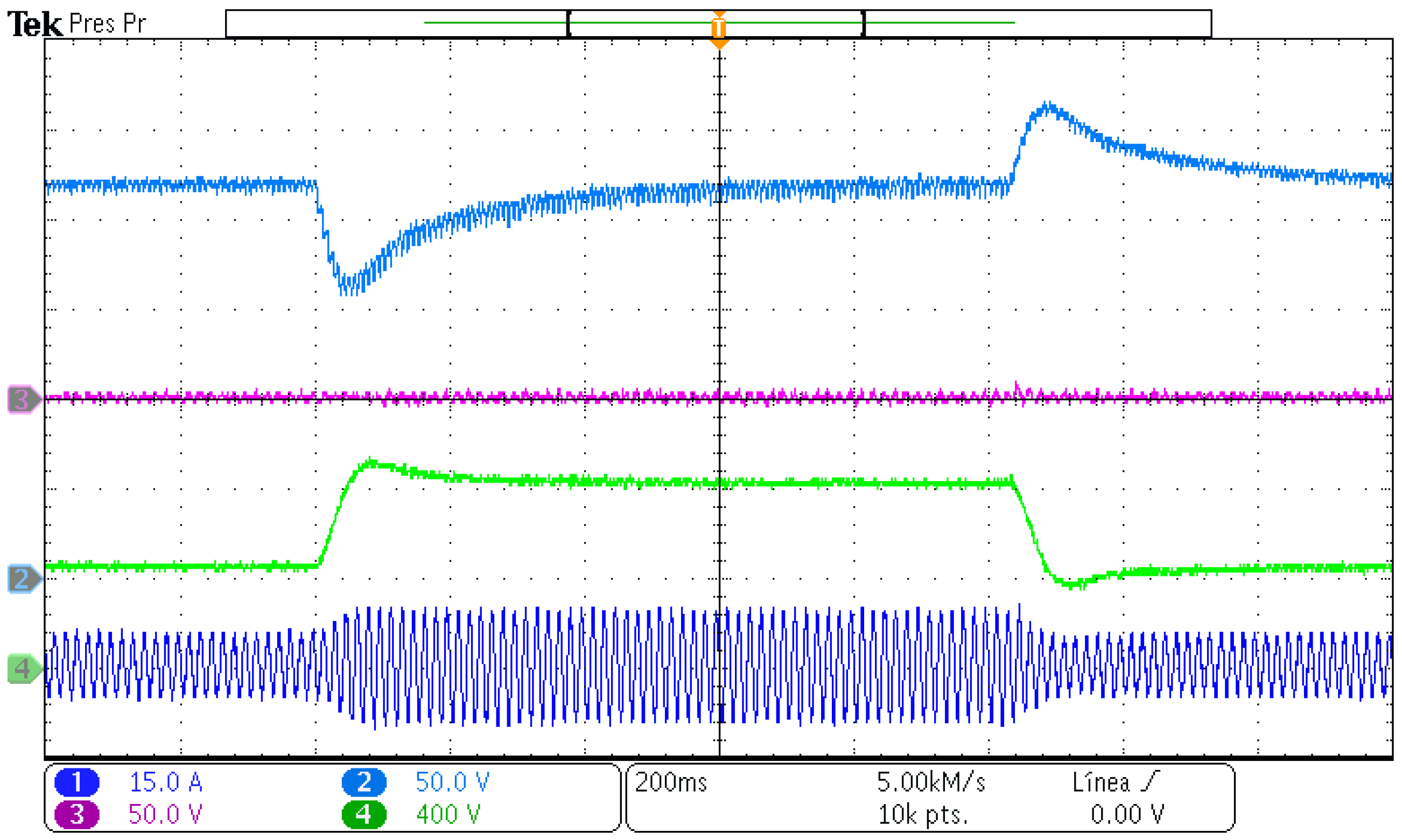
To evaluate the current and voltage dynamical response of the system variables, Figure 15 shows transient responses under the proposed controller during stepwise changes on the power demand p . Notice that the sum of the capacitor voltages x R was regulated to the desired value despite the changes in the power demand. Moreover, it was observed that the capacitor voltage difference, represented by x B , was maintained at zero (in average) and exhibited almost imperceptible transients. This corroborated that the controller guaranteed the voltage balance while keeping the capacitor voltages at a reference of 220 V DC . Note also that the grid current i G increased proportional to the power demanded by the system, and the envelope did not exhibit any overshoot during the transients.
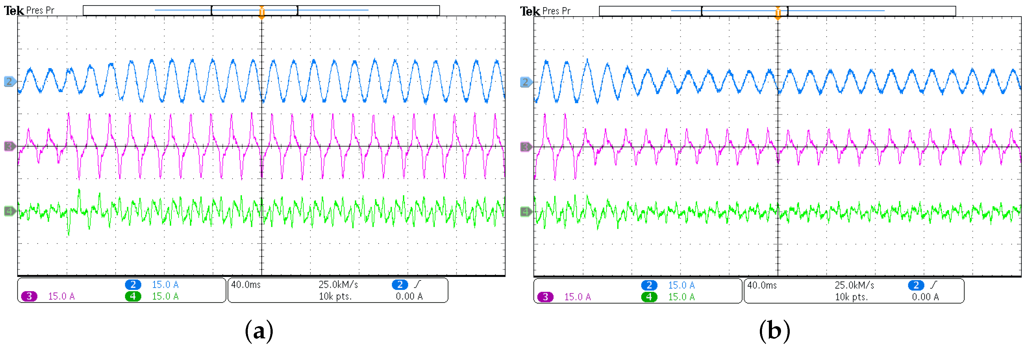
Figure 16 shows the transient responses, during a change of the power demanded by the NLL, of the grid current i G , the current consumed by the NLL i NLL , and the current injected by the SAPF i A F . Notice that, during the stepwise changes on the power demand, the current i G exhibited a fast and smooth response without any overshoot.
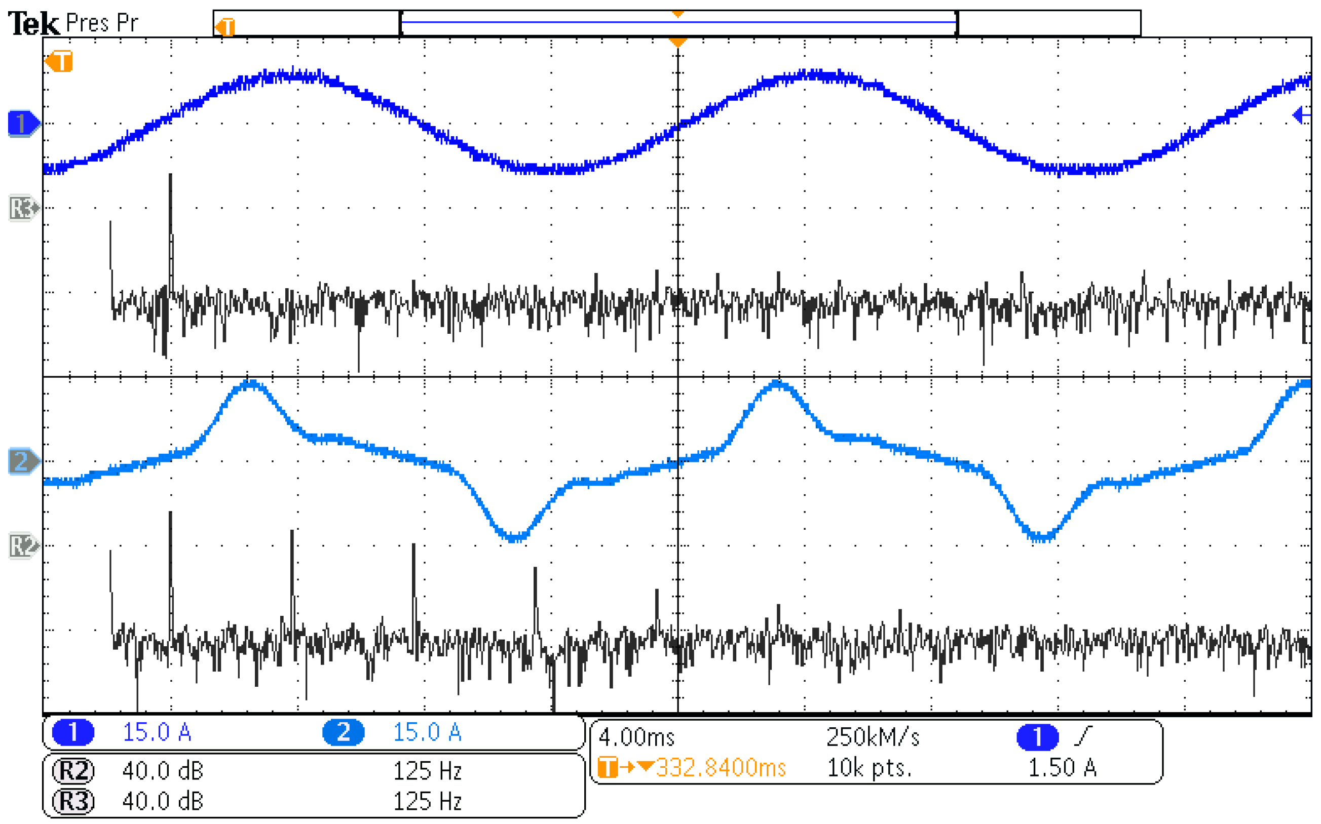
Figure 17 depicts the steady-state responses of the grid current i G and the current consumed by the NLL i NLL , together with their corresponding frequency spectra. Notice that the grid current i G had a quasi-sinusoidal waveform with a THD of 2.32%, while the demanded current by the NLL i NLL had a THD of 53.8%. This represented a noticeable power quality improvement. This was also corroborated by comparing the frequency spectra. Notice that, despite the harmonic pollution observed in the frequency spectra of i NLL , the grid current i G did not exhibit a perceivable harmonic distortion.

5. Concluding Remarks

In this work, a control law for a shunt active power filter based on the five-level full-bridge NPC multilevel topology was presented. The control law comprised three control loops aimed to guarantee the control objectives of grid current tracking, DC-link voltage balance, and DC-link voltage regulation. The resulting control law was designed appealing to a dynamics decoupling assumption. This assumption simplified enormously the control design as it was split into three independent control loops referred to as current, balance, and regulation loops. The current control loop resulted in a combination of a proportional controller aimed to provide damping to the system and a bank of resonant filters aimed to compensate reactive power and harmonic distortion. Regarding the balance and regulation control loops, PI controllers were obtained in each case. In particular, the PI controller of the regulation control loop involved a slight modification, which consisted of the introduction of a low pass filter in the proportional gain to limit the bandwidth of the overall loop. This consideration alleviated the effects and propagation of the unavoidable second harmonics fluctuation in the DC-link voltage produced by the rectification process. Finally, the control law was evaluated in an experimental 2 kW setup of the shunt active power filter based on the five-level full-bridge NPC multilevel topology. The experimental results showed that the active power filter under the proposed controller was able to guarantee an operation with a power factor close to unity and a grid current with less than 5% THD.

Author Contributions

All authors contributed to the development of the overall document, control design, and experimental results. All authors read and agreed to the published version of the manuscript.

Funding

This research was partially supported by Instituto Tecnologico y de Estudios Superiores de Monterrey, Mexico. Also by the PRODEP project “Control de convertidores con alta razon de conversion para aplicacion en energias renovables” (SEP-Mexico) and the UASLP-FAI projects C19-FAI-05-55.55 and C19-FAI-05-45.45.

Conflicts of Interest

The authors declare no conflict of interest.

Abbreviations

The following abbreviations and symbols are used in this manuscript:
5L-HB-NPCFive-level H-bridge neutral point clamped
NLLNonlinear loads
SAPFShunt active power filter
PFPower factor
VSIVoltage source inverter
PCCPoint of common coupling
THDTotal harmonic distortion
PLLPhase locked loop
RMSRoot mean square
v G Grid voltage
ω Grid fundamental frequency
L G Grid inductance
R G Grid resistance
v PPC Voltage at point of common coupling
i G = x G ,Grid current
L F Filter inductance
R F Parasitic filter resistance
C 1 = C 2 = C DC-link capacitors
S 1 ,..., S 8 Converter switches
i A F Filter current
i NLL Nonlinear load current
e A F VSI output voltage
v C 1 , v C 2 Capacitors’ C 1 and C 2 voltages, respectively
δ 1 , δ 2 Switching functions
d 1 , d 2 Duty ratios
x R = v C 1 + v C 2 Voltage regulation state variable
x B = v C 1 v C 2 Voltage balance state variable
u a , u b Control signals
RCapacitors’ discharge resistance
x G * Grid current reference
p Active power reference
v PPC , RMS RMS voltage of v PPC
v PPC , 1 Fundamental component of v PPC
V DC Desired constant value for the DC-link
x R 0 ( t ) Average value of x R
TFundamental period of averaging function
f G Fundamental frequency of grid voltage
V P , h , I N L , h Vectors of unknown harmonic coefficients.
Ψ h Fourier trigonometric vector
x ˜ G Grid current error variable
ϵ A F Vanishing part of e A F
R P = R G + R F Parasitic resistance
ϕ H Sum of periodic signals
k C Proportional gain
ϕ ^ H Harmonic compensation term
ϕ ˜ H Harmonic compensation error
λ h Gain of the h-th oscillator
P L Demanded load power
k p B , k i B Proportional and integral gains of the balance loop.
χ B Balance loop integral variable
z R , z ˜ R Transformation variable and error variable
k i R , k p R Integral and proportional gains of regulation loop
τ R Low-pass filter time constant
ζ R , χ ˙ R Regulation loop integral variable and low-pass filter state
ω B W x G Bandwidth of the closed-loop current subsystem
ω n B , χ Natural oscillation frequency and damping factor of the balance loop
ω n R , ς Natural oscillation frequency and damping factor of the regulation loop
ω B W x R Bandwidth of the closed-loop voltage regulation subsystem

References

  1. Luo, A.; Xu, Q.; Ma, F.; Chen, Y. Overview of power quality analysis and control technology for the smart grid. J. Mod. Power Syst. Clean Energy 2016, 4, 1–9. [Google Scholar] [CrossRef] [Green Version]
  2. Hoon, Y.; Radzi, M.A.M.; Hassan, M.K.; Mailah, N.F. Operation of Three-level Inverter-based Shunt Active Power Filter under Non-ideal Grid Voltage Conditions with Dual Fundamental Component Extraction. IEEE Trans. Power Electron. 2017, 33, 7558–7570. [Google Scholar] [CrossRef]
  3. Guzman, R.; de Vicuña, L.G.; Morales, J.; Castilla, M.; Miret, J. Model-based control for a three-phase shunt active power filter. IEEE Trans. Ind. Electron. 2016, 63, 3998–4007. [Google Scholar] [CrossRef]
  4. Tareen, W.U.K.; Mekhielf, S. Three-Phase Transformerless Shunt Active Power Filter With Reduced Switch Count for Harmonic Compensation in Grid-Connected Applications. IEEE Trans. Power Electron. 2018, 33, 4868–4881. [Google Scholar] [CrossRef]
  5. Martinez-Garcia, J.F.; Martinez-Rodriguez, P.R.; Escobar, G.; Vazquez-Guzman, G.; Sosa-Zuñiga, J.M.; Valdez-Fernandez, A.A. Effects of modulation techniques on leakage ground currents in a grid-tied transformerless HB-NPC inverter. IET Renew. Power Gener. 2019, 13, 1250–1260. [Google Scholar] [CrossRef]
  6. Rodriguez, J.; Bernet, S.; Steimer, P.; Lizama, I. A Survey on Neutral-Point-Clamped Inverters. IEEE Trans. Ind. Electron. 2010, 57, 2219–2230. [Google Scholar] [CrossRef]
  7. Akagi, H.; Isozaki, K. A Hybrid Active Filter for a Three-Phase 12-Pulse Diode Rectifier Used as the Front End of a Medium-Voltage Motor Drive. IEEE Trans. Power Electron. 2012, 27, 69–77. [Google Scholar] [CrossRef]
  8. Feng, L.; Wang, Y. Modeling and Resonance Control of Modular Three-Level Shunt Active Power Filter. IEEE Trans. Ind. Electron. 2017, 64, 7478–7486. [Google Scholar] [CrossRef]
  9. Angulo, M.; Ruiz-Caballero, D.A.; Lago, J.; Heldwein, M.L.; Mussa, S.A. Active power filter control strategy with implicit closed-loop current control and resonant controller. IEEE Trans. Ind. Electron. 2013, 60, 2721–2730. [Google Scholar] [CrossRef]
  10. Antoniewicz, K.; Jasinski, M.; Kazmierkowski, M.P.; Malinowski, M. Model predictive control for three-level four-leg flying capacitor converter operating as shunt active power filter. IEEE Trans. Ind. Electron. 2016, 63, 5255–5262. [Google Scholar]
  11. Salim, C. Five-level (NPC) shunt active power filter performances evaluation using fuzzy control scheme for harmonic currents compensation. In Proceedings of the 2017 6th International Conference on Systems and Control (ICSC), Batna, Algeria, 7–9 May 2017; pp. 561–566. [Google Scholar]
  12. Morsli, A.; Tlemçani, A.; Cherchali, N.O.; Boucherit, M.S. Comparison between PI and fuzzy logic type-1 controllers for improvement the power quality by a shunt active power filter five-level NPC topology. In Proceedings of the 2016 8th International Conference on Modelling, Identification and Control (ICMIC), Algiers, Algeria, 15–17 November 2016; pp. 243–248. [Google Scholar]
  13. Bonala, A.K.; Sandepudi, S.R.; Muddineni, V.P. Improved model predictive current control for single-phase NPC shunt active power filter. In Proceedings of the 2016 IEEE International Conference on Power Electronics, Drives and Energy Systems (PEDES), Kerala, India, 14–17 December 2016; pp. 1–6. [Google Scholar]
  14. Acuna, P.; Morán, L.; Rivera, M.; Aguilera, R.; Burgos, R.; Agelidis, V.G. A single-objective predictive control method for a multivariable single-phase three-level NPC converter-based active power filter. IEEE Trans. Ind. Electron. 2015, 62, 4598–4607. [Google Scholar] [CrossRef]
  15. Munoz, J.; Espinoza, J.; Baier, C.; Moran, L.; Guzman, J.; Cardenas, V. Decoupled and Modular Harmonic Compensation for Multilevel STATCOMs. IEEE Trans. Ind. Electron. 2014, 61, 2743–2753. [Google Scholar] [CrossRef]
  16. Rodriguez, J.; Lai, J.S.; Peng, F.Z. Multilevel inverters: A survey of topologies, controls, and applications. IEEE Trans. Ind. Electron. 2002, 49, 724–738. [Google Scholar] [CrossRef] [Green Version]
  17. Kim, S.H.; Kim, Y.H.; Seo, K.M.; Bang, S.S.; Kim, K.S. Harmonic analysis and output filter design of NPC multi-level inverters. In Proceedings of the 2006 37th IEEE Power Electronics Specialists Conference, Jeju, Korea, 18–22 June 2006; pp. 1–5. [Google Scholar] [CrossRef]
  18. Nasiri, M.R.; Farhangi, S.; Rodríguez, J. Model Predictive Control of a Multilevel CHB STATCOM in Wind Farm Application Using Diophantine Equations. IEEE Trans. Ind. Electron. 2019, 66, 1213–1223. [Google Scholar] [CrossRef]
  19. Dash, A.R.; Panda, A.K.; Patel, R.; Penthia, T. Design and implementation of a cascaded transformer coupled multilevel inverter-based shunt active filter under different grid voltage conditions. Int. Trans. Electr. Energy Syst. 2019, 29, 01–20. [Google Scholar] [CrossRef]
  20. Franquelo, L.G.; Rodriguez, J.; Leon, J.I.; Kouro, S.; Portillo, R.; Prats, M.A.M. The age of multilevel converters arrives. IEEE Ind. Electron. Mag. 2008, 2, 28–39. [Google Scholar] [CrossRef] [Green Version]
  21. Kouro, S.; Malinowski, M.; Gopakumar, K.; Pou, J.; Franquelo, L.G.; Wu, B.; Rodriguez, J.; Pérez, M.A.; Leon, J.I. Recent Advances and Industrial Applications of Multilevel Converters. IEEE Trans. Ind. Electron. 2010, 57, 2553–2580. [Google Scholar] [CrossRef]
  22. Kumar, R.; Bansal, H.O. Real-time implementation of adaptive PV-integrated SAPF to enhance power quality. Int. Trans. Electr. Energy Syst. 2019, 29, 01–22. [Google Scholar] [CrossRef]
  23. Radzi, M.A.M.; Rahim, N.A. Neural network and bandless hysteresis approach to control switched capacitor active power filter for reduction of harmonics. IEEE Trans. Ind. Electron. 2009, 56, 1477–1484. [Google Scholar] [CrossRef]
  24. Rodriguez, J.; Cortes, P. Predicitive Control of Power Converters and Electrical Drives; John Wiley & Sons, Ltd.: Hoboken, NJ, USA, 2012. [Google Scholar]
  25. Luo, A.; Xu, X.; Fang, L.; Fang, H.; Wu, J.; Wu, C. Feedback-feedforward PI-type iterative learning control strategy for hybrid active power filter with injection circuit. IEEE Trans. Ind. Electron. 2010, 57, 3767–3779. [Google Scholar] [CrossRef]
  26. Mu, X.; Wang, J.; Wu, W.; Blaabjerg, F. A Modified Multifrequency Passivity-Based Control for Shunt Active Power Filter With Model-Parameter-Adaptive Capability. IEEE Trans. Ind. Electron. 2018, 65, 760–769. [Google Scholar] [CrossRef]
  27. Sertac, B.; Hasan, K. A Sliding-Mode Controlled Single-Phase Grid-Connected Quasi-Z-Source NPC Inverter With Double-Line Frequency Ripple Suppression. IEEE Access 2019, 7, 160004–160016. [Google Scholar] [CrossRef]
  28. Martinez-Rodriguez, P.R.; Escobar-Valderrama, G.; Sosa-Zuniga, J.M.; Vazquez-Guzman, G.; Mendoza-Mendoza, J.d.J. Analysis and experimental validation of a controller for a single-phase active power filter based on a 3L-NPC topology. Int. Trans. Electr. Energy Syst. 2017, 27, e2385. [Google Scholar] [CrossRef]
  29. Barrena, J.; Marroyo, L.; Vidal, M.; Apraiz, J. Individual Voltage Balancing Strategy for PWM Cascaded H-Bridge Converter-Based STATCOM. IEEE Trans. Ind. Electron. 2008, 55, 21–29. [Google Scholar] [CrossRef]
  30. Bosch, S.; Staiger, J.; Steinhart, H. Predictive Current Control for an Active Power Filter With LCL-Filter. IEEE Trans. Ind. Electron. 2018, 65, 4943–4952. [Google Scholar] [CrossRef]
  31. Tarisciotti, L.; Formentini, A.; Gaeta, A.; Degano, M.; Zanchetta, P.; Rabbeni, R.; Pucci, M. Model Predictive Control for Shunt Active Filters with Fixed Switching Frequency. IEEE Trans. Ind. Appl. 2017, 53, 296–304. [Google Scholar] [CrossRef]
  32. Escobar, G.; Leyva-Ramos, J.; Carrasco, J.M.; Galvan, E.; Portillo, R.C.; Prats, M.M.; Franquelo, L.G. Modeling of a three level converter used in a synchronous rectifier application. In Proceedings of the 2004 IEEE 35th Annual Power Electronics Specialists Conference (IEEE Cat. No.04CH37551), Aachen, Germany, 20–25 June 2004; pp. 4306–4311. [Google Scholar] [CrossRef]
  33. Alepuz, S.; Busquets-Monge, S.; Bordonau, J.; Gago, J.; Gonzalez, D.; Balcells, J. Interfacing Renewable Energy Sources to the Utility Grid Using a Three-Level Inverter. IEEE Trans. Ind. Appl. 2006, 53, 1504–1511. [Google Scholar] [CrossRef]
  34. Valdez-Fernandez, A.; Martinez-Rodriguez, P.; Escobar, G.; Limones-Pozos, C.; Sosa, J. A Model-Based Controller for the Cascade H-Bridge Multilevel Converter Used as a Shunt Active Filter. IEEE Trans. Ind. Electron. 2013, 60, 5019–5028. [Google Scholar] [CrossRef]
  35. Escobar, G.; Martinez-Rodriguez, P.R.; Ho, C.N.M.; Sosa, J.M. Design of an inverter-side current reference and controller for a single-phase LCL-based grid-connected inverter. Int. Trans. Electr. Energy Syst. 2018, 28, e2476. [Google Scholar] [CrossRef]
  36. Khalil, H.K. Nonlinear Systems; Prentice Hall: Hoboken, NJ, USA, 2002. [Google Scholar]
  37. Francis, B.; Wonham, W. The internal Model Principle for Linear Multivariable Regulators. Appl. Math. Optim. 1975, 2, 170–194. [Google Scholar] [CrossRef]
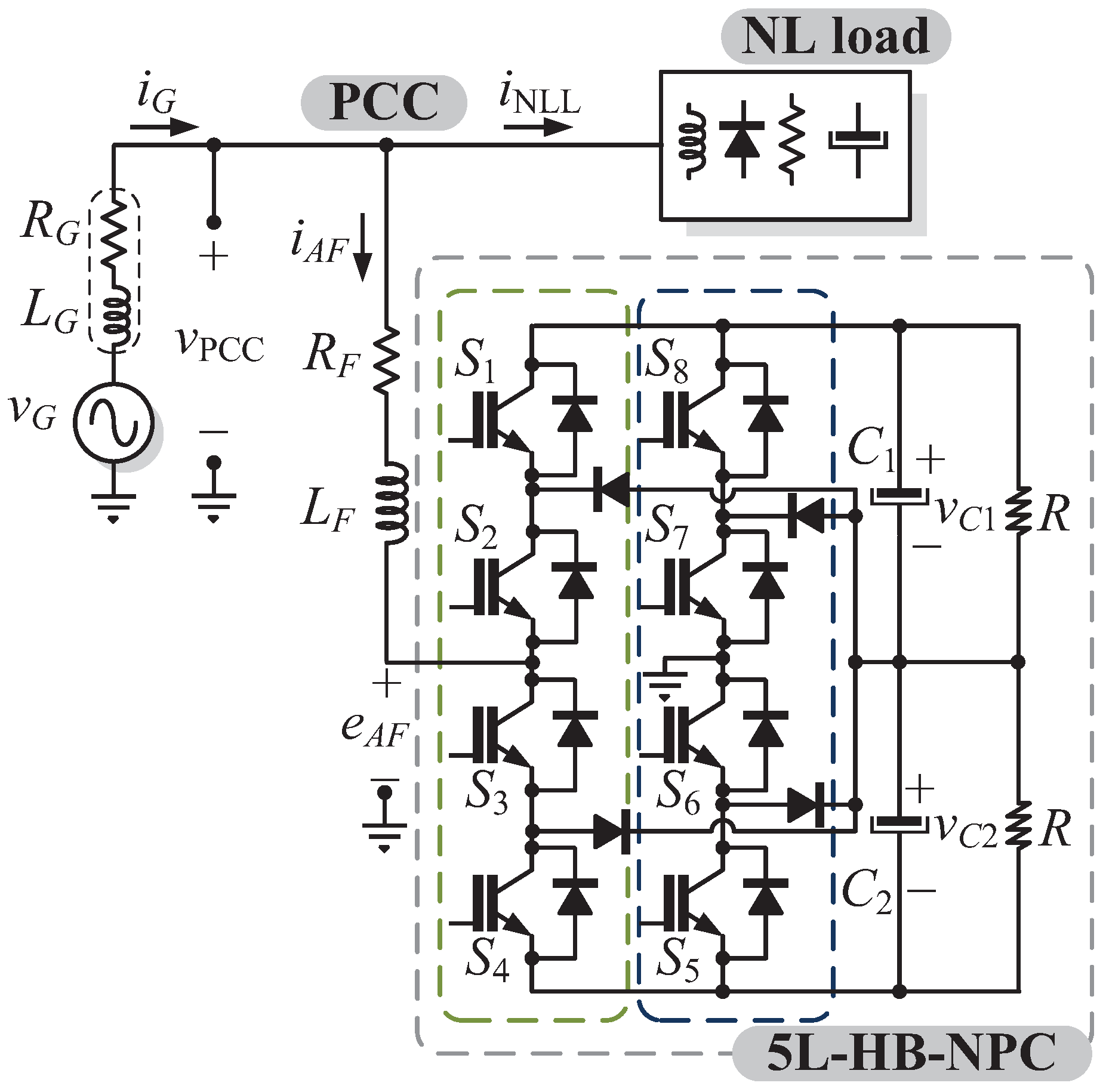
Figure 1. Single-phase SAPF based on a 5L-HB-NPC topology.
Energies 13 01691 g001
Figure 2. Equivalent diagram of the SAPF based on the 5L-HB-NPC topology with the switching functions δ 1 and δ 2 .
Energies 13 01691 g002
Figure 3. Block diagram of the proposed controller.
Energies 13 01691 g003
Figure 4. Experimental setup of the 5L-HB-NPC as the SAPF.
Energies 13 01691 g004
Figure 5. Steady state responses of the voltage at the PCC v PCC , the line current i G , the current consumed by the NLL i NLL , and the injected current i A F .
Energies 13 01691 g005
Figure 6. Steady state responses of the grid voltage v PCC , the fundamental component of the grid voltage v PCC , 1 , the line current i G , and the multilevel output voltage of the inverter e A F .
Energies 13 01691 g006
Figure 7. Transient responses of the voltage across each capacitor of the DC-Link v C 1 , v C 2 , the sum of the capacitors voltage x 2 , and the power reference calculated in the regulation loop p * during a load change.
Energies 13 01691 g007
Figure 8. Transient responses of the sum of the capacitors voltages x 2 , the difference of the capacitors voltages x 3 , the power reference p * , and the line current i G during a load change.
Energies 13 01691 g008
Figure 9. Transient responses of the line current i G , the current consumed by the NLL i NLL , and the current injected by the SAPF i A P F , during a change of the power demanded by the NLL: (a) from low to high load and (b) from high to low load.
Energies 13 01691 g009
Figure 10. Steady state responses of the voltage at the PCC v PCC , the compensated line current i G , the current consumed by the NLL i NLL with RLload, and the injected current i A F with the inductive output filter of (a) L F = 3 mH and (b) L F = 1 mH.
Energies 13 01691 g010
Figure 11. Steady state responses at the PCC after the current compensation process of: (CH1) the voltage v PCC (y-axis 250 V/div); (CH2) the grid current i G (y-axis 15 A/div); (CH3) the current consumed by the NLL i NLL (y-axis 15 A/div); and the injected current i A F (y-axis 15 A/div, x-axis 4 ms/div).
Energies 13 01691 g011
Figure 12. Steady state responses at the PCC of: (CH1) the voltage v PCC (y-axis 250 V/div, x-axis 4 ms/div); (R1) the frequency spectra of v PCC (y-axis 40 dB/div, x-axis 125 Hz/div); (CH3) the fundamental component estimate of the grid voltage v PCC , 1 (y-axis 250 V/div, x-axis 4 ms/div); and (R4) the frequency spectra of v PCC , 1 (y-axis 40 dB/div, x-axis 125 Hz/div).
Energies 13 01691 g012
Figure 13. Steady state responses of: (CH1) the grid voltage v PCC (y-axis 250V/div); (CH2) the fundamental component estimate of the grid voltage v PCC , 1 (y-axis 250V/div); (CH3) the line current i G (y-axis 15 A/div); and (CH4) the multilevel output voltage generated by the VSI e A F (y-axis 250 V/div).
Energies 13 01691 g013
Figure 14. Transient responses during NLL stepwise changes of: (CH1) the capacitor voltage v C 1 (y-axis 50 V/div); (CH2) the capacitor voltage v C 2 (y-axis 50 V/div); (CH3) the sum of the capacitors voltages x 2 (y-axis 50 V/div); and (CH4) the power reference p * calculated in the regulation loop (y-axis 400 W/div).
Energies 13 01691 g014
Figure 15. Transient responses during NLL stepwise changes of: (CH1) the sum of the capacitor voltage x 2 (y-axis 50 V/div); (CH2) the difference of the capacitors voltages x 3 (y-axis 50 V/div); (CH3) the power reference p * calculated in the regulation loop (y-axis 50 V/div); and (CH4) the grid current i G .
Energies 13 01691 g015
Figure 16. Transient responses, during a change in the power demanded by the NLL, of: (CH2) the grid current i G ; (CH3) the current consumed by the NLL i NLL ; and (CH4) the current injected by the SAPF i A F : (a) from low to high load and (b) from high to low load (y-axis 15 A/div, x-axis 40 ms/div in all cases).
Energies 13 01691 g016
Figure 17. Steady state responses of: (CH1) the grid current i G (y-axis 15 A/div, x-axis 4 ms/div); (R2) the frequency spectra of i G (y-axis 40 dB/div, x-axis 125 Hz/div); (CH2) the current consumed by the NLL i NLL (y-axis 15 A/div, x-axis 4 ms/div); and (R3) the frequency spectra of i NLL (y-axis 40 dB/div, x-axis 125 Hz/div).
Energies 13 01691 g017
Table 1. Switching states of the 5L-HB-NPC.
State δ 1 δ 2 S 1 S 2 S 3 S 4 S 5 S 6 S 7 S 8 e AF ( V )
11−111001100 v C 1 + v C 2
21011000110 + v C 1
30−101101100 + v C 2
400001111000
500011001100
600110000110
70101100011 v C 1
8−1000110110 v C 2
9−1100110011 ( v C 1 + v C 2 )
Table 2. System parameters.
SAPF NLL-L NLL-H
ParameterValueParameterValueParameterValue
v PCC 127 V RMS at 60 Hz R N L 1 85 Ω R N L 2 100 Ω
L F 3 mH C N L 1 45 μ F C N L 2 45 μ F
C 1 = C 2 1880 μ F R L 1 75 Ω R L 2 100 Ω
f s w 7 kHz L L 1 8 mH L L 2 7 mH
R40 k Ω
R s t 100 Ω
Table 3. Controller parameters.
Tracking LoopRegulation LoopBalance Loop
k C = 20 k i R = 0.016 k i B = 0.0008
λ 1 = 300 k p R = 0.035 k p B = 0.01
λ 3 = 700 τ R = 60
λ 5 = 1450 V DC = 220
λ 7 = 800
λ 9 = 80
λ 11 = 60
λ 13 = 60