Abstract
This research proposes a four-level T-type inverter that is suitable for low-power applications. The presented topology outranks other types of inverters in terms of a smaller number of semiconductor devices, absence of passive components such as clamping diodes and flying capacitors, low switching and conduction losses, and high efficiency. The proposed topology is free from voltage deviation and unbalanced voltage occurrences that are present in other multilevel converters having clamping diodes or flying capacitors. The proposed inverter can extend to N levels using unequal dc-link voltage sources for medium-voltage application. The inverter employs the simple fundamental frequency staircase modulation technique. Moreover, this paper presents a current commutation strategy to prevent the occurrences of short circuit and minimizing the number of required switching devices and switching transitions, resulting in improving the efficiency of the inverter. This paper also analyses the theoretical converter losses showing lower switching and conduction losses when compared to existing four-level inverters. The experimental validation of the proposed inverter shows its operating feasibility and a low output voltage THD.
1. Introduction
Multilevel inverters have been developed widely in industrial applications in recent decades [1]. The conventional topologies employed for industrial applications are neutral point clamped (NPC), flying capacitor (FC), and cascaded H-bridge (CHB) inverters [2,3,4]. However, with higher output voltage levels, the conventional multilevel inverters pose disadvantages such as unbalanced dc-link voltage, practical limits to the number of output voltage level, and high component count [5].
Recently, numerous research has been proposed on asymmetrical and hybrid multilevel inverters, which have different values of dc voltage sources and dc-link circuits that are connected to the midpoint such as the inverter presented in [6]. Various modulation techniques [7,8,9,10] and power electronic component technologies [11,12,13,14] are needed to achieve the desired output stepped waveforms. Various types of switches have been constructed and validated in [15,16] for different types of inverters for the purpose of increasing the reliability of the inverters such as to reduce the total count of passive components and to obtain the desired stepped output waveforms [17,18,19].
Industrial applications constantly require multilevel inverters with high rated power and high-power quality. However, the two requirements cannot be achieved while maintaining low switching frequency [20]. The T-type inverter can be an alternative for low-voltage applications, meeting the requirements of high-power quality at a lower switching frequency [1]. In addition, T-type topology has the advantage of two-level converters, which include low power losses, simple operation, and the positive aspects of the three-level converters, such as higher efficiency and smoother stepped output voltage waveforms [21].
T-type inverters are mainly proposed and constructed for low-power industrial applications since it shows a better performance compared to the conventional inverters [22,23,24,25,26,27]. Although T-type inverters consist of two switches in series connection in its T-link, the efficiency is higher, and the power losses are lower compared to the conventional inverters. In other words, T-type inverters are also good solutions for low-voltage applications with high power ratings obtained by increasing the phase current [28].
For medium- and high-voltage applications, a bidirectional switch is applied to the midpoint of the T-type inverter and can be an alternative solution to minimize the number of components [29,30,31,32,33]. T-type inverters that are applied for medium-voltage and medium-power applications are known as neutral point piloted (NPP) [34,35] and the transistor-clamped converter (TCC) [36]. Medium-voltage applications are achieved by connecting additional semiconductor switches in series in the main inverter bridge. However, gate-drive control units are required to balance the turn-off voltage of each series-connected switch and smooth transient during the operations [37,38]. Moreover, the series connection increases conduction and switching losses.
This paper proposes a four-level T-type inverter (4LT2C) that generates 0, 1Vdc, 2Vdc, and 3Vdc voltage levels without any capacitors and clamping devices. The presented topology outranks other topologies in terms of efficiency, low output voltage total harmonic distortion, and a low number of switching devices. For the embedded solar system, the 4LT2C can be placed with two isolated batteries for four-level output voltages, which is much less costly than the installation of a bypass filter in a landing application. In addition, the 4LT2C are extendable to N levels by adding auxiliary dc-link circuits that consist of a dc-link source and two semiconductor switches. This work aims to minimize the switching transitions and increase the efficiency of the 4LT2C and extended inverters by decreasing the component count of power components, and conduction and switching losses. In this paper, Section 2 describes the proposed topology, its structure, modulation technique and switching sequences. Section 3 presents the operating principles of the 4LT2C and its extended structure. Section 4 explains the simulation results, presents the efficiency analysis and comparison with other multilevel topologies. The theoretical analysis of the proposed topology shows good performance when compared to other four-level NPC, FC, and CHB in terms of the number of components, simplicity, and high efficiency. Section 5 shows the experimental setup and results of the 4LT2C.
2. The Proposed 4LT2C Converter
2.1. The Proposed Converter Topology and Model
Figure 1 shows the proposed 4LT2C consisting of the conventional two-level VSC with active bidirectional switches at the T-link, and multilevel dc-link with unequal voltage sources. In the proposed 4LT2C, the upper switches (Q1, Q3 and Q5) of the three legs are connected to the positive part of the voltage supply, whereas the lower switches (Q2, Q4 and Q6), which operate complementarily with the upper switches, are connected to ground (g). Furthermore, the dc-link with unequal dc voltage sources are connected to the midpoint of the main bridge via two series active bidirectional switches in each leg a, b, and c. The proposed 4LT2C differs from the four-level topology illustrated in [2] because the 4LT2C has reduced dc-link sources and switches for the same output level, resulting in the reduction of cost and complexity. An increased number of output voltage steps reduces output total harmonic distortion (THD), while a decreased number of semiconductor switches minimizes conduction and switching losses. The 4LT2C three-phase line-to-ground voltages are expressed as [28],
where N is the number of voltage levels and in the proposed inverter, and Sa, Sb, and Sc are the voltage factors at the midpoint of legs a, b, and c, respectively. Moreover, the reference line-to-ground voltages are found as,
where Ma is set to 1 and ωt is the electrical angle. The line-to-neutral voltages are written as,
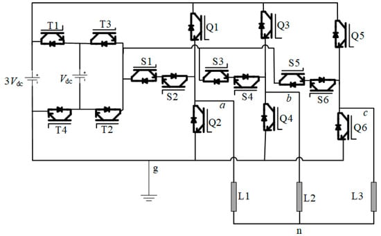
Figure 1.
Schematic of the proposed four-level T-type converter (4LT2C) where each single-bridge leg of the T-type VSC resembles the shape of the rotated character “T”.
2.2. Modulation Technique and Operating Principle
The modulation strategy is a very important feature in designing converters with high efficiency. In the proposed inverter, either the staircase modulation technique [2] or the pulse width modulation technique can be applied successfully.
Table 1 illustrates the four possible switching states of leg a and the corresponding line-to-ground voltage Vag when staircase modulation is employed. Based on the switching sequence shown in Table 1, the line-to-ground voltages in leg a of 3Vdc is obtained when the upper switch Q1 turns on and zero is obtained when the lower switch Q2 turns on. Both Q1 and Q2 cannot turn on at the same time to prevent the shoot-through event. Moreover, with the dc-link combination, each leg can produce +2Vdc and +1Vdc, successively. Note that Table 1 has not considered the method to reduce the number of switching transitions. Table 1 shows that the bidirectional switches in the T-link leg a (S1 and S2) have the same switching state in each cycle. During the transition between voltage levels, the current flow is no longer based on the current direction [4].

Table 1.
Voltage transition and switching states in leg a.
Table 2 presents the switching states of Q1–Q6 in the main bridge, T1–T4 in the dc-link and S1-S6 in the T-link. The corresponding voltage sequence in legs a, b, and c, are also shown in the table, where 3, 2, 1, and 0 are related to the dc-link voltage. The highlighted parts in Table 2 shows the switching transitions of the dc-link switches in which T1 and T2 are operated in contrast with T3 and T4. Moreover, Table 2 shows the condition of switches S1 and S2, which are turned on to reduce the switching losses during the transition from 3Vdc to 2Vdc. When switch Q1 is turned on, leg a will generate 3Vdc, and it will not be affected by the state of switches S1 and S2 being turned on. This is due to the current passing through Q1, a low resistance path, as compared to the higher resistance dc-link path via S1 and S2. By controlling S1 and S2 in the on state when Q1 is turned on, the number of turn-on and turn-off transitions are reduced because S1 and S2 are required to be turned on when Sa is 1 or 2. This also effectively increases the efficiency of the inverter. Figure 2 presents the space vector modulation switching states with a modulation index of 1 that can be used as a switching strategy in the proposed 4LT2C. All the parameters of the voltage vector are calculated according to the value of the d and q components [2]. The dq components of the space vector references can be obtained from the following equations [28]
where Sa, Sb, and Sc are the dc voltage factor at the midpoint of legs a, b, and c. Note that the dc-link switches of the proposed 4LT2C function produce 1Vdc or 2Vdc at the output of one of the legs in the main inverter at any one time. Therefore, the voltage sequences of 122, 123, or 221 cannot be achieved with the space vector modulation of the modulation index less than 1. In other words, the synchronization of generating 1Vdc or 2Vdc cannot happen since switches T1 and T2 are operating in complementary with switches T3 and T4.
Table 2.
Voltage transition and switching states over 1 cycle with reduced switching transitions.
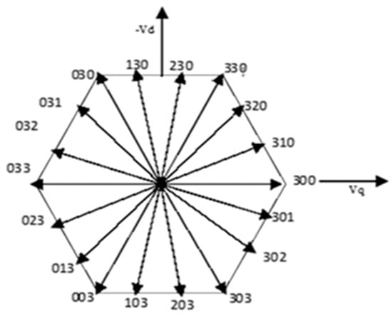
Figure 2.
Switching state vectors for 4LT2C [28].
2.3. The Proposed Commutation Strategy and Extended Structure
The inverter is suitable to be operated with staircase modulation, a type of fundamental frequency modulation technique, and PWM and SVM that are high-frequency modulation techniques. However, this paper proposes a commutation strategy in Section 4 that minimizes the number of switching transitions in the 4LT2C when operated in the staircase modulation technique. The efficiency analysis in Section 5 will show that the efficiency of the proposed inverter is increased due to the enhanced staircase modulation.
The switching commutation that requires adequate consideration is elaborated in detail in this section. The current commutation strategy which operates separately from the current direction is taken into account to prevent any short circuit in the dc-link and active bidirectional switches. Furthermore, the switching states of each leg and its line-to-ground voltage are modified to apply a simple turn-on delay and current commutation strategy for all switches.
Table 3 shows the new switching states of leg a and the line-to-ground voltage Vag after the switch commutation is considered. As shown in Table 3, applying the current commutation strategy contributes to decreasing the switching times of the dc-link switches, in which case the switching and conduction losses are minimized. Additionally, implementing this strategy enhances the performance of the proposed 4LT2C by increasing its efficiency and reducing power losses [6].
Table 3.
Voltage transition and modified switching state in leg a.
The modified switching state demonstrates that in implementing the current commutation strategy, Q1 and S1 must be closed to achieve 3Vdc. At the same time, Q2 and S2 should be closed to obtain a zero-voltage level. In a multilevel inverter, a short circuit in any leg can occur during a transition between the voltage levels. The duration of the required time between the on state and off state of the switches in a multilevel inverter is the time that the short circuit current occurrence can take place. Therefore, in the proposed topology, the current commutation strategy is applied in order to make the right path for continuous current flow.
Figure 3 presents the current commutation strategy for the transition from 3Vdc to 2Vdc, which effectively enhances the switching time of 4LT2C to prevent the occurrence of short circuits inside the dc-link circuit. Figure 3a illustrates the positive current commutation during the switching transition of 3Vdc to the 2Vdc. The midpoint of leg a is connected to dc-link source 3Vdc when Q1 and S1 are turned on. To obtain the voltage of 2Vdc, T1 and T2 are set in an on state. During the commutation from 3Vdc to 2Vdc, switch Q1 must be turned off first. After the turn-on delay, S2 is also turned on. As shown in Figure 3b, between the turning off Q1 and the turning on S2, the current reverses direction via T1, DT2, S1, and DS2 so that the voltage level at the midpoint of leg a becomes 2Vdc, while S2 turns on in the zero-voltage condition. However, the negative output current still passes through DQ1 when Q1 is turned off.
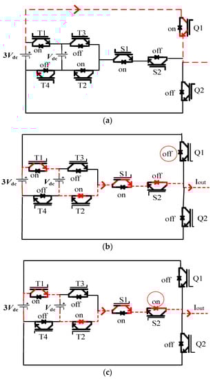
Figure 3.
Current commutation during switching transition of positive output current in leg a. (a) Output voltage level of 3Vdc (Q1 on and S2 off). (b) Output voltage level of 2Vdc (Q1 off and DS2 on). (c) Output voltage level of 2Vdc (Q1 off, DS2 on and S2 on with ZVS).
Figure 4 shows that the two switches of T3 and T4 in the dc-link are turned on to provide Vdc to the bidirectional switches of leg a during a negative phase output current. A positive phase output current naturally commutates to DQ2 when S1 is turned off. However, a negative phase output current continues to pass through S2, DS1, DT3, and T4 during the turning off of S1. After a delay time, Q2 is turned on and the current commutates to Q2. Figure 5 presents the various extended dc-link for the T-type topology.
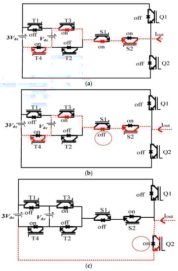
Figure 4.
Current commutation during switching transition of negative output current in leg a. (a) Output voltage level of Vdc (Q2 off and DS1 on). (b) Output voltage level of Vdc (Q2 off and S1 off on ZVS). (c) Output voltage level of 0 (Q2 on and S1 off).
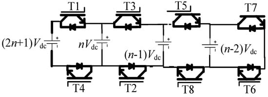
Figure 5.
Extended structure of the dc-link of the proposed 4LT2C.
Figure 5 shows that the level of dc-link sources in the proposed 4LT2C can be simply extended to increase the number of output voltage levels. The maximum dc voltage is (2n + 1)Vdc. When , the 4LT2C consisting of T1–T4 and dc sources of 3Vdc and Vdc is achieved. When the dc-link is extended to the number of additional dc-link switches are T5 and T8 and the dc sources are 5Vdc, 2Vdc, and Vdc.
3. Simulation Results and Analysis
3.1. Operating Waveforms of the Proposed 4LT2C
Figure 6 depicts the gate switching signals and the idealized line-to-neutral and line-to-line staircase waveforms of the proposed 4LT2C. The levels of line-to-line voltage are +3Vdc, +2Vdc, 1Vdc, 0, −1Vdc, −2Vdc, and −3Vdc.
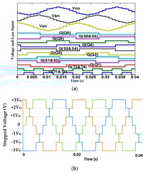
Figure 6.
Idealized waveforms. (a) Gate signals and the line-to-neutral voltages Vcn, Vbn, and Van. (b) Waveforms for the line-to-line voltages Vab, Vbc, and Vca.
Figure 7 depicts the simulation results for the proposed four-level inverter. Note that Vdc is equal to 100 V in the simulation. The four-step waveforms of the line-to-line and line-to-ground voltages, and five-step waveforms of the line-to-neutral voltage shown are as per the idealized waveforms of the proposed 4LT2C. Each level of the line-to-line voltage is equal to Vdc. The output waveform of the load current is generated in accordance with the output stepped voltages. Therefore, the proposed inverter is validated successfully via simulation.
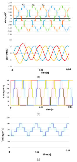
Figure 7.
Simulation results for 4LT2C (a) line-to-neutral voltages & load current, (b) line-to-ground voltages (c), and neutral to ground voltage.
3.2. Voltage Transition and Switching Energy Loss of the Proposed 4LT2C and the N-Level Inverter in
Figure 8 shows one leg of the N-level inverter in [2] and the proposed 4LT2C that are used in the switching loss analysis. Table 4 and V illustrate the voltage transition and switching energy loss of components in leg a of the proposed 4LT2C and the N-level inverter in [2] during positive and negative output currents, respectively. In addition, Table 4 and subcircuits shown in Figure 3 and Figure 4 explain in detail the process of the current commutation and switching transitions of the proposed 4LT2C topology. The analysis of the switching transition in Table 4 indicates that the number of devices in 4LT2C that turn on and off during the voltage transitions is two-thirds of the switching transitions shown in Table 5 for the N-level inverter [2]. Thus, the conduction and switching losses significantly decline during the current commutation and voltage transition process. In this case, the total efficiency of the inverter is enhanced accordingly.
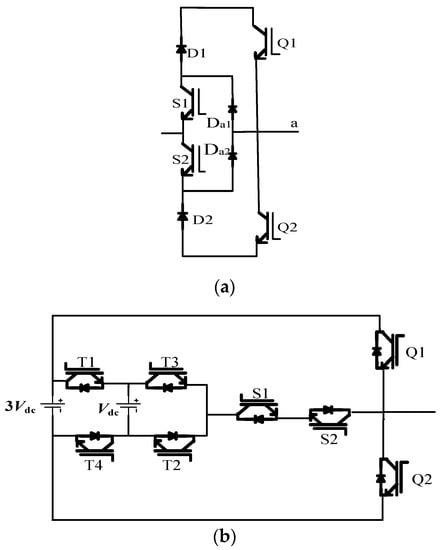
Figure 8.
One leg of (a) the N-level inverter in [2] and (b) the 4LT2C.
Table 4.
Switching energy loss of the phase a components in the proposed 4LT2C.
Table 5.
Switching energy loss of the phase a components in the N-level inverter proposed in [2].
3.3. Efficiency Analysis of the Proposed 4LT2C and the N-Level Inverter in [2]
The efficiency analysis is carried out by assuming that the proposed converter is connected to a three-phase 20 Ω-7 mH RL load. The IGBTs selected are rated at 19 A and 600 V (Model No. -HGTG20N60B3D). Using the information provided in the datasheet and the curve-fitting tool in MATLAB [1], the function of collector–emitter voltage is,
where i(t) is the instantaneous load current. Moreover, the on-state and off-state energy losses and are
and
In order to estimate the efficiency of the proposed 4LT2C, the conduction and switching losses energy are calculated in different values of output power. This inverter is designed to deliver the rated power of Pout = 2.25 kW with dc-link voltages of Vdc = 100 V and 3Vdc = 300 V. The switching loss Psw is calculated as,
where is the diode reverse recovery energy dissipation.
The switching losses are calculated by analyzing the voltage transition process from a higher level to a lower level as shown in Table 4 and Table 5. The N-level inverter in [2] has a higher number of IGBT and diode switching energy losses than the 4LT2C. The total switching loss is the summation of the switching energy loss of IGBT and diodes over one reference period.
The IGBT and diode conduction losses, and are calculated [28] as,
and
The conduction losses based on the conducting time, the structure of the inverter and value of the load current. Additionally, Table 6 shows the conducting devices of 4LT2C for phase a.
Table 6.
Conducting devices of the 4LT2C for phase a.
The total losses in the 4LT2C and N-level inverter are,
The efficiency of the converter is calculated as the ratio of the output and input power as,
Figure 9 compares the switching and conduction losses and the efficiency of the proposed 4LT2C and the N-level inverter base on [2] by applying the same operating conditions. Figure 8a,b shows that in the proposed converter, the switching and conduction losses per leg are 35.635 W and 0.6972 W, respectively. The switching and conduction losses per leg in the N-level inverter in [2] are 41.757 W and 1.1152 W, respectively. Figure 9c indicates that the 4LT2C reaches the maximum efficiency of 95.38%, while the N-level inverter presented in [2] reaches the maximum efficiency of 94.60% at the rated power of 2.25 kW. The proposed converter operates with high efficiency and lower power losses compared to N-level inverter in [2] because of the reduced number of IGBTs and minimized number of switching times during a commutation.
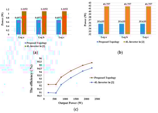
Figure 9.
Comparison of calculated losses and efficiency between 4LT2C and the four-level inverter in [2]: for Ma = 1 and Pout = 2.250 kW. (a) Switching losses in each leg. (b) Conduction losses in each leg. (c) Efficiency as the output power increases to 2.25 kW.
3.4. Comparison of Component and Ratings of the Proposed 4LT2C with Other Multilevel Topologies
Figure 10 presents the topology for the nested multilevel configuration with four-level inverter in [40], four-level inverter proposed in [41] and a typical diode clamped multilevel inverter. Table 7 compares the proposed 4LT2C with the recent four-level inverter from [39,40], the four-level inverter proposed in [2], and the other existing topology shown in Figure 9, in terms of the number of switches, diodes, capacitors and dc sources. It can be clearly seen that the component count in the 4LT2C is lower than the other converters. Therefore, the 4LT2C will perform better than the N-level inverter in [2] and the other three multilevel inverters in terms of reduced switching and conduction losses and lower cost. Additionally, the topology presented in [39,40] consists of 18 switches and six flying capacitors. Therefore, the proposed 4LT2C is more advantageous in terms of fewer conduction losses.
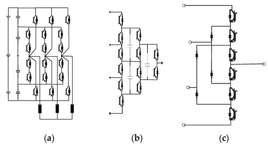
Figure 10.
Topologies proposed in the technical literature. (a) Nested multilevel configuration with four levels [41]. (b) Four-level inverter proposed by [4]. (c) Diode clamping multilevel inverter.
Table 7.
Comparison between the proposed 4LT2C and other topologies.
Moreover, the absence of flying capacitors in the proposed topology signifies the avoidance of any unbalanced voltage that may occur between the capacitors during the operation of the inverter.
4. The 4LT2C Prototype and Experimental Results
Figure 11 presents the experimental setup to verify the proposed 4LT2C. The setup consists of gate drivers, a dSPACE CP1104, a personal computer to run the switching algorithm developed in MATLAB/Simulink, two isolated dc voltage supplies set at 90 V and 30 V each, 16 IGBT switches (HGT20N60B3D, 19 A, 600 V), heat sinks, and an induction motor (400 V, 0.81 A, 0.3 kW, 50 Hz, 2800 min−1). In addition, device voltage rating in the proposed T-type inverter of N levels is shown in Table 8. The proposed converter is operated using the staircase modulation technique with a fundamental frequency f = 50 Hz.

Figure 11.
A prototype of the proposed 4LT2C.
Table 8.
N-level T-Type inverter component rating.
Figure 12 illustrates the results of the experiment on the proposed 4LT2C. The results above indicate that the outcomes of the experiments are the same as the simulation results shown in Figure 3. Furthermore, Figure 11c shows that the output voltage total harmonic distortion without any filter is 11.836% in the proposed topology. The frequency spectrum presents the occurrence of odd harmonics.
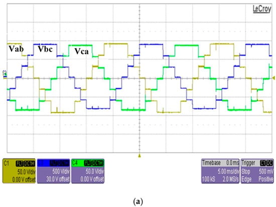
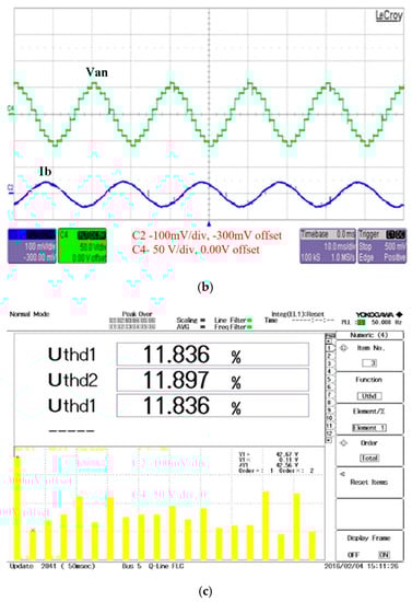
Figure 12.
The experimental results for 4LT2C when connected to 0.3 kW induction motor load. (a) Line-to-line voltage. (b) Line-to-neutral voltage with load current. (c) The total harmonic distortion (THD) of the proposed topology.
Components that can be removed by applying an appropriate modulation technique. Thus, the 4LT2C is better than the other common inverters, as indicated in the analysis, discussion, and experimental results.
Table 9 presents the comparison of 4LT2C with the existing four-level multilevel converter topology according to the number of components, rating requirement and blocking voltages. It is understood that the T-type inverter is an improved version of the NPC inverter. However, the comparison as mentioned in the previous sections is also included for the sake of completeness. Furthermore, Table 7 shows that 4LT2C has fewer components than the other types of four-level inverters. In other words, 4LT2C has fewer number of switches compared to the other inverters, thereby decreasing the conduction and switching losses of the inverter.
Table 9.
Comparison of neutral point clamped (NPC), cascaded H-bridge (CHB), flying capacitor (FC), and NLT2C in terms of rating requirement per the N level.
The proposed 4LT2C can be used for applications in PV grids and automotive inverter systems [21]. The proposed topology is implemented on induction motor load in the experimental setup. The topology is suitable for low-power applications as it has minimal conduction and switching losses and low component count as compared to the other four-level inverter. The proposed converter can be used for medium-voltage applications. However, a series connection of semiconductor switches in the upper and lower arm of the main inverter may be necessary. Series connection of semiconductor devices comes with problems of unequal switching times and lower reliability. Therefore, the proposed converter is recommended for low-voltage and low-power (<1000 V) applications such as induction motors, photovoltaics, and household appliances.
5. Conclusions
This paper has proposed a three-phase four-level T-type inverter (4LT2C) that can be easily extended to N levels by adding the desired number of dc supplies to the variable dc-link. The analysis of the switching operation in the 4LT2C using staircase modulation technique with proposed commutation strategy has shown that the inverter has a low number of switching transitions and hence exhibits lower conduction and switching losses in comparison with other common four-level topologies. The experimental results have verified the operating feasibility of the proposed converter and commutation strategy. A low output voltage THD without any filter is also achieved, resulting in a sinusoidal current with induction motor load. The proposed 4LT2C has advantages in term of a low component count, low conduction and switching losses, and simplicity of the structure for higher-level output voltage as compared to other types of four-level inverter topologies. Moreover, the presented topology consists of no passive components such as clamping diodes and flying capacitors, which results in no issues of voltage deviation and unbalanced output voltages in the 4LT2C. Since the proposed converter has a lower switching and conduction loss, and minimized component count, the 4LT2C is recommended for high-efficiency and low-voltage applications at a low cost. In addition, the proposed topology can be implemented in the nanogrid models using different types of PV panels connected to control current DC/DC converter or in hybrid energy storage systems using two isolated batteries. The 4LT2C can also be used for medium-voltage applications. However, the series connection of semiconductor switches in the upper and lower arms of the main inverter in the topology may be needed.
Author Contributions
S.S.A. has contributed to the theoretical approaches, simulation, experimental tests, and preparing the article; S.M. has contributed to the theoretical approaches, simulations, experimental tests, and preparing the article; H.M. has contributed to the theoretical approaches and preparing the article. N.M.L.T. has contributed to the theoretical approaches and preparing the article. All authors have read and agreed to the published version of the manuscript.
Funding
This work presented herein was supported in parts by University of Malaya under Large Research Grant Scheme (LRGS): LR008-2019 and Universiti Tenaga Nasional BOLD2025 Grant under Project Code 10436494/B/2019133. The APC was supported by UNITEN BOLD Publication Fund.
Conflicts of Interest
The authors declare no conflicts of interest.
Abbreviations
| 4LT2C | Four-level T-type converter |
| D1~D6, Da1~Dc2, Dz1~Dz4 | Inverter diodes |
| VSC | Voltage source converter |
| Eon | Turn-on losses |
| Eoff | Turn-off losses |
| Vce | The block-voltage or reverse-voltage |
| Pcond_IGBT | Power conduction losses of the IGBT |
| Pcond_diode | Power conduction losses of the diode |
| Psw | The power switching losses |
| fsw | The operation switching frequency of switch |
| g | The inverter ground |
| Q1~Q6 | Switches of the main bridge |
| T1~T4 | Switches of DC-link |
| G(Q1)~G(Q6) | Switching gate signals |
| G(T1)~G(T4) | |
| G(S1)~G(S6) | |
| Ia, Ib, Ic, Iab | Load currents |
| Ma | Amplitude of the modulation index |
| N | Number of output voltage levels |
| Sa, Sb, Sc | Inverter switching states |
| Vdc | Voltage step value |
| Vref | Reference voltage vector |
| Vd | d-voltage component |
| Vq | q-voltage component |
| Vp | Voltage peak amplitude |
| Vag, Vbg, Vcg | Line-to-ground output voltages |
| Van, Vbn, Vcn | Inverter line-to-neutral voltages |
| Von_IGBT | Forward voltage drops in IGBT |
| Von_diode | Forward voltage drops in Diode |
References
- Kouro, S.; Malinowski, M.; Gopakumar, K.; Pou, J.; Franquelo, L.G.; Wu, B.; Rodriguez, J.; Pérez, M.A.; Leon, J.I. Recent advances and industrial applications of multilevel converters. IEEE Trans. Ind. Electron. 2010, 57, 2553–2580. [Google Scholar] [CrossRef]
- Masaoud, A.; Ping, H.W.; Mekhilef, S.; Taallah, A.; Belkamel, H. Design and Implementation of a new multilevel DC-Link three-phase inverter. J. Power Electron. 2014, 14, 292–301. [Google Scholar] [CrossRef]
- Glauber de Almeida Cacau, R.; Torrico-Bascope, R.P.; Aberides Ferreira Neto, J.; Torrico-Bascope, G.V. Five-Level T-Type Inverter Based on Multistate Switching Cell. IEEE Trans. Ind. Appl. 2014, 50, 3857–3866. [Google Scholar] [CrossRef]
- Dos Santos, E.C.; Muniz, J.H.; da Silva, E.R.; Jacobina, C.B. Nested multilevel topologies. IEEE Trans. Power Electron. 2015, 30, 4058–4068. [Google Scholar] [CrossRef]
- Peng, F.Z.; Qian, W.; Cao, D. Recent advances in multilevel converter/inverter topologies and applications. In Proceedings of the 2010 International Power Electronics Conference (IPEC), Sapporo, Japan, 21–24 June 2010. [Google Scholar]
- Masaoud, A.; Ping, H.W.; Mekhilef, S.; Taallah, A.S. New three-phase multilevel inverter with reduced number of power electronic components. IEEE Trans. Power Electron. 2014, 29, 6018–6029. [Google Scholar] [CrossRef]
- Belkamel, H.; Mekhilef, S.; Masaoud, A.; Naeim, M.A. Novel three-phase asymmetrical cascaded multilevel voltage source inverter. IET Power Electron. 2013, 6, 1696–1706. [Google Scholar] [CrossRef]
- Mekhilef, S.; Kadir, M.N.A. Voltage control of three-stage hybrid multilevel inverter using vector transformation. IEEE Trans. Power Electron. 2010, 25, 2599–2606. [Google Scholar] [CrossRef]
- Mei, J.; Xiao, B.; Shen, K.; Tolbert, L.M.; Zheng, J.Y. Modular multilevel inverter with new modulation method and its application to photovoltaic grid-connected generator. IEEE Trans. Power Electron. 2013, 28, 5063–5073. [Google Scholar] [CrossRef]
- Mariethoz, S. Systematic design of high-performance hybrid cascaded multilevel inverters with active voltage balance and minimum switching losses. IEEE Trans. Power Electron. 2013, 28, 3100–3113. [Google Scholar] [CrossRef]
- Babaei, E. A cascade multilevel converter topology with reduced number of switches. IEEE Trans. Power Electron. 2008, 23, 2657–2664. [Google Scholar] [CrossRef]
- Nami, A.; Zare, F.; Ghosh, A.; Blaabjerg, F. A hybrid cascade converter topology with series-connected symmetrical and asymmetrical diode-clamped H-bridge cells. IEEE Trans. Power Electron. 2011, 26, 51–65. [Google Scholar] [CrossRef]
- Mathew, J.; Mathew, K.; Azeez, N.A.; Rajeevan, P.P.; Gopakumar, K. A Hybrid Multilevel Inverter System Based on Dodecagonal Space Vectors for Medium Voltage IM Drives. IEEE Trans. Power Electron. 2013, 28, 3723–3732. [Google Scholar] [CrossRef]
- Saeedifard, M.; Barbosa, P.M.; Steimer, P.K. Operation and control of a hybrid seven-level converter. IEEE Trans. Power Electron. 2012, 27, 652–660. [Google Scholar] [CrossRef]
- Park, S.-J.; Kang, F.-S.; Lee, M.H.; Kim, C.-U. A new single-phase five-level PWM inverter employing a deadbeat control scheme. IEEE Trans. Power Electron. 2003, 18, 831–843. [Google Scholar] [CrossRef]
- Klumpner, C.; Blaabjerg, F. Using reverse-blocking IGBTs in power converters for adjustable-speed drives. IEEE Trans. Ind. Appl. 2006, 42, 807–816. [Google Scholar] [CrossRef]
- Ping, H.W.; Rahim, N.A.; Jamaludin, J. New three-phase multilevel inverter with shared power switches. J. Power Electron. 2013, 13, 787–797. [Google Scholar] [CrossRef]
- Bohari, A.A.; Goh, H.H.; Tonni, A.K.; Lee, S.S.; Sim, S.Y.; Goh, K.C.; Lim, C.S.; Luo, Y.C. Predictive Direct Power Control for Dual-Active-Bridge Multilevel Inverter Based on Conservative Power Theory. Energies 2020, 13, 2951. [Google Scholar] [CrossRef]
- Rawa, M.; Siddique, M.D.; Mekhilef, S.; Mohamed Shah, N.; Bassi, H.; Seyedmahmoudian, M.; Horan, B.; Stojcevski, A. Design and implementation of a hybrid single T-type double H-bridge multilevel inverter (STDH-MLI) topology. Energies 2019, 12, 1810. [Google Scholar] [CrossRef]
- Abu-Rub, H.; Holtz, J.; Rodriguez, J.; Baoming, G. Medium-voltage multilevel converters—State of the art, challenges, and requirements in industrial applications. IEEE Trans. Ind. Electron. 2010, 57, 2581–2596. [Google Scholar] [CrossRef]
- Schweizer, M.; Kolar, J.W. Design and implementation of a highly efficient three-level T-type converter for low-voltage applications. IEEE Trans. Power Electron. 2013, 28, 899–907. [Google Scholar] [CrossRef]
- Holtz, J. Selbstgeführte Wechselrichter mit treppenförmiger Ausgangsspannung für grosse Leistung und hohe Frequenz. Siemens Forsch. Entwickl. 1977, 6, 164–171. [Google Scholar]
- Nabae, A.; Takahashi, I.; Akagi, H. A new neutral-point-clamped PWM inverter. IEEE Trans. Ind. Appl. 1981, 518–523. [Google Scholar] [CrossRef]
- Steinke, J. Grundlagen für die Entwicklung eines Steuerverfahrens für GTO-Dreipruktwechselrichter für Traktionsantriebe. ETZ-Archiv 1988, 10, 215–220. [Google Scholar]
- Joetten, R.; Gekeler, M.; Eibel, J. AC drive with three-level voltage source inverter and high dynamic performance microprocessor control. In Proceedings of the European Conference on Power Electronics and Applications, EPE, Brussels, Belguim, 16–18 October 1985. [Google Scholar]
- Fuld, B. Aufwandsarmer Thyristor-Dreistufen-Wechsebrichter mit geringen Verlusten. ETZ-Archiv 1989, 11, 261–265. [Google Scholar]
- Takeshita, T.; Matsui, N. PWM control and input characteristics of three-phase multi-level AC/DC converter. In Proceedings of the PESC’92 Record, 23rd Annual IEEE Power Electronics Specialists Conference, Toledo, Spain, 29 June–3 July 1992. [Google Scholar]
- Shueai Alnamer, S.; Mekhilef, S.; Bin Mokhlis, H.J.E. A Four-Level T-Type Neutral Point Piloted Inverter for Solar Energy Applications. Energies 2018, 11, 1546. [Google Scholar] [CrossRef]
- Brückner, T.; Bernet, S.; Güldner, H. The active NPC converter and its loss-balancing control. IEEE Trans. Ind. Electron. 2005, 52, 855–868. [Google Scholar] [CrossRef]
- Leredde, A.; Gateau, G.; Floricau, D. New three level topology with shared components: Properties, losses, and control strategy. In Proceedings of the 35th Annual Conference of IEEE Industrial Electronics (IECON’09), Porto, Portugal, 3–5 November 2009. [Google Scholar]
- Li, J.; Liu, J.; Boroyevich, D.; Mattavelli, P.; Xue, Y. Three-level active neutral-point-clamped zero-current-transition converter for sustainable energy systems. IEEE Trans. Power Electron. 2011, 26, 3680–3693. [Google Scholar] [CrossRef]
- Ewanchuk, J.; Salmon, J.; Knight, A.M. Performance of a high-speed motor drive system using a novel multilevel inverter topology. IEEE Trans. Ind. Appl. 2009, 45, 1706–1714. [Google Scholar] [CrossRef]
- Xiao, H.; Xie, S. Transformerless split-inductor neutral point clamped three-level PV grid-connected inverter. IEEE Trans. Power Electron. 2012, 27, 1799–1808. [Google Scholar] [CrossRef]
- Peron-Guennegues, V.; Conilh, C.; Leclere, L. A converter topology for high current density drive applications. In Proceedings of the 2011: 14th European Conference on Power Electronics and Applications (EPE 2011), Birmingham, UK, 30 August–1 September 2011. [Google Scholar]
- Umashankar, S.; Reddy, R. NPP Inverter Topology for Renewable Energy Applications. Indian J. Electr. Comput. Eng. 2013, 1, 31–38. [Google Scholar]
- Chen, B.; Yao, W.; Lu, Z. Novel five-level three-phase hybrid-clamped converter with reduced components. J. Power Electron. 2014, 14, 1119–1129. [Google Scholar] [CrossRef][Green Version]
- Baraia, I.; Barrena, J.A.; Abad, G.; Segade, J.M.C.; Iraola, U. An experimentally verified active gate control method for the series connection of IGBT/diodes. IEEE Trans. Power Electron. 2012, 27, 1025–1038. [Google Scholar] [CrossRef]
- Withanage, R.; Shammas, N. Series connection of insulated gate bipolar transistors (IGBTs). IEEE Trans. Power Electron. 2012, 27, 2204–2212. [Google Scholar] [CrossRef]
- Peng, F.Z. A generalized multilevel inverter topology with self voltage balancing. IEEE Trans. Ind. Appl. 2001, 37, 611–618. [Google Scholar] [CrossRef]
- Wu, W.; Wang, D.J.I.A. An optimal voltage-level based model predictive control approach for four-level T-type nested neutral point clamped converter with reduced calculation burden. IEEE Access 2019, 7, 87458–87468. [Google Scholar] [CrossRef]
- Bahrami, A.; Narimani, M. A sinusoidal pulsewidth modulation (SPWM) technique for capacitor voltage balancing of a nested T-type four-level inverter. IEEE Trans. Power Electron. 2018, 34, 1008–1012. [Google Scholar] [CrossRef]
- Kordic, M.; Narimani, M.; Alimardani, M. A New Hybrid Multilevel Nested Neutral Point Clamped (NNPC) Converter. In Proceedings of the 2018 IEEE Canadian Conference on Electrical & Computer Engineering (CCECE), Quebec City, QC, Canada, 13–16 May 2018. [Google Scholar]
© 2020 by the authors. Licensee MDPI, Basel, Switzerland. This article is an open access article distributed under the terms and conditions of the Creative Commons Attribution (CC BY) license (http://creativecommons.org/licenses/by/4.0/).