Article

A Family of Single-Stage, Buck-Boost Inverters for Photovoltaic Applications

1
School of Automation, Northwestern Polytechnical University, Xi’an 710072, China
2
Department of Electrical Engineering, Holon Institute of Technology, Holon 58102, Israel
3
Department of Energy Technology, Aalborg University, 9220 Aalborg, Denmark
*
Author to whom correspondence should be addressed.
Energies 2020, 13(7), 1675; https://doi.org/10.3390/en13071675
Submission received: 5 February 2020 / Revised: 9 March 2020 / Accepted: 21 March 2020 / Published: 3 April 2020

Abstract

:
This paper introduces a family of single-stage buck-boost DC/AC inverters for photovoltaic (PV) applications. The high-gain feature was attained by applying a multi-winding tapped inductor, and thus, the proposed topologies can generate a grid-level AC output voltage without using additional high step-up stages. The proposed topologies had a low component count and consisted of a single magnetic device and three or four power switches. Moreover, the switches were assembled in a push-pull or half/full-bridge arrangement, which allowed using commercial low-cost driver-integrated circuits. In this paper, the operation principle and comparison of the proposed topologies are presented. The feasibility of the proposed topologies was verified by simulations and experimental tests.

1. Introduction

The continuous development of distributed photovoltaic (PV) power generation systems arouses much interest in MIEs/MICs, also known as microinverters. Unlike the string inverters using series-connected PV panels to achieve a high voltage, microinverters are designed to directly connect a single PV panel with a low voltage to the grid while providing an individual MPPT and, in turn, avoiding mismatch losses within the PV array. The “plug-and-play” feature of the microinverter allows the incorporation of PV modules of different types into a single array, also facilitating its future expansion and maintenance. To some extent, the labor cost can also be reduced.
In practice, the low DC voltage produced by the PV module (e.g., 20–30 V) and the relatively high AC voltage of the utility (e.g., 230 V RMS) imply that a high step-up DC-DC stage followed by a regular inverter is required. Such a straightforward scheme is referred to as the two-stage approach and is quite popular due to its ease of implementation and control. Yet, the two-stage solution is costly and the efficiency is reduced. The single-stage microinverter that combines both the voltage step-up and inversion functions in one power stage can possibly lead to a lower component count and a reduced cost. Thus, the single-stage inverters have been the focus of recent research activities. Numerous single-stage boost-derived topologies have been proposed in the literature due to the inherent voltage step-up capability [1]. The limited voltage gain of the boost-type converter can be improved by means of integrating tapped inductors, as discussed in [2,3].
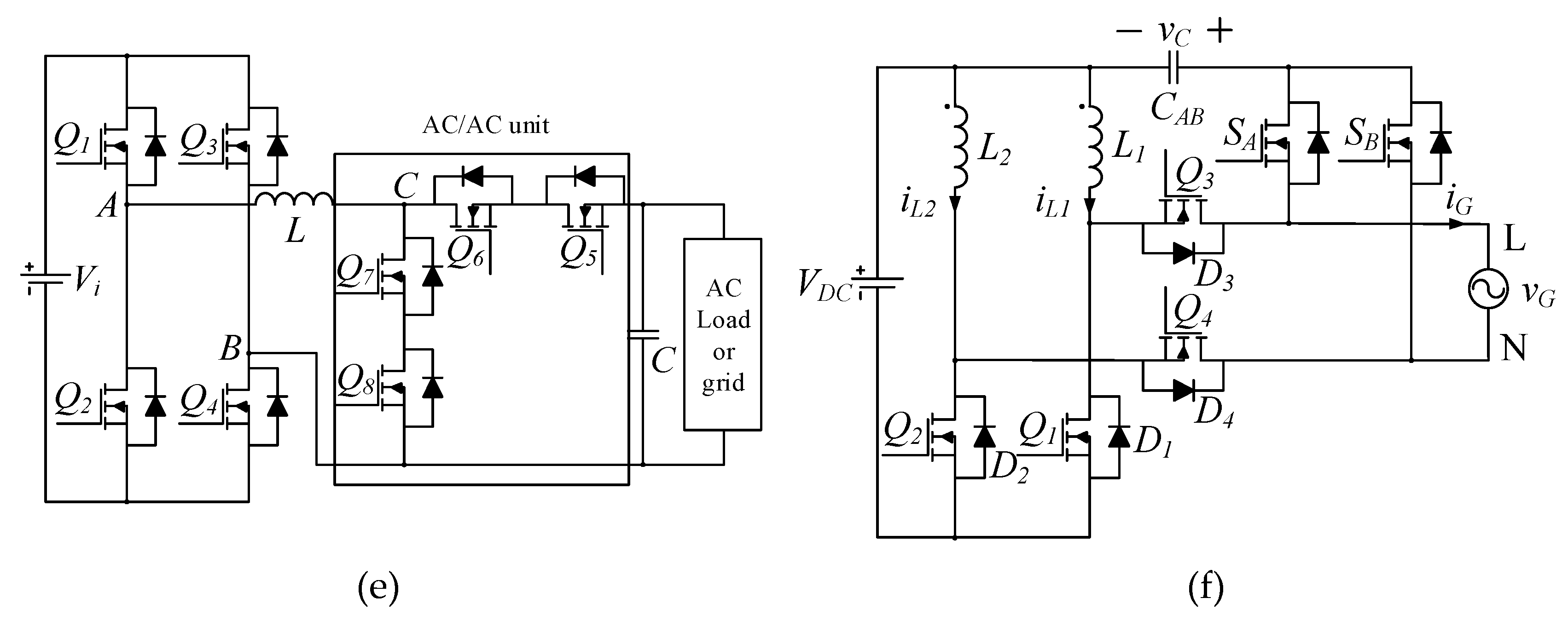
Additionally, due to the voltage step-up/down capability, the buck-boost derived topologies can also be a viable solution for single-stage inverter applications. Thus, a number of buck-boost type single-stage inverters with low component counts were reported. For instance, single-stage buck-boost inverters with only three switches were proposed in [4,5], as shown in Figure 1a, where a tapped inductor was used as a regular inductor in one half-line cycle and as a fly-back transformer in the subsequent half-line cycle. Unfortunately, this type of inverter cannot attain the required voltage step-up. As shown in Figure 1b, a four-switch, single-stage, buck-boost inverter was then presented in [6], which employed a tapped inductor and the SEPIC converter to increase the voltage gain. However, according to the operational principles, the turns ratio of the tapped inductor has to be equal to unity, and consequently, the voltage gain is still limited. Topologies in [7,8] also have only four switches to realize the single-stage conversion and have the merit of a common terminal between input and output ports. Figure 1c shows the circuit diagram of the converter in [7]. Another single-stage, buck-boost inverter has the advantage of reduced magnetic volume and low leakage currents [9]. The topologies in [10,11,12] were conceived to also eliminate the leakage currents, but the number of active switches is increased, as observed in Figure 1d. Furthermore, a differential buck-boost inverter with active power decoupling capability was proposed in [13,14], where no extra components are required. It has only four switches; on the contrary, a rather complicated control method is needed. An active buck-boost inverter using an “AC/AC unit” to realize the buck-boost conversion was introduced in [15,16], as presented in Figure 1e. Yet, each unit consisted of four switches, and, thus, in total, eight switches are needed for the microinverter. The authors of [17] expanded this idea to cascaded multilevel buck-boost inverters using H-bridges for each PV panel and a central AC/AC unit. To improve the efficiency and system reliability, a solution for the current shoot-through issue was discussed in [18,19] to eliminate the dead-time effect. Moreover, ref. [18] presented a converter with eight switches and four inductors, while [19] has four switches, four diodes, and six inductors, which make the topologies quite complicated. The topology in [20] has merits of a wide input voltage range, low leakage currents, small grid current ripples, and low common-mode voltages. However, as seen in Figure 1f, it has four high-frequency switches and two bidirectional switches, which are realized by connecting back-to-back MOSFETs in series. Doing so significantly increases the total number of switches (i.e., eight). Although the ideas of [4,5,6,7,8,9,10,11,12,13,14,15,16,17,18,19,20] are very interesting, their attained voltage gain is comparable to the traditional buck-boost converter.
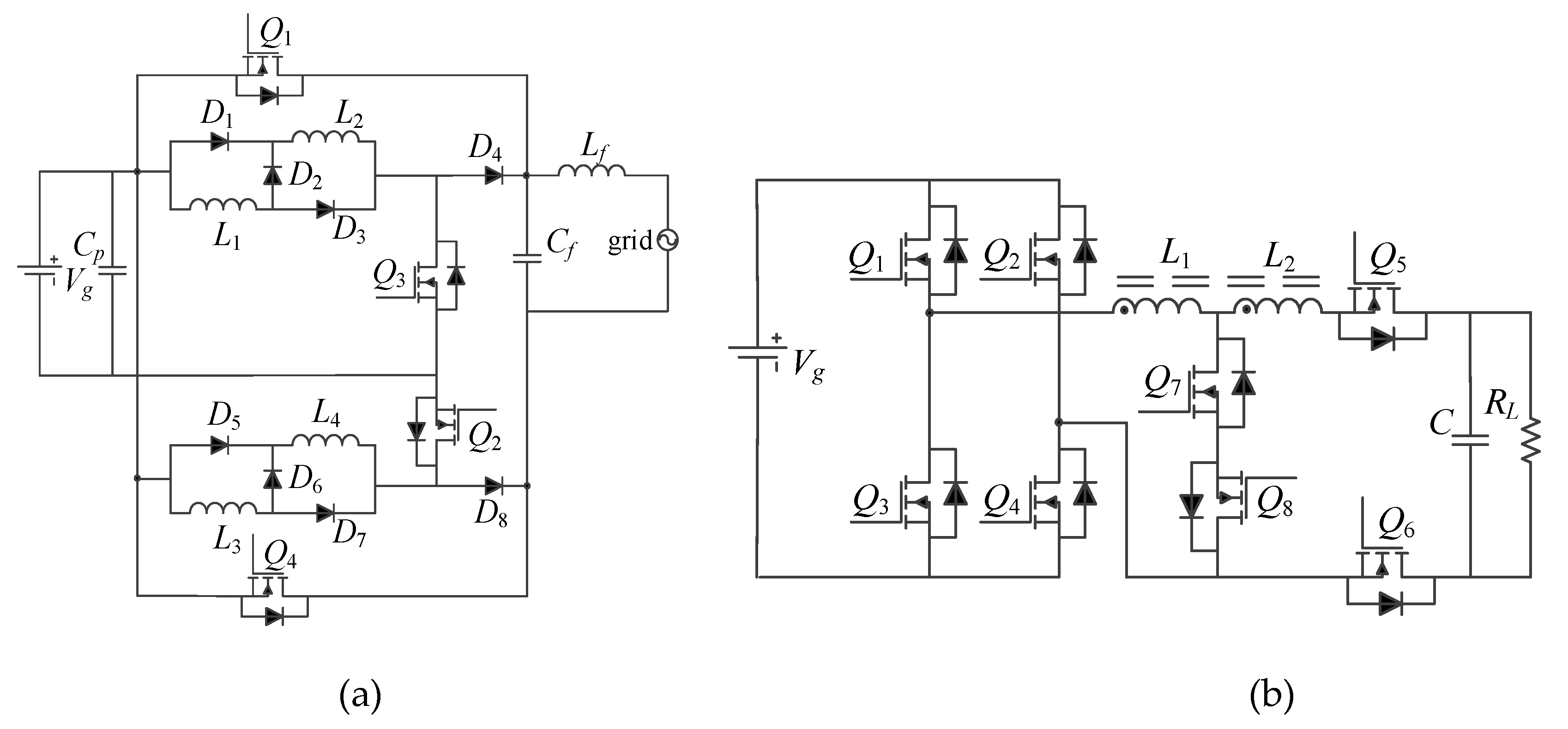
Additional attempts to increase the gain of the buck-boost derived topologies were reported. For example, in [21] a series connection between a buck-boost converter and the PV array was introduced to have a higher gain, but the gain improvement was limited. The topology in [22], see Figure 2a, employed a switched inductor, which can improve the gain by the factor of 2 over that of the traditional buck-boost converter. However, in total, the topology in [22] had four switches, eight diodes, and four inductors. The tapped-inductor buck-boost inverter topologies presented in [23,24], as shown in Figure 2b,c, respectively, can achieve a much higher voltage gain than the traditional ones, but the switch counts were up to eight, whereas [25,26] had five switches, as presented in Figure 2d. The advantage of the topologies in [25,26] is that only one high-frequency switch was used, and thus, the switching losses were lower. For the topologies in Figure 2, the main characteristics are further compared in Table 1. According to Table 1, most of the topologies had a high semiconductor count, from 7 up to 12. The experimental efficiency of more than 96% was reported in [23]. However, the test was with an input of 100–200 V and a 110-V output, which cannot support the performance with a high-voltage step-up. An efficiency of 86% was achieved in [25] with a 60-V input, a 230-V output, and 100-W output power, which is reasonable for a tapped-inductor buck-boost inverter. Yet, the experimental efficiency of the other two proposals was not reported clearly in the literature.
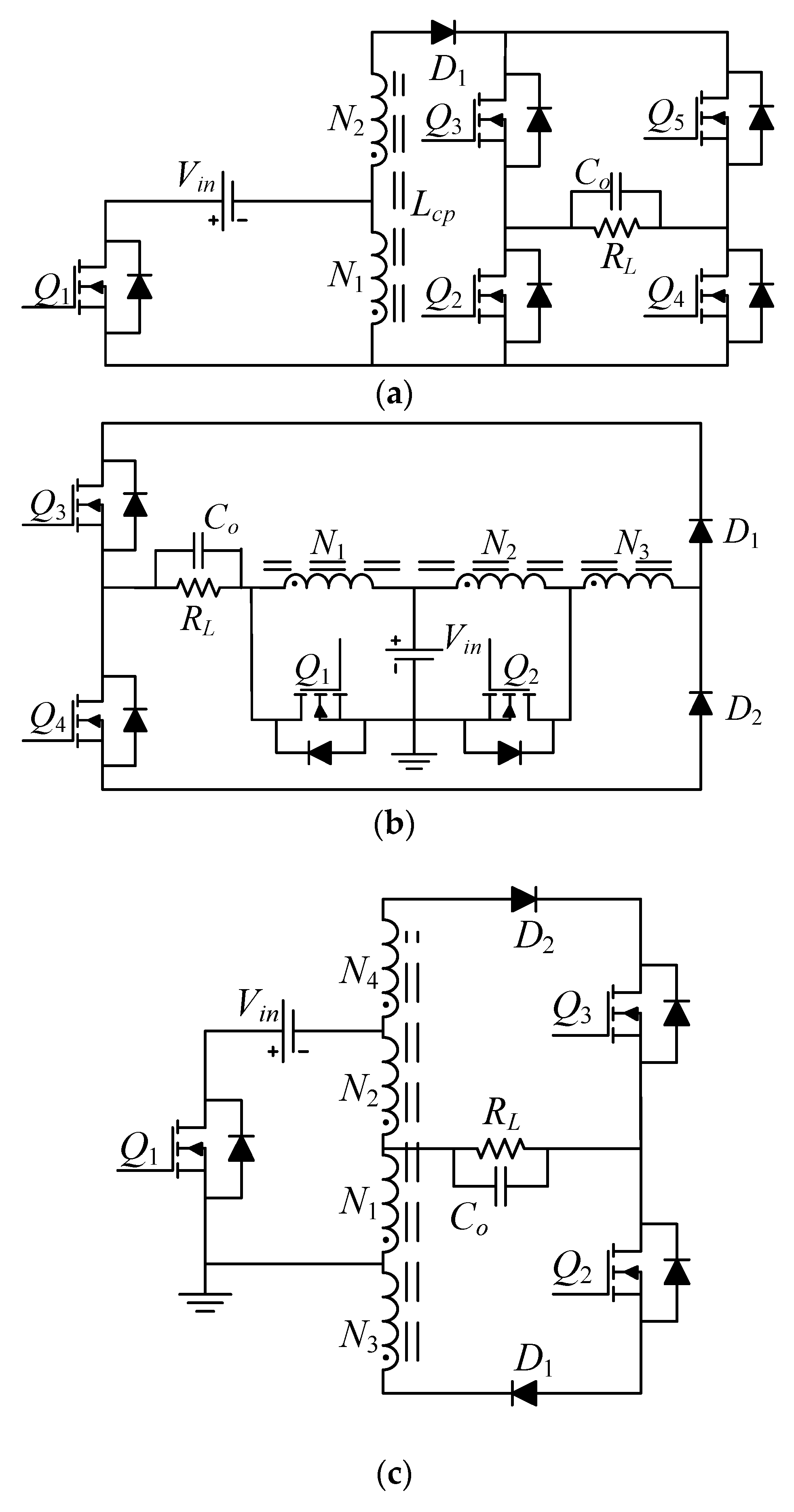
The high switch count of the reviewed converters, the resulting circuit complexity, higher cost, and lower efficiency, counter the main design goal of producing a simple and low-cost single-stage inverter. Therefore, more efforts have been made to develop more single-stage, buck-boost inverter topologies with a high gain and a low switch count. Recently, a family of single-stage, buck-boost rectifiers with high power factor were proposed in [27], analyzed, and verified in [28]. With the same principles, a family of tapped-inductor, buck-boost microinverters can be derived by reversing the power flow. This calls for the application of bidirectional switches. The proposed tapped-inductor, buck-boost type inverter family is illustrated in Figure 3. The basic operation and the preliminary simulation study of the two topologies in the family were reported in [29,30], while the converters have not been experimentally verified, and the design considerations are not fully addressed.
Accordingly, in addition to the topologies in [29,30], this paper further introduces two more practical topologies and all four topologies in the family are presented in detail. More importantly, a comparison of the proposed family was done thoroughly in terms of the component count, the voltage conversion ratio, the voltage stress, the peak current stress, and the RMS current stress, which can be used in the design phase. What is more, more detailed simulation studies for all the topologies in the family were presented. A prototype of the SSBBI of the proposed family was built and experimental results are illustrated in this paper. The rest of the paper is organized as follows. Section 2 introduces the proposed family, and the operation principles of the proposed family are demonstrated on a topology (i.e., the SSBBI) in Section 3. Circuit characteristics are discussed in Section 4, including the analysis of the conversion ratio, turns ratio, and duty cycle constraints together with voltage and current stresses, as design considerations. Simulation results are given in Section 5, where the comparison of the family is provided. Experimental tests are presented in Section 6 to validate the discussion. Finally, concluding remarks are provided in Section 7.

2. Single-Stage, Buck-Boost Inverter Family

As shown in Figure 3, the proposed inverter family makes use of a tapped inductor to attain a high step-up voltage conversion ratio. This helps to generate a grid-compatible voltage from a low DC voltage source. Two, three, and four winding, tapped-inductor structures are needed. The turns ratio, n, of the tapped inductor is defined as follows. For the two-windings inverter topology in Figure 3a, n = N2/N1. The three-windings topology in Figure 3b has an equal number of primary turns, N1 = N2, and the turns ratio is defined as n = N3/N1 = N3/N2. The topologies in Figure 3c,d rely on a symmetrical tapped-inductor structure with an equal turns ratio, defined as n = N3/N1 = N4/N2.
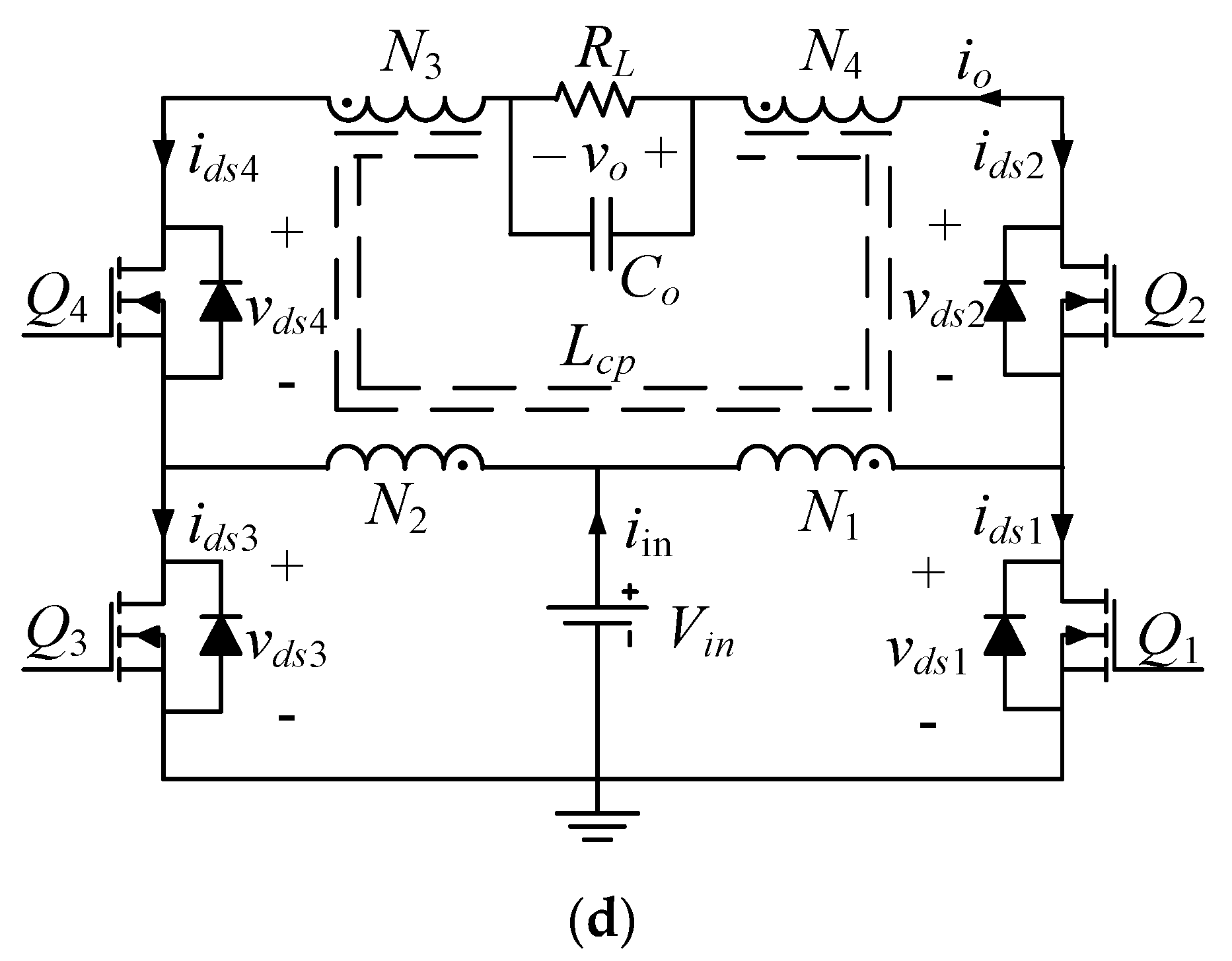
The topology in Figure 3a includes a floating source, a single ground-referenced PWM switch, Q1, and a ground-referenced line frequency unfolding bridge, Q2Q5. The topology in Figure 3b includes a grounded source, a ground-referenced push-pull pair of PWM switches, Q1Q2, and a floating line frequency unfolding totem pole, Q3Q4. The topology in Figure 3c includes a floating source, a single ground-referenced PWM switch, Q1, and a floating line frequency unfolding totem pole, Q2Q3. The topology in Figure 3d includes a grounded source and a ground-referenced full bridge. Here, the lower switches, Q1Q3, are PWM devices, whereas the high switch pair can perform either a simple line frequency unfolding function or be operated as synchronous rectifiers. Since the body diodes of the high switches are exploited as rectifiers, the reverse recovery capability should be considered. This can be an issue for silicon-based devices, while the emerging GaN MOSFETs can deliver the required performance.
To summarize, the proposed inverters have the merits of:
(1)
Generating a grid-level AC output voltage from a relatively low DC input voltage without extra high gain DC-DC converters.
(2)
Having a low component count as single-stage topologies consisting of a single magnetic device and three or four switches.
(3)
A push-pull or half/full-bridge arrangement of the switches, where the commercial low-cost driver-integrated circuits can be easily used.
The proposed tapped-inductor, buck-boost inverter family in Figure 3 was then studied through simulations. The exploration indicated that the topology in Figure 3d can also help to avoid much of the practical grounding, driving, and controller interface issues. Additionally, considering the lowest semiconductor count (see Table 2), the topology in Figure 3d appears as the most attractive candidate in the family. Hereafter, this topology (i.e., the SSBBI in Figure 3d) is considered in the following detailed analysis to exemplify the converter operation.

3. Operation Principles of the Proposed SSBBI

As shown in Figure 3d, the power stage of the proposed SSBBI included four switches, Q1Q4, in a full-bridge arrangement. A tapped inductor, Lcp, with four windings was employed. The output filter capacitor here was Co and the load was an equivalent resistance, RL, for stand-alone applications. The voltage across them was the AC output, vo. As mentioned previously, two symmetrical pairs of windings were used for the tapped inductor. The turns of the primary windings must be the same, i.e., N1 = N2. Similarly, equal secondary windings were used, i.e., N3 = N4. The turns ratio of the tapped inductor was then obtained as n = N3/N1 = N4/N2. The SSBBI can generate a bipolar output voltage with the help of the symmetrical structure, and thus, it can achieve the DC-AC inversion. The desired output voltage can be obtained using any common control strategy of a constant frequency duty cycle. The operation principle is detailed in the following.
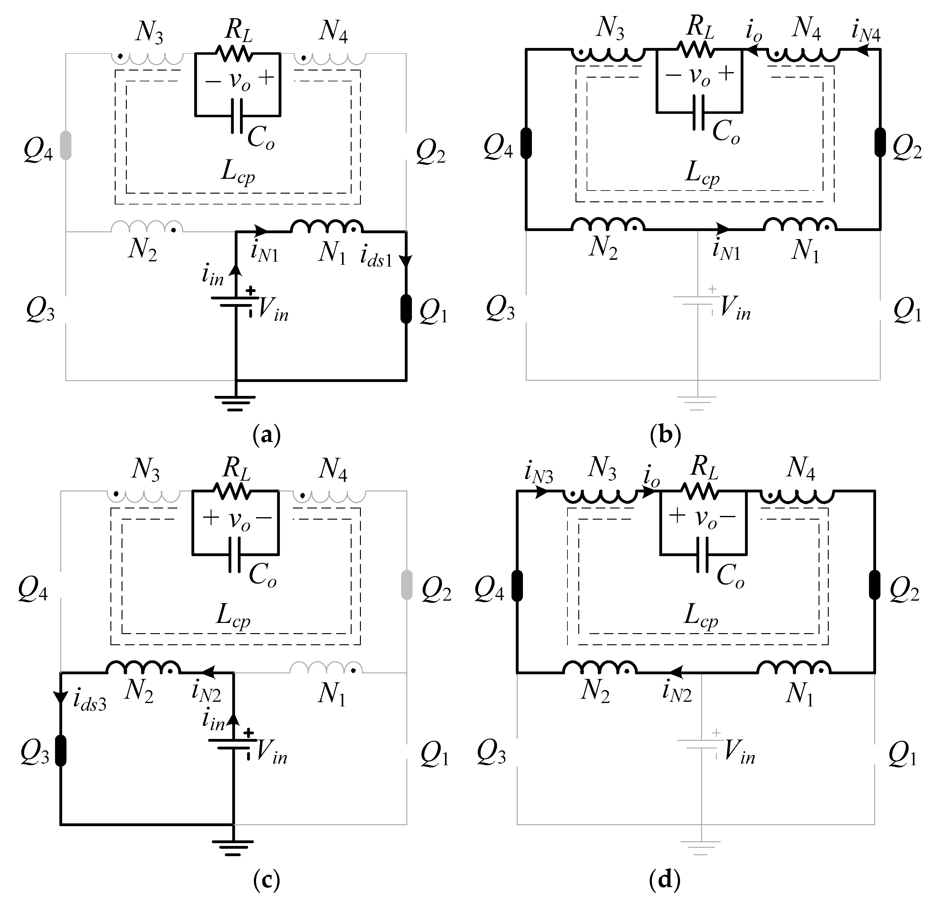
Supposing the converter was operating in the CCM, the SSBBI had two switching states in each half-line cycle, denoted as states A and B in the positive half-line cycle and A’ and B’ in the negative half-line cycle. The switching states of the four switches are listed in Table 3, and further illustrated in Figure 4.
According to the equivalent circuit of state A shown in Figure 4a, the state started at the beginning of each switching cycle in the positive half-line cycle. Here, the switch Q1 was turned on and the state lasted for the duration of DTs. In this state, the tapped inductor was charged by the input source, Vin, through the primary winding N1. The output capacitor, Co, can sustain the output voltage on the load. As shown in Figure 4b, state B began when the switch Q1 was turned off and lasted for the duration of (1 − D)Ts. In this state, the energy stored in the tapped inductor was discharged and released to the output side through all the four windings of the tapped inductor. During states A and B, when the output voltage was positive, Q1 and Q2 were switched, while the switch Q3 was maintained off and Q4 remained on. In comparison, the states A and B were replaced by the states A’ and B’ during the negative output half-line cycle due to the symmetrical operation principle. The equivalent circuits of state A’ and B’ are shown in Figure 4c,d, respectively.
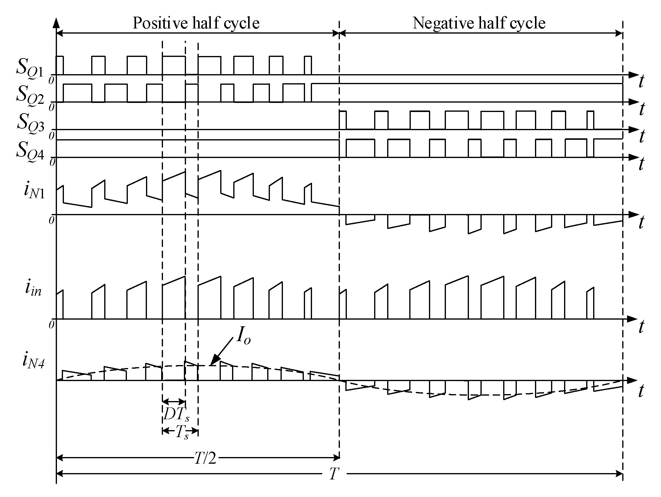
The key waveforms of the SSBBI are described in Figure 5, where SQ1SQ4 are the gating signals for Q1Q4 switches, respectively. Due to the symmetry of the SSBBI, it was sufficient to consider its operation during the positive half cycle. When Q1 was turned on and Q2 was turned off, the primary winding of the tapped inductor was energized. This caused the magnetizing current of the tapped inductor to ramp up. When Q1 was turned off and Q2 was turned on, the tapped inductor was discharged to support the output through all the windings. Thus, the magnetizing current of the tapped inductor ramped down. Notably, in terms of control of the converter, in grid-tied applications, the task of the control circuit is to shape the average output current, Io, into a sinusoidal waveform (see iN4 in Figure 5), while the controller should regulate the output voltage in stand-alone applications.

4. Analysis and Design Considerations of the Proposed SSBBI

4.1. CCM Voltage Gain

In the CCM, the tapped inductor, Lcp, was charged by the input voltage source, Vin, only through the primary winding N1 or N2 during the time of DTs (state A or A’). However, the output voltage, vo was stressed on all the four windings of the tapped inductor during the time of (1 − D)Ts (state B or B’). Thus, according to the volt-sec balance, it gives
0 D T s V i n d t + D T s T s v o 2 n + 2 d t = 0
which led to that the quasi-steady-state voltage gain of the SSBBI to be calculated as
M = v o V i n = 2 ( n + 1 ) D 1 D .
It can be recognized from Equation (2) that the SSBBI was a buck-boost type topology and had the function of voltage step-up/down. A higher gain can be achieved by choosing a proper turns ratio, n.

4.2. Turns Ratio and Duty Cycle Constraints

It should be noticed that when the tapped inductor is discharged to the output side (see states B and B’), the voltage across the primary winding must be always less than the DC input voltage, Vin. Accordingly,
v o 2 ( n + 1 ) < V i n .
In this way, it prevented the discharging current of the tapped inductor to go back to the DC input source through the body diode of the switch at the lower side. Such a condition should be avoided since the output voltage would be clamped and the circulating current will lower the efficiency as well. With this concern, the turns ratio should be designed sufficiently large to make the SSBBI work properly. Thus,
n > V o max 2 V i n 1 .
Moreover, it can be obtained by combining (2) and (3) that
D 1 D < 1 .
Subsequently, the maximum duty ratio, Dmax, should be limited to
D max < 0.5 .

4.3. Voltage and Current Stress

4.3.1. Voltage Stress of Switches

During state A, the input voltage, Vin, was imposed on the primary winding N1 of the tapped inductor when the switch Q1 was on. Therefore, the voltage stress on the switch Q3 was the sum of the input voltage and the induced voltage across the primary winding N2, which was twice the input voltage, Vin as
V Q 3 max = 2 V i n .
Meanwhile, since the switch Q4 was in on-state, the voltage across the four windings of the tapped inductor as well as the output voltage, vo, was stressed on the off-state switch Q2. Thus, the maximum stress of the Q2 will lead to:
V Q 2 max = 2 ( n + 1 ) V i n + V o max .
The same results can be obtained for the switches Q1 and Q4 in state A’ because of the symmetrical operation of the SSBBI. The voltage stresses for all the switches are summarized in Table 4.

4.3.2. Analysis of Current Stress

It was assumed that the output voltage and current of the SSBBI were ideally in phase without harmonics as
{ v o ( t ) = V m sin ω t i o ( t ) = I m sin ω t
Furthermore, by applying Equations (2) and (9), and replacing the steady-state duty ratio D with the time-varying duty ratio d(t), it can be obtained that
v o ( t ) V i n = 2 ( n + 1 ) d ( t ) 1 d ( t ) = V m sin ω t V i n
from which the duty ratio, d(t), can be derived as
d ( t ) = V m sin ω t 2 ( n + 1 ) V i n + V m sin ω t .
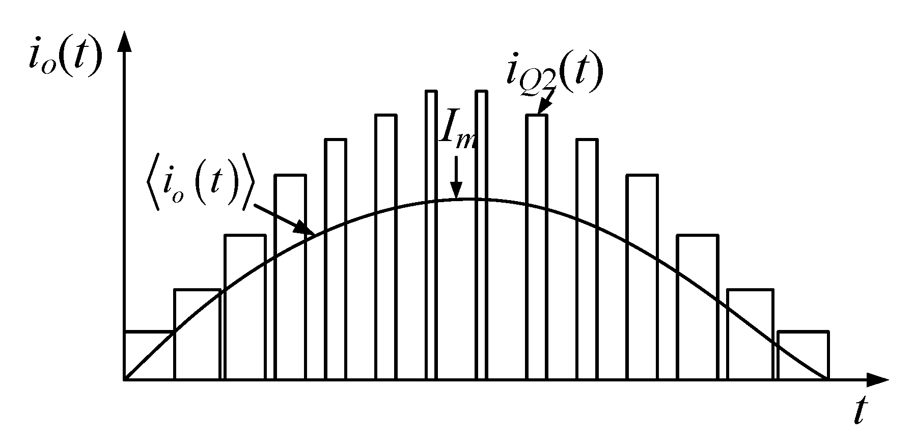
For the proposed SSBBI, the average output current equaled to the average current of the upper switch, 〈io(t)〉 = iQ2(t)[1 − d(t)], as shown in Figure 6. Therefore, assuming that the current ripples are negligible, the current amplitude of the switch Q2 can be obtained by combining Equations (9) and (11) as
i Q 2 ( t ) = i o ( t ) 1 d ( t ) = I m sin ω t + I m V m sin 2 ω t 2 ( n + 1 ) V i n .
Thus, the maximum current of the switch Q2 at the peak output voltage can be obtained as
I Q 2 max = I m + I m V m 2 ( n + 1 ) V i n .
The squared RMS current of the switch Q2 within a switching period is:
i Q 2 r m s T s 2 = 1 T s t t + T s i Q 2 2 ( t ) d t = [ 1 d ( t ) ] i Q 2 2 ( t ) .
Subsequently, the squared value of the switch RMS current is:
I Q 2 r m s 2 = 1 T / 2 0 T / 2 i Q 2 r m s T s 2 d t
with T being the generated output voltage period. Substituting Equations (11), (12), and (14) into (15) yields
I Q 2 r m s 2 = 1 T / 2 0 T / 2 I m 2 sin 2 ω t + I m 2 V m sin 3 ω t 2 ( n + 1 ) V i n d t = I a c r m s 2 ( 1 + 4 3 π V m ( n + 1 ) V i n ) .
Thus, the RMS current of the switch Q2 is obtained as
I Q 2 r m s = I a c r m s 1 + 4 3 π V m ( n + 1 ) V i n .
The current amplitude of the lower switch Q1 is 2(n + 1) times higher than the upper switch current due to the function of the tapped-inductor turns ratio, n. Thus,
i Q 1 ( t ) = 2 ( n + 1 ) i Q 2 ( t ) = 2 ( n + 1 ) I m sin ω t + I m V m sin 2 ω t V i n .
Therefore, the peak current through the lower switch, Q1, is:
i Q 1 max = 2 ( n + 1 ) I m + I m V m V i n .
The squared value of the lower switch RMS current through the switching period, Ts, is:
i Q 1 r m s T s 2 = 1 T s t t + T s i Q 1 2 ( t ) d t = d ( t ) i Q 1 2 ( t ) .
Since the low switch conducts for half the line period, the squared value of its RMS current on the line period scale can be calculated as:
I Q 1 r m s 2 = 1 T 0 T i Q 1 r m s T s 2 d t .
Substituting Equations (11), (18), and (20) into (21), gives
I Q 1 r m s = I a c r m s 3 8 V m 2 V g 2 + 8 3 π ( n + 1 ) V m V i n .
With the above analysis, the voltage and current stresses of the SSBBI are summarized in Table 4.

5. Simulation Results and Comparison

5.1. Basic System Operation

Referring to Figure 3d, simulations were carried out to verify the feasibility of the proposed SSBBI in PSIM software. The key simulation parameters were: Output power Po = 200 W, input voltage Vin = 48 V, output voltage vo = 110 V/60 Hz, switching frequency fs = 20 kHz, tapped-inductor magnetizing inductance Lm = 150 μH, turns ratio n = 1.5, and output capacitance Co = 2 μF. Several control strategies can be applied to control the proposed SSBBI. Initially, to validate the basic operational principle, the simple open-loop SPWM was used. Simulation results are shown in Figure 7, which demonstrates that the SSBBI can generate the desired output voltage. This provides proof of concept of the proposed circuit family for single-stage microinverter applications.
Furthermore, as can be observed in Figure 7a, the circuit simulation results (key waveforms) were in a close agreement with the analytical results in Figure 5. The gate-driving signals are further shown in Figure 7b to demonstrate the controllability of the converter. Moreover, the output voltage of the proposed inverter is given in Figure 7c, as well as the voltage across the switches. It can be observed in Figure 7c that the SSBI can produce high-quality sinusoidal outputs, and the voltage stresses on the switches were also in consistency with the analysis. Additionally, the currents flowing through the power devices under the 200-W output power are presented in Figure 7d, which again agrees with the theoretical analysis presented in Section 4.
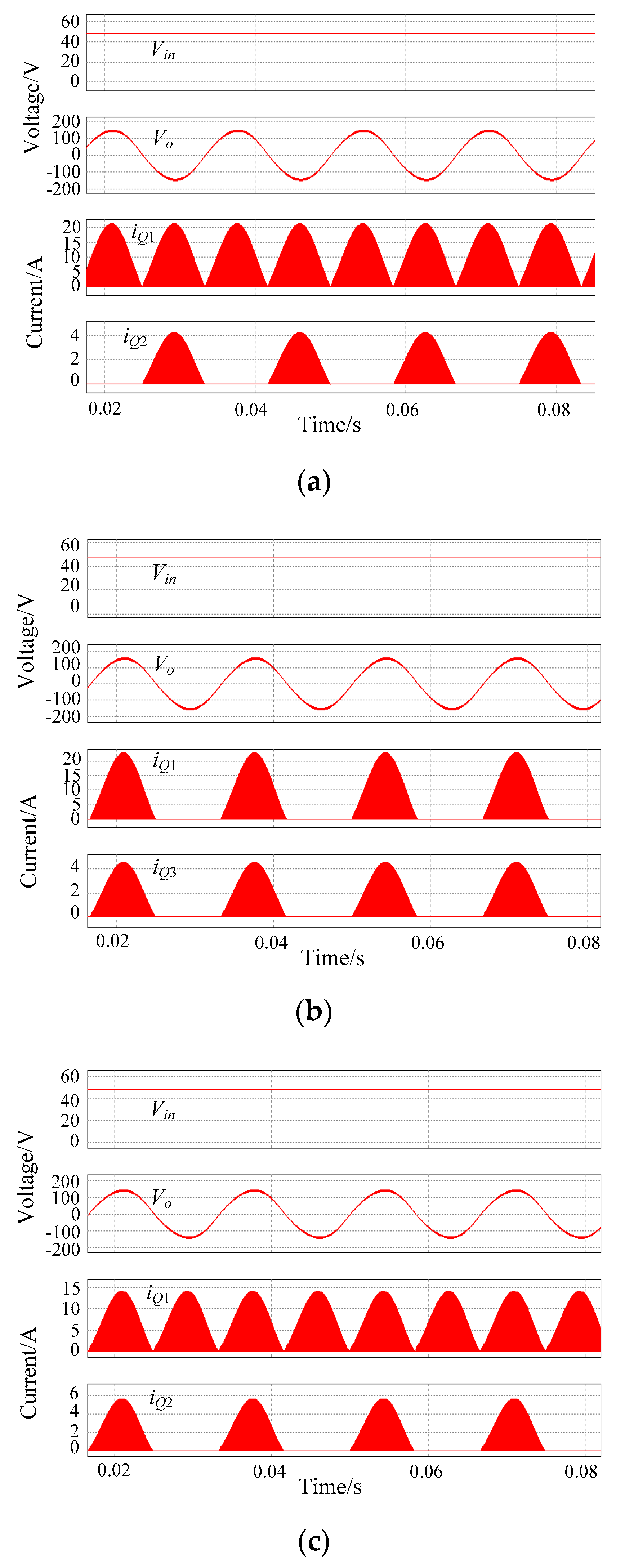
The analytical results were further verified by simulations. Key simulated waveforms of the proposed topologies in Figure 3a–c are shown in Figure 8. It is observed in Figure 8 that all the topologies of the proposed family can generate a good-quality sinusoidal output voltage. Simulations also support the theoretically predicted results of the current stress analysis. When comparing the performance of the topologies in Figure 3a–c with the SSBBI, it can be seen that the four topologies had similar high-quality output voltage waveforms and the comparable current stress at the same output power. However, the SSBBI had the lowest semiconductor count and the easier driver implementation, which proved again the competitiveness of the SSBBI in the family.

5.2. Comparison of the Proposed Single-Stage, Buck-Boost Inverter Family

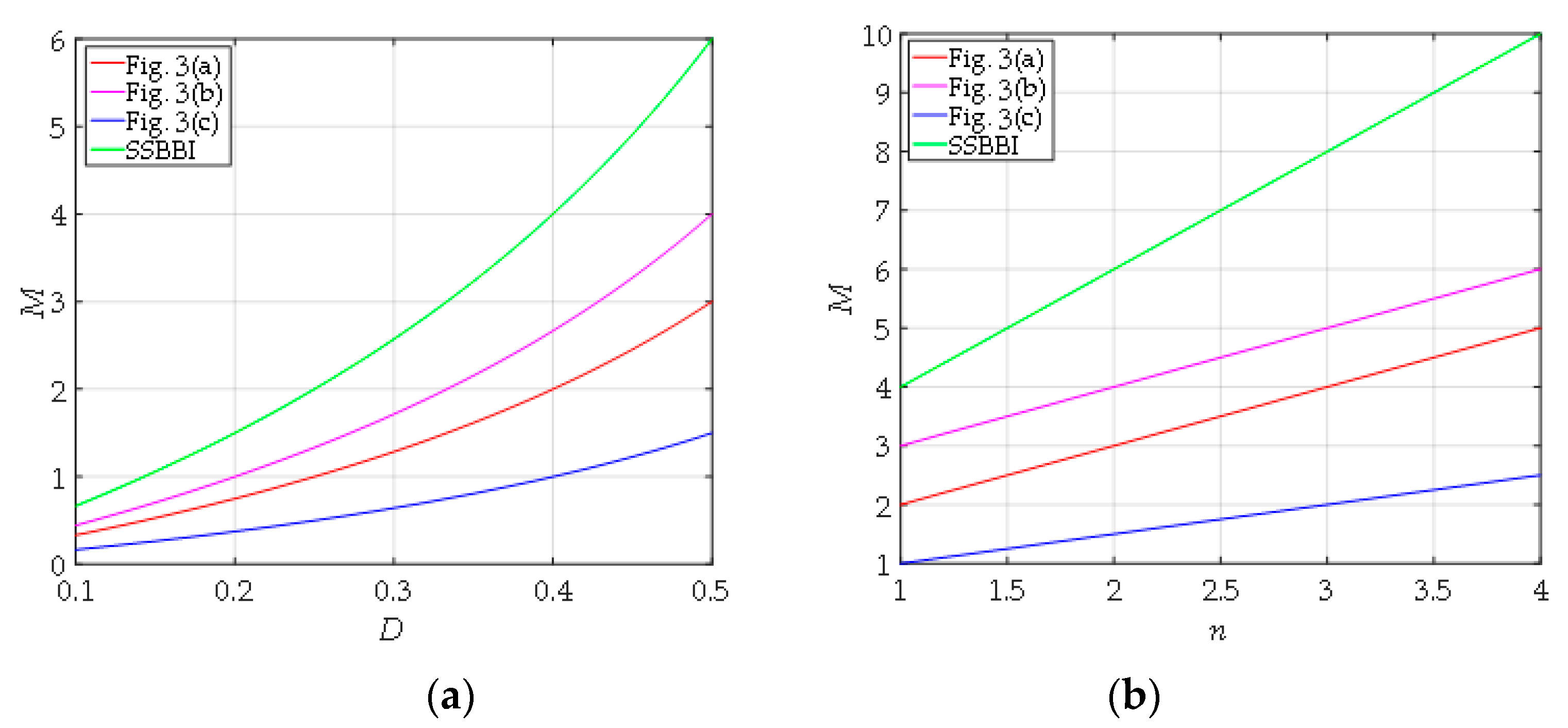
To better appreciate the merits of the proposed single-stage inverter family, a detailed comparison of the proposed topologies is conducted in this section. The voltage conversion ratio of the proposed family and its derivation under the assumption of the CCM operation is summarized in Table 5. The benchmarking of the proposed topologies’ voltage conversion ratio with the same turns ratio n = 2 is further shown in Figure 9a and with the same duty ratio D = 0.5 in Figure 9b. According to Table 5 and Figure 9, the SSBBI had the largest voltage gain in the family. The peak voltage stress analysis was performed and is summarized in Table 6. Lastly, Table 7 and Table 8 present the results of the peak current and the RMS current stress analysis of semiconductor devices. As can be seen from Table 6, Table 7 and Table 8, the voltage and current stresses of the SSBBI were comparable to other topologies in the family. Moreover, as mentioned previously, the SSBBI component count was lower by one or two diodes. Thus, the SSBBI had the optimum circuit composition and characteristics in the family.

6. Experimental Results and Discussion

6.1. Experimental Results of SSBBI

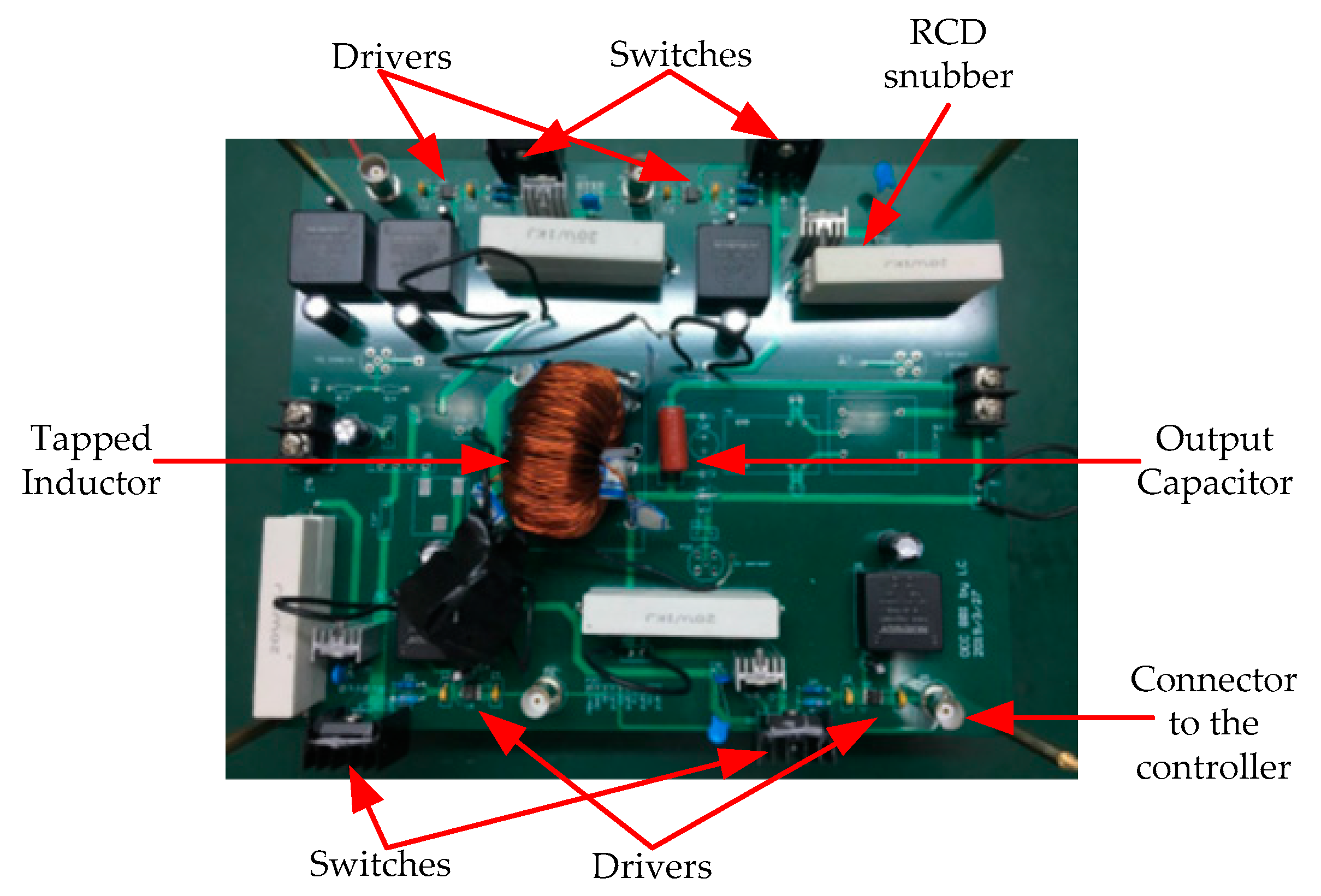
A 100-W laboratory prototype of the proposed SSBBI was built and tested. The key operation parameters were: Input voltage, Vin = 48 V; output voltage, vo = 110 V/60 Hz; and switching frequency, fs = 20 kHz. The prototype’s view and the components arrangement are shown in Figure 10. The board was designed larger to reserve additional space needed for experimenting with various snubbers and control schemes. The main components of the prototype are summarized in Table 9. The tapped inductor was designed according to the design guide provided by Magnetics-Inc [31], including the magnetic core, the turns, and the wire. A dSPACE system was used to implement the control for the quick experimental study of the SSBBI.
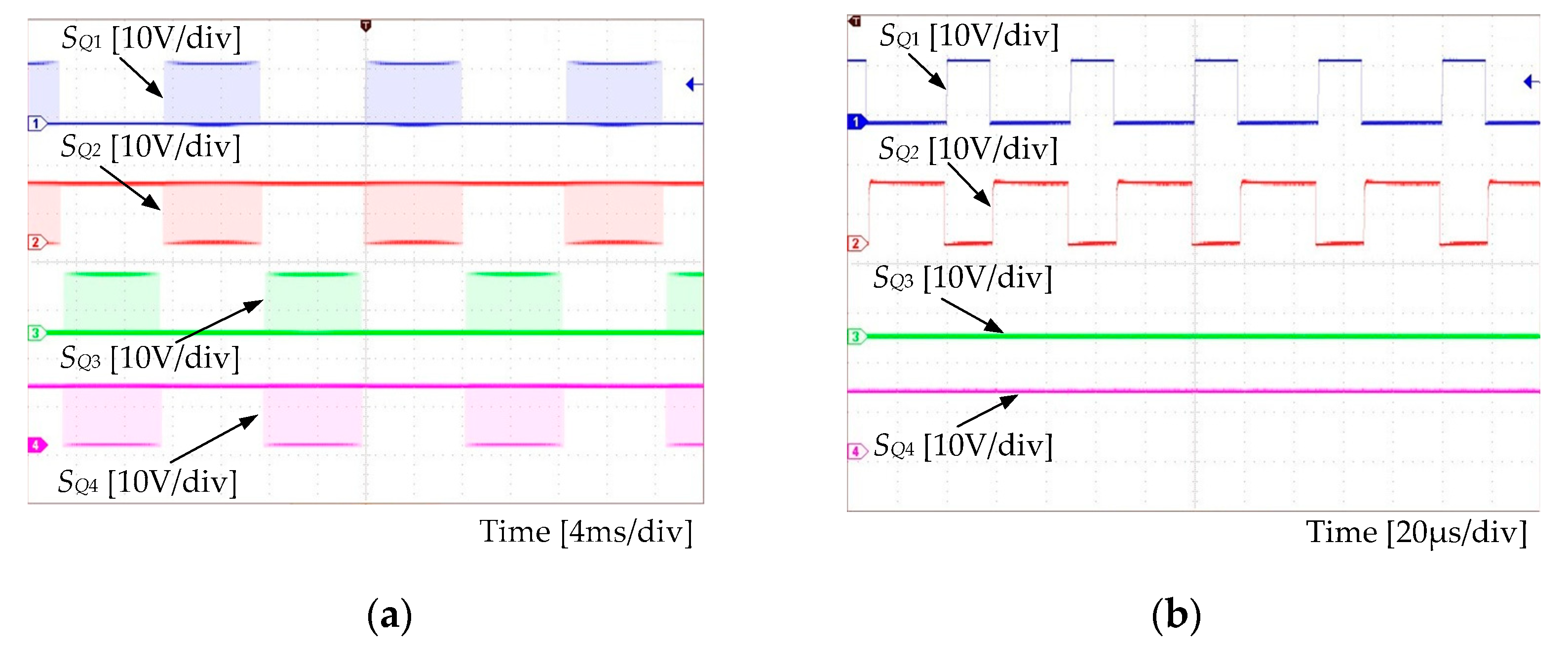
Experimental results are shown in Figure 11 and Figure 12. Figure 11 presents the gate-driving signals for switches at the line period scale and at the switching period scale, respectively. The output voltage and the switch voltage are shown in Figure 12. Observations in Figure 12 clearly indicate that the output voltage was sinusoidal. The THD of the experimental output voltage was around 5% with the open-loop control. This verified that the experimental SSBBI prototype operated according to the theoretical expectations. That is, the proposed SSBBI can achieve the inversion and produce a high-quality sinusoidal output.
In addition, as shown in Figure 12, when zooming into the switch voltage waveform, it was revealed that a voltage spike appeared at the instant of the switch turning off. This is typical for converters with coupled inductors [32]. For the first version of the prototype, a simple RCD snubber was used to verify the basic operation principle of the proposed topologies. The efficiency of 75% was achieved with 100-W output power, where the RCD snubber accounted for a large portion of the total power losses. Moreover, the voltage spike can be suppressed with an appropriate snubber arrangement and design to capture and recycle the leakage energy to achieve much higher efficiency according to the analysis. Snubber details and verification are the subjects of the follow-up research work. What is more, the voltage gain was slightly lower than the theoretical one due to the power losses. With the planned regenerative snubber, the power losses will be less and, thus, the practical voltage gain should be closer to the theoretical one. Overall, the simulation and experimental results were in agreement with the theoretical analysis. Thus, the effectiveness of the proposed inverter family was verified, which had the merits of single-stage conversion, low component count, and easy implementation. These advantages are significant from PV applications, while the efficiency should be further enhanced.

6.2. Comparison of the SSBBI and the State of the Art

After the preliminary experimental test of the SSBBI prototype, the non-optimized performance of the SSBBI could be compared with its counterparts. The comparison results are shown in Table 10. According to Table 10, it is known that the SSBBI had the lowest semiconductor count, almost half of its counterparts. The lower component count makes the SSBBI a simple structure, requiring simpler driving and auxiliary power supplies. These advantages will lead to lower cost, which is a practical concern for the microinverters.
The efficiency performance of the SSBBI was not outperforming, as mentioned previously. With the theoretical analysis and simulations, the power losses on the RCD snubber were around 15%. Thus, with a proper regenerative snubber, the efficiency will be more than 85% as predicted, where component optimization can further be applied to improve the efficiency. Nevertheless, the efficiency of 85% will be reasonable for a 100-W, single-stage, buck-boost inverter and comparable with the experimental efficiency in [25].

7. Conclusions

This paper introduced a family of single-stage, buck-boost inverter topologies. Compared to the counterparts, the proposed topologies had a lower component count. The key feature of the proposed family was the application of a multi-winding tapped inductor that helped to attain a higher voltage gain required in PV applications, as microinverters. The operational principle was discussed in this paper, which was supported by simulation and experimental results. A stand-alone experimental SSBBI prototype was designed, built, and tested. Experimental results showed that the proposed topology is capable of delivering a well-shaped sinusoidal output. However, the practical voltage gain was slightly lower than theoretical prediction and the efficiency was not at a very satisfactory level due to the RCD snubber losses and the un-optimized components of the converter, which will be the future work. Overall, the proposed family can present a viable solution to single-stage microinverter applications.

Author Contributions

Conceptualization, A.A.; methodology, A.A. and B.Z.; software, B.Z.; validation, C.L., B.Z., and Y.H.; formal analysis, B.Z.; investigation, C.L.; resources, Y.H.; data curation, C.L.; writing—original draft preparation, B.Z.; writing—review and editing, A.A and Y.Y.; visualization, Y.Y.; supervision, Y.H.; project administration, B.Z.; funding acquisition, B.Z. All authors have read and agreed to the published version of the manuscript.

Funding

This research was funded by the National Natural Science Foundation of China under Grant No. 51807164 and by Shaanxi Key R&D Program under Grant No. 2018GY-073 and by Xi’an Science and Technology Association Youth Talent Support Project.

Conflicts of Interest

The authors declare no conflict of interest.

Nomenclature

nTurns ratio of the tapped inductor
N1, N2, N3, N4Windings of the tapped inductor
Q1, Q2, Q3, Q4, Q5Switches (MOSFETs)
D1, D2Diodes
LcpTapped inductor
RLEquivalent load resistance
CoOutput capacitor
VinInput voltage
iinInput current
voOutput voltage
ioOutput current
vds1, vds2, vds3, vds4Drain-source voltage of the switches Q1Q4
ids1, ids2, ids3, ids4Currents through the switches Q1Q4
DDuty cycle
TsSwitching period
iN1, iN2, iN3, iN4Currents through the windings
SQ1, SQ2, SQ3, SQ4Gating signals the switches Q1Q4
IoAverage output current
MVoltage gain
VomaxMaximum output voltage
DmaxMaximum duty ratio
VQ1max, VQ2 max, VQ3 max, VQ4 maxVoltage stress on the switches Q1Q4
vo(t)Time-varying output voltage
io(t)Time-varying output current
VmPeak output voltage
ImPeak output current
ωAngular frequency
d(t)Time-varying duty ratio
IQ1max, IQ2maxMaximum current of the switch Q1, Q2
i Q 1 r m s T s 2 , i Q 2 r m s T s 2 Squared RMS current of the switch Q1, Q2 within a switching period
I Q 1 r m s 2 , I Q 2 r m s 2 Squared RMS current of the switch Q1, Q2
IQ1rms, IQ2rmsRMS current of the switch Q1, Q2
fsSwitching frequency
LmTapped-inductor magnetizing inductance

Abbreviations

DCDirect current
ACAlternating current
PV
MIE/MIC
Photovoltaic
Module-integrated electronic/converter
MPPTMaximum power point tracking
SEPICSingle ended primary inductor converter
PWM
MOSFET
Pulse width modulation
Metal oxide semiconductor field-effect transistor
GaNGallium nitride
SSBBISingle-stage, buck-boost inverter
CCMContinuous conduction mode
SPWMSinusoidal pulse width modulation
THD
RMS
Total harmonic distortion
Root mean square
RCDResistor-capacitor-diode

References

  1. Meneses, D.; Blaabjerg, F.; Garcia, O.; Cobos, J.A. Review and comparison of step-up transformerless topologies for photovoltaic AC-module application. IEEE Trans. Power Electron. 2013, 28, 2649–2663. [Google Scholar] [CrossRef] [Green Version]
  2. Fang, Y.; Ma, X. A novel PV microinverter with coupled inductors and double-boost topology. IEEE Trans. Power Electron. 2010, 25, 3139–3147. [Google Scholar] [CrossRef]
  3. Abramovitz, A.; Zhao, B.; Smedley, K.M. High-gain single-stage boosting inverter for photovoltaic applications. IEEE Trans. Power Electron. 2016, 31, 3550–3558. [Google Scholar] [CrossRef]
  4. Zhang, Y.; Woldegiorgis, A.T.; Chang, L. Design and test of a novel buck-boost inverter with three switching devices. In Proceedings of the 2012 Twenty-Seventh Annual IEEE Applied Power Electronics Conference and Exposition (APEC), Orlando, FL, USA, 5–9 February 2012. [Google Scholar]
  5. Chowdhury, A.S.K.; Chakraborty, S.; Salam, K.M.A.; Razzak, M.A. Design of a single-stage grid-connected buck-boost photovoltaic inverter for residential application. In Proceedings of the 2014 Power and Energy Systems: Towards Sustainable Energy, Bangalore, India, 13–15 March 2014. [Google Scholar]
  6. Kumar, A.; Gautam, V.; Sensarma, P. A SEPIC derived single-stage buck-boost inverter for photovoltaic applications. In Proceedings of the 2014 IEEE International Conference on Industrial Technology (ICIT), Busan, Korea, 26 February–1 March 2014. [Google Scholar]
  7. Kumar, A.; Sensarma, P. A four-switch single-stage single-phase buck-boost inverter. IEEE Trans. Power Electron. 2017, 32, 5282–5292. [Google Scholar] [CrossRef]
  8. Kumar, A.; Sensarma, P. New switching strategy for single-mode operation of a single-stage buck-boost inverter. IEEE Trans. Power Electron. 2018, 33, 5927–5936. [Google Scholar] [CrossRef]
  9. Akbar, F.; Cha, H.; Lee, S.; Nguyen, T. A single-phase transformerless buck-boost inverter for standalone and grid-tied applications with reduced magnetic volume. In Proceedings of the 2019 10th International Conference on Power Electronics and ECCE Asia (ICPE 2019-ECCE Asia), Busan, Korea, 27–30 May 2019. [Google Scholar]
  10. Mostaan, A.; Abdelhakim, A.; Soltani, M.; Blaabjerg, F. Single-phase transformer-less buck-boost inverter with zero leakage current for PV systems. In Proceedings of the 2017 43rd Annual Conference of the IEEE Industrial Electronics Society (IECON), Beijing, China, 29 October–1 November 2017. [Google Scholar]
  11. Muhammedali Shafeeque, K.; Subadhra, P.R. A novel single-stage DC-AC boost inverter for solar power extraction. In Proceedings of the 2013 Annual International Conference on Emerging Research Areas and 2013 International Conference on Microelectronics, Communications and Renewable Energy, Kanjirapally, India, 4–6 June 2013. [Google Scholar]
  12. Wu, W.; Ji, J.; Blaabjerg, F. Aalborg inverter -a new type of “buck in buck, boost in boost” grid-tied inverter. IEEE Trans. Power Electron. 2015, 30, 4784–4793. [Google Scholar] [CrossRef]
  13. Xu, S.; Chang, L.; Shao, R.; Mohomad, A.R.H. Power decoupling method for single-phase buck-boost inverter with energy-based control. In Proceedings of the 2017 IEEE Applied Power Electronics Conference and Exposition (APEC), Tampa, FL, USA, 26–30 March 2017. [Google Scholar]
  14. Xu, S.; Shao, R.; Chang, L.; Mao, M. Single-phase differential buck-boost inverter with pulse energy modulation and power decoupling control. IEEE J. Emerg. Sel. Top. Power Electron. 2018, 6, 2060–2072. [Google Scholar] [CrossRef]
  15. Tang, Y.; Dong, X.; He, Y. Active buck-boost inverter. IEEE Trans. Ind. Electron. 2014, 61, 4691–4697. [Google Scholar] [CrossRef]
  16. Tang, Y.; Xu, F.; Bai, Y.; He, Y. Comparative analysis of two modulation strategies for an active buck-boost inverter. IEEE Trans. Power Electron. 2016, 31, 7963–7971. [Google Scholar] [CrossRef]
  17. Huang, Q.; Huang, A.Q.; Yu, R.; Liu, P.; Yu, W. High-efficiency and high-density single-phase dual-mode cascaded buck-boost multilevel transformerless PV inverter with GaN AC switches. IEEE Trans. Power Electron. 2019, 34, 7474–7488. [Google Scholar] [CrossRef]
  18. Khan, A.A.; Cha, H.; Ahmed, H.F.; Kim, J.; Cho, J. A highly reliable and high-efficiency quasi single-stage buck-boost inverter. IEEE Trans. Power Electron. 2017, 32, 4185–4198. [Google Scholar] [CrossRef]
  19. Khan, A.A.; Cha, H. Dual-buck-structured high-reliability and high-efficiency single-stage buck-boost inverters. IEEE Trans. Ind. Electron. 2018, 65, 3176–3187. [Google Scholar] [CrossRef]
  20. Ho, C.N.M.; Siu, K.K.M. Manitoba inverter---single-phase single-stage buck-boost VSI topology. IEEE Trans. Power Electron. 2019, 34, 3445–3456. [Google Scholar] [CrossRef]
  21. Testa, A.; Caro, S.D.; Scimone, T.; Panarello, S. A buck-boost based DC/AC converter for residential PV applications. In Proceedings of the International Symposium on Power Electronics, Electrical Drives, Automation and Motion, Sorrento, Italy, 20–22 June 2012. [Google Scholar]
  22. Abdel-Rahim, O.; Orabi, M.; Ahmed, M.E. Buck-boost interleaved inverter for a grid-connected photovoltaic system. In Proceedings of the 2010 IEEE International Conference on Power and Energy, Kuala Lumpur, Malaysia, 29 November–1 December 2010. [Google Scholar]
  23. Tang, Y.; He, Y.; Dong, X. Active buck-boost inverter with coupled inductors. In Proceedings of the 2014 IEEE Energy Conversion Congress and Exposition (ECCE), Pittsburgh, PA, USA, 14–18 September 2014. [Google Scholar]
  24. Husev, O.; Matiushkin, O.; Roncero-Clemente, C.; Blaabjerg, F.; Vinnikov, D. Novel family of single-stage buck-boost inverters on the unfolding circuit. IEEE Trans. Power Electron. 2019, 34, 7662–7676. [Google Scholar] [CrossRef]
  25. Sreekanth, T.; Lakshminarasamma, N.; Mishra, M.K. Coupled inductor-based single-stage high gain DC-AC buck-boost inverter. IET Power Electron. 2016, 9, 1590–1599. [Google Scholar] [CrossRef]
  26. Sreekanth, T.; Lakshminarasamma, N.; Mishra, M.K. A single-stage grid-connected high gain buck-boost inverter with maximum power point tracking. IEEE Trans. Energy Convers. 2017, 32, 330–339. [Google Scholar] [CrossRef]
  27. Zhao, B.; Abramovitz, A.; Smedley, K. Family of bridgeless buck-boost PFC rectifiers. IEEE Trans. Power Electron. 2015, 30, 6524–6527. [Google Scholar] [CrossRef]
  28. Zhao, B.; Ma, R.; Abramovitz, A.; Smedley, K. Bridgeless buck-boost PFC rectifier with a bi-directional switch. In Proceedings of the 2016 IEEE 8th International Power Electronics and Motion Control Conference (IPEMC-ECCE Asia), Hefei, China, 22–26 May 2016. [Google Scholar]
  29. Zhao, B.; Abramovitz, A.; Ma, R.; Huangfu, Y. High gain single stage buck-boost inverter. In Proceedings of the 2017 20th International Conference on Electrical Machines and Systems (ICEMS), Sydney, Australia, 11–14 August 2017. [Google Scholar]
  30. Zhao, B.; Abramovitz, A.; Ma, R.; Liang, B. One-cycle-controlled high gain single stage buck-boost inverter for photovoltaic application. In Proceedings of the 43rd Annual Conference of the IEEE Industrial Electronics Society (IECON), Beijing, China, 29 October–1 November 2017. [Google Scholar]
  31. Design Guide of Inductor. Available online: www.mag-inc.com (accessed on 10 January 2020).
  32. Abramovitz, A.; Smedley, M.K. Analysis and design of a tapped-inductor buck-boost PFC rectifier with low bus voltage. IEEE Trans. Power Electron. 2011, 26, 2637–2649. [Google Scholar] [CrossRef]
Figure 1. Prior-art, single-stage, buck-boost inverters: (a) [5], (b) [6], (c) [7], (d) [12], (e) [15], and (f) [20].
Energies 13 01675 g001aEnergies 13 01675 g001b
Figure 2. Prior-art, single-stage, buck-boost inverters with high gains: (a) [22], (b) [23], (c) [24], and (d) [25].
Energies 13 01675 g002aEnergies 13 01675 g002b
Figure 3. Proposed family of single-stage, buck-boost inverters: (a) Variant 1, (b) Variant 2, (c) Variant 3, (d) Variant 4 (SSBBI).
Energies 13 01675 g003aEnergies 13 01675 g003b
Figure 4. Equivalent circuits (switching states) of the proposed SSBBI: (a) State A, (b) State B, (c) State A’, (d) State B’.
Energies 13 01675 g004
Figure 5. Illustration of key waveforms of the proposed SSBBI.
Energies 13 01675 g005
Figure 6. Illustration of the switch current, iQ(t), and the average output current, <io(t)>, throughout the half-line cycle.
Energies 13 01675 g006
Figure 7. Key simulation waveforms of the proposed SSBBI: (a) Driving signal and currents on the switching period scale; (b) driving signals for switches; (c) Vds of the switches in one leg, input, and output voltage; (d) switch currents on the output period scale.
Energies 13 01675 g007
Figure 8. Simulation waveforms of the input voltage, output voltage, and switches’ current of the variant topologies: (a) Figure 3a, (b) Figure 3b, (c) Figure 3c.
Energies 13 01675 g008
Figure 9. Comparison of the voltage conversion ratio, M, of the proposed single-stage inverter family: (a) As function of the duty ratio D (for n = 2), (b) as function of the turn ratio n (for D = 0.5).
Energies 13 01675 g009
Figure 10. Photo of the experimental prototype of the proposed SSBBI.
Energies 13 01675 g010
Figure 11. SSBBI’s driving signals: (a) At the line period scale, (b) during positive half-line cycle (at switching period scale), (c) negative half-line cycle (at switching period scale).
Energies 13 01675 g011aEnergies 13 01675 g011b
Figure 12. Experimental waveforms of Vds2, Vds1, Vin, and vo: (a) At the line period scale, (b) at the switching period scale.
Energies 13 01675 g012
Table 1. Comparison of the main topologies of the existing single-stage, buck-boost inverters.
Ref.Switches CountDiodes CountInductors CountInput VoltageOutput VoltageOutput PowerEfficiency
[22]48420 V314 V100 W/
[23]801 Tapped100–200 V110 V500 W>96%
Figure 2b [24]801 Tapped40 V230 V//
[25]521 Tapped60 V230 V100 W86%
Table 2. Comparison of the component count of the tapped-inductor, buck-boost inverter family.
TopologiesSwitchesDiodesWindingsFilter Cap.
Figure 3a5121
Figure 3b4231
Figure 3c3241
Figure 3d4041
Table 3. Switching states of semiconductor devices.
SwitchesPositive Output VoltageNegative Output Voltage
State AState BState A’State B’
Q1OnOffOffOff
Q2OffOnOnOn
Q3OffOffOnOff
Q4OnOnOffOn
Table 4. SSBBI switch voltage and current stresses.
SwitchesVoltage StressCurrent Stress
PeakRMS
Q1, Q32Vin 2 ( n + 1 ) I m + I m V m V i n I a c r m s 3 8 V m 2 V i n 2 + 8 3 π ( n + 1 ) V m V i n
Q2, Q42(n+1)Vin+Vomax I m + I m V m 2 ( n + 1 ) V i n I a c r m s 1 + 4 3 π V m ( n + 1 ) V i n
Table 5. Comparison of the voltage conversion ratio of the proposed topologies.
TopologyVoltage Gain M = vo/Vin
Figure 3a M a = ( n + 1 ) D 1 D
Figure 3b M b = ( n + 2 ) D 1 D
Figure 3c M c = ( n + 1 ) 2 D 1 D
SSBBI M = 2 ( n + 1 ) D 1 D
Table 6. Comparison of the voltage stress.
TopologyVoltage Stress
Low Side SwitchesHigh Side SwitchesDiodes
Figure 3a V i n + V o max n + 1 Vomax(n+1)Vin+Vomax
Figure 3b2Vin(n+2)Vin+Vomax(n+2)Vin+Vomax
Figure 3c V i n + 2 V o max n + 1 2Vomax ( n + 1 ) V i n 2 + V o max
SSBBI2Vin2(n+1)Vin+Vomax/
Table 7. Comparison of the peak current stress.
TopologyPeak Current Stress
Low Side SwitchesHigh Side SwitchesDiodes
Figure 3a ( n + 1 ) I m + I m V m V i n I m + I m V m ( n + 1 ) V i n I m + I m V m ( n + 1 ) V i n
Figure 3b ( n + 2 ) I m + I m V m V i n I m + I m V m ( n + 2 ) V i n I m + I m V m ( n + 2 ) V i n
Figure 3c ( n + 1 ) 2 I m + I m V m V i n I m + 2 I m V m ( n + 1 ) V i n I m + 2 I m V m ( n + 1 ) V i n
SSBBI 2 ( n + 1 ) I m + I m V m V i n I m + I m V m 2 ( n + 1 ) V i n /
Table 8. Comparison of the RMS current stress.
TopologyRMS Current Stress
Low Side SwitchesHigh Side SwitchesDiodes
Figure 3a I a c r m s 3 4 V m 2 V i n 2 + 8 3 π ( n + 1 ) V m V i n I a c r m s 1 2 + 4 3 π V m ( n + 1 ) V i n I a c r m s 1 + 8 3 π V m ( n + 1 ) V i n
Figure 3b I a c r m s 3 8 V m 2 V i n 2 + 4 3 π ( n + 2 ) V m V i n I a c r m s 1 2 + 4 3 π V m ( n + 2 ) V i n I a c r m s 1 2 + 4 3 π V m ( n + 2 ) V i n
Figure 3c I a c r m s 3 4 V m 2 V i n 2 + 4 3 π ( n + 1 ) V m V i n I a c r m s 1 2 + 8 3 π V m ( n + 1 ) V i n I a c r m s 1 2 + 8 3 π V m ( n + 1 ) V i n
SSBBI I a c r m s 3 8 V m 2 V i n 2 + 8 3 π ( n + 1 ) V m V i n I a c r m s 1 + 4 3 π V m ( n + 1 ) V i n /
Table 9. Main components of the prototype of the proposed SSBBI.
ComponentsValue/Model
High side switchesIPW90R340C3
Low side switchesIPW65R125C
Driver ICs1EDI20N12AF
Primary magnetizing inductance100 μH
Inductor core55439A2
Inductor Turns30/45
Output capacitor2.2 μF
Table 10. Comparison of the SSBBI with the state of the art.
TopologiesSwitches CountDiodes CountInductors CountInput VoltageOutput VoltageOutput PowerEfficiency
[22]48420 V314 V100 W/
[23]801 Tapped100–200 V110 V500 W>96%
Figure 2b [24]801 Tapped40 V230 V//
[25]521 Tapped60 V230 V100 W86%
SSBBI401 Tapped48 V110 V100 W75%