Abstract
An interleaved high step-down converter is presented herein, which utilized a diode-capacitor module so as to make the step-down voltage gain under the same duty cycle as well as the voltage stresses on switches and diodes relatively low as compared with the existing circuits. Also, under the same voltage gain, the proposed circuit had a relatively large duty cycle, making the elapsed time per cycle for the connection between the input and the output enlarged, and hence the controller was not interrupted by noises. This converter can be used in low-output-power high-output-current applications. In this study, the basic operating principles of the proposed converter were firstly described and analyzed, and finally, its effectiveness was demonstrated by experiment.
1. Introduction
With the fast development of technology, the high step-down converter is widely used in the relatively low output voltage of the power supply feeding batteries and light emitting diode (LED) lamps, among others. If an extremely small duty cycle in the traditional buck converter is needed, it is difficult to control this converter and the accompanying power loss would be increased.
For the step-down converter to be considered, the studies [1,2,3,4,5] present two-stage converters. Such converters can effectively improve the step-down converter ratio. However, these converters need a relatively large number of components, gate driving circuits, and other additional factors. In addition, the efficiency of the two-stage converter is the product of individual efficiencies, thereby making the overall efficiency relatively low.
For the multiple phases to be considered, the converter needs interleaved control. In general, this converter has two or more identical circuits that are paralleled and are then connected to the output load. Each phase has an angle difference angle of between the two adjacent phases, if N phases are used. By doing so, the current stresses on components are reduced, the overall efficiency is improved, and the output current ripple is reduced, thus rendering the low output capacitance needed, as well as the output capacitor lifespan enlarged. Recently, many multiphase interleaved high step-down converters have been presented [6,7,8,9,10,11,12,13,14,15,16,17,18,19,20]. The papers [6,7,8] present two-phase interleaved step-down converters based on coupling inductors so as to attain high step-down voltage gains. The papers [8,9,10,11,12] and [15,16,17,18,19,20] present the converters with energy-transferring capacitors so as to achieve high step-down voltage gains and current balance as well as to reduce switch/diode voltage stresses. The paper [13] presents a two-phase interleaved high step-down converter, which is based on the energy-transferring capacitor so as to improve a high step-down voltage gain as well as to reduce switch voltage stresses. Nevertheless, the currents in two phases are not identical. The paper [14] presents a four-phase interleaved synchronously rectified (SR) buck converter to improve the step-down voltage gain. As for the papers [18,19,20], the output voltages were floating due to the switches connected in series with the ground. By doing so, the galvanic isolation between the input and the output is required.
On the basis of the aforementioned papers, the proposed converter was derived from the converter shown in [13], so as to improve the step-down conversion ratio in [13]. As compared with the circuit shown in [13], the proposed circuit had a relatively large duty cycle under the same voltage gain, thereby causing the elapsed time per cycle for the connection between the input and the output to be enlarged, and hence the controller to not be interrupted by noises.
2. Basic Operating Principles
Figure 1 displays the proposed high step-down converter, which is constructed by five switches Q1, Q2, Q3, Q4, and Q5; three diodes D1, D2,and D3; three energy-transferring capacitors C1, C2, and C3; two inductors L1 and L2; and one output capacitor Co. Regarding the load, it was built up by one output resistor Ro. It is noted that the diode-capacitor module was composed of D1, D2, D3, C1, C2 and C3, making the voltage gain of the proposed converter lower than that of the converter shown in [13].
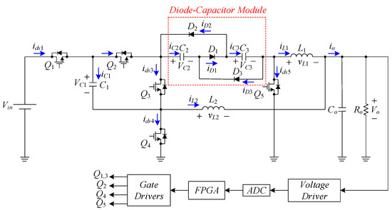
Figure 1.
Proposed interleaved high step-down converter.
Some symbols and definitions are to be given prior to dealing with this section, and are listed below:
- (1)
- The input voltage is signified by Vin and the output is denoted by Vo.
- (2)
- The values of the capacitors C1, C2, and C3 are large enough such that the voltages across them can be regarded as some constant values.
- (3)
- The currents in Q1, Q2, Q3, Q4, and Q5 are expressed by ids1, ids2, ids3, ids4, and ids5, respectively; the currents in C1, C2, and C3 are represented by iC1, iC2, and iC3, respectively; the currents in L1 and L2 are indicated by iL1 and iL2, respectively; the current iLo is the sum of iL1 and iL2; the currents in D1, D2, and D3 are signified by iD1, iD2, and iD3, respectively; the current Ro is expressed by Io.
- (4)
- The voltages on L1 and L2 are denoted by vL1 and vL2, respectively; the voltages on C1, C2, and C3 are expressed by VC1, VC2, and VC3, respectively; the voltage across Co is represented by Vo.
- (5)
- The switching period and frequency are indicated by Ts and fs, respectively.
- (6)
- The gate driving signals for Q1, Q2, Q3, Q4, and Q5 are denoted by vgs1, vgs2, vgs3, vgs4, and vgs5, respectively. Furthermore, vgs1 is in phase with vgs3 but is complimentary to vgs4, whereas vgs2 is complimentary to vgs5 and is shifted by 180o from vgs1. In addition, the duty cycle of vgs1 is Da, the duty cycle of vgs2 is Db and Da = Db = D.
- (7)
- Because the proposed circuit operates in the continuous conduction mode (CCM), there are four operating states over one switching period as shown in Figure 2.
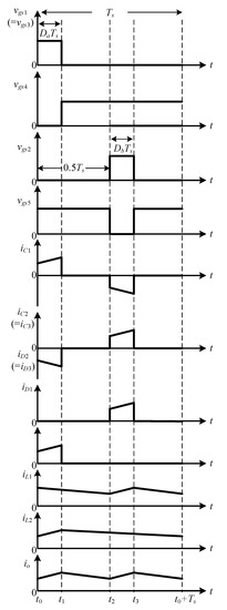 Figure 2. Illustrated key waveforms relevant to the proposed converter with Da = Db = D.
2.1. Basic Operating Principles
2.1.1. State 1:
As displayed in Figure 3, the switches Q1, Q3, and Q5 are turned on but the switches Q2 and Q4 are turned off, whereas the diode D1 is turned off but the diodes D2 and D3 are turned on. During this state, the input voltage Vin minus Vo is across the energy-transferring capacitor C1 and the inductor L2, thereby making C1 charged and L2 magnetized. At the same time, the energy-transferring capacitors C2 and C3 are discharged, and the inductor L1 is demagnetized due to the voltage across L1 being –Vo, thus rendering the current iL1 flow through the switch Q5.
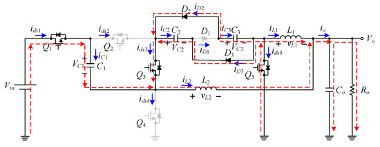
Figure 3.
Current flow of state 1.
2.1.2. States 2 and 4:
As displayed in Figure 4, the switches Q4, and Q5 are turned on but the switches Q1, Q2, and Q3 are turned off. During this state, the diodes D1, D2, and D3 are turned off. At the same time, the inductors L1 and L2 are demagnetized due to the voltages across L1 and L2 being −Vo, thereby rendering the currents iL1 and iL2 flow through the switches Q4 and Q5, respectively.
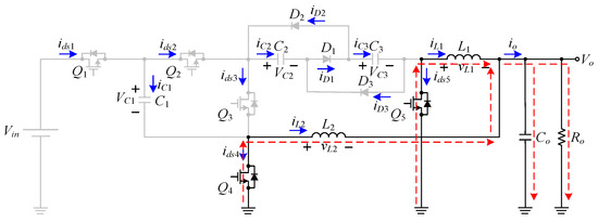
Figure 4.
Current flow of states 2 and 4.
2.1.3. State 3:
As displayed in Figure 5, the switches Q2 and Q4 are turned on but the switches Q1, Q3, and Q5 are turned off, whereas the diode D1 is turned on but the diodes D2 and D3 are tuned off. During this state, the energy stored in the energy-transferring capacitor C1 releases energy to the energy-transferring-capacitors C2 and C3, the inductor L1 and the load, thereby making C2 and C3 charged and L1 magnetized. At the same time, the inductor L2 is still demagnetized, thus making the current iL2 flow through the switch Q4. It is noted that the diode-capacitor module is composed of D1, D2, D3, C1, C2, and C3.
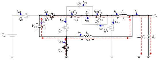
Figure 5.
Current flow of state 3.
2.2. Voltage Gain
By applying the voltage-second balance to the inductors L1 and L2, the following expressions can be obtained with Da = Db = D as
By substituting (3) and (4) into (1), the following expression can be found as
Finally, by substituting (5) into (2), the voltage gain can be obtained as
2.3. Boundary Conditions of L1 and L2
The condition of the boundary conduction mode (BCM) of the inductor L1 can be described as follows:
where IL1 and are the DC and AC values of the current iL1, respectively.
The condition of the BCM of the inductor L2 can be described as follows:
where IL2 and are the DC and AC values of the current iL2, respectively.
First of all, let two inductors be the same and three capacitors C1, C2, and C3 be identical. Accordingly, on the basis of the capacitor ampere-second balance of C1 and from states 1 and 3, the following expression can be obtained:
Since Da = Db = D, from (9), the relationship between IL1 and IL2 can be obtained as
According to Kirchiff’s current law, the following expression of DC value of iLo, called ILo, can be obtained as:
By substituting (10) into (11), the currents IL1 and IL2 can be represented as:
Also,
Therefore, by substituting (13) into (12), the following equations can be obtained as:
2.3.1. BCM Curve of L1
The ripple of the current flowing through the inductor L1, called , can be expressed by:
Therefore, as , the inductor L1 will operate in the CCM, namely,
where and Kcrit1(D) = 2(1 – D).
From (16), if , the inductor L1 works in the CCM; otherwise, the inductor L1 works in the DCM. Therefore, the boundary curve between the two modes can be drawn as shown in Figure 6.
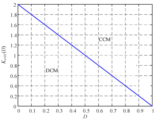
Figure 6.
Boundary curve between the two operating modes for the inductor L1.
2.3.2. BCM Curve of L2
The ripple of the current flowing through the inductor L2, called , can be indicated by
Therefore, as , the current L2 will operate in the CCM, namely,
where and .
From (18), if , the inductor L2 works in the CCM; otherwise, the inductor L2 works in the DCM. Therefore, the boundary curve between the two modes can be plotted as shown in Figure 7.
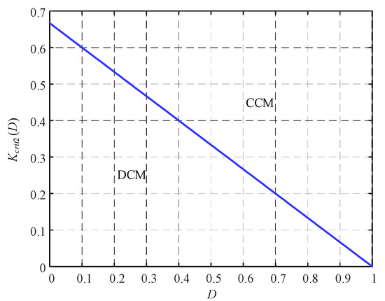
Figure 7.
Boundary curve between the two operating modes for the inductor L2.
2.4. Circuit Comparison
In this subsection, the proposed converter is compared with the existing circuits shown in [13,17,19,20] in terms of voltage gain, number of components, voltage stresses on switches and diodes, and floating output. The results are tabulated in Table 1.

Table 1.
Circuit comparison.
The proposed circuit has the same voltage gain as the circuits shown in [17,19], it has a lower voltage gain than the circuits shown in [13,20], it has a smaller component count than the circuits in [17,19], and it has a greater component count than the circuits in [13,20]. Furthermore, the proposed circuit and the circuit shown in [17] have no floating output. In addition, the average values of voltage stresses on switches and diodes for the circuits in [13,17,19,20], were 3/8Vin, 5/8Vin, 7/15Vin, and 11/32Vin, respectively. From this, it can be seen that the proposed has a smaller average value than the former two and a larger average value than the last two. In addition, for the proposed converter to be considered, the voltage across L1 is Vin – VC1 – Vo during the magnetizing period, whereas the voltage across L2 is VC1 – VC2 – VC3 during the magnetizing period. For the converter shown in [20] to be considered, the voltages across L1 and L2 are both 0.5Vin–Vo during the magnetizing period. Because the values of Vin – VC1 – Vo and VC1 – VC2 – VC3 are both smaller than 0.5Vin – Vo, the former has a lower voltage gain than the latter.
3. Design Considerations
Table 2 shows the system specifications. On the basis of this table, the associated components are designed.
Table 2.
System specifications.
3.1. Design of Inductors L1 and L2
From (16), if the inductor L1 works in the CCM, then the value of the inductor L1 should be satisfied with the following inequality:
where Ro,max is the load resistance at the minimum load. By substituting the system specifications shown in Table 1 and (19) into (20), the value range of the inductor L1 can be expressed as
From (18), if the inductor L2 works in the CCM, then the value of the inductor L2 should be satisfied with the following inequality:
By substituting the system specifications shown in Table 1 and (19) into (22), the value range of the inductor L2 can be expressed as
Finally, the values of L1 and L2 are identical and equal to 20 µH in order to meet the requirement of IL2 = 3IL1.
3.2. Design of Energy-Transferring Capacitors C1 to C3
As shown in state 1, the current waveform of the energy-transferring capacitor C1 is the same as that of the inductor L1, and hence the corresponding constant values can be expressed by
In addition, by assuming that the voltage ripple of C1 is 0.1% of VC1 and by substituting the results from (12), (19), and (25) into (26), the value of C1 can be obtained as
As shown in state 3, the current waveforms of the energy-transferring capacitors C2 and C3 are the same as that of the inductor L1, and hence the corresponding constant value can be represented by:
In addition, by assuming that the voltage ripples of C2 and C3 are both 0.1% of VC2, and by substituting the results from (12), (19), and (28) into (29), the values of C2 and C3 can be obtained as
Finally, in order to meet the assumption for (11), the values of C1, C2, and C3 are all set at 470 µF.
3.3. Design of Output Capacitor Co
The current flowing through the output capacitor Co is the sum of the currents iL1 and iL2, namely,
Because L1 = L2 = L, (30) can be rearranged as
After this, by assuming that the output voltage ripple of Co is 0.1% of Vo, and by substituting the results from Table 1, (19), and (31) into (32), the value of Co can be obtained to be
Eventually, the value of Co was chosen as 68 μF. In addition, Table 3 lists the component specifications of the proposed converter.
Table 3.
Component specifications.
4. System Control Strategy
Figure 8 shows the system configuration of the proposed interleaved high step-down converter, which is composed of the main power circuit and the feedback control circuit. As for the feedback control circuit, the output signal is extracted from the voltage divider. Afterwards, such an analog signal is sent to the analog-to-digital converter (ADC) and then is transferred to the digital signal. This digital signal is sent to the field programmable gate array (FPGA) so as to obtain the corresponding gate control signals. Finally, these control signals are used to drive the corresponding switches after individual gate drivers so as to keep the output voltage constant at some value.
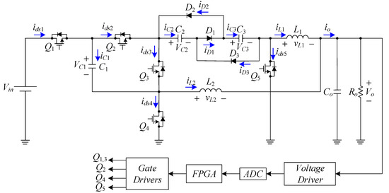
Figure 8.
System configuration for the proposed circuit.
5. Experimental Results
5.1. Measured Waveforms
Figure 9 shows the gate driving signals for the switches Q1, Q2, Q3, Q4, and Q5, called vgs1, vgs2, vgs3, vgs4, and vgs5, respectively. Figure 10 displays the voltages across Q1, Q2, Q4, and Q5, called vds1, vds2, vds4, and vds5. Figure 11 shows the voltages across Q1 and Q3, called vds1 and vds3. Figure 12 displays the voltages across the energy-transferring capacitors C1, C2, and C3, called VC1, VC2, and VC3, respectively. Figure 13 shows the voltages on the diodes D1, D2, and D3, called VD1, VD2, and VD3, respectively. Figure 14 displays the currents iL1, iL2, and iLo.
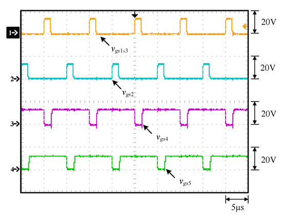
Figure 9.
Experimental waveforms at rated load: (1) vgs1,3, (2) vgs2, (3) vgs4, (4) vgs5.
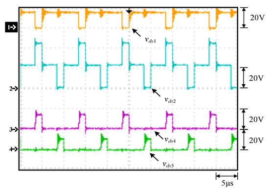
Figure 10.
Experimental waveforms at rated load: (1) vds1, (2) vds2, (3) vds4, (4) vds5.
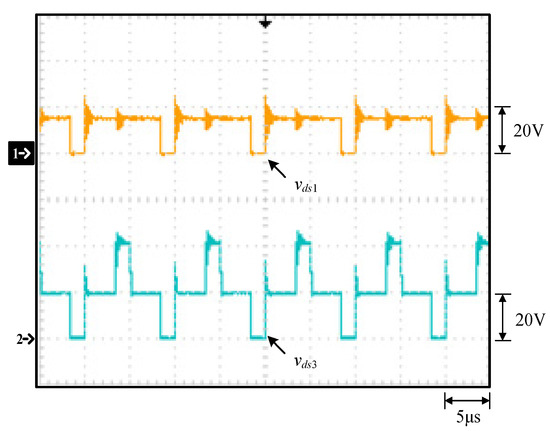
Figure 11.
Experimental waveforms at rated load: (1) vds1, (2) vds3.
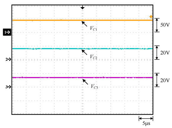
Figure 12.
Experimental waveforms at rated load: (1) VC1, (2) VC2, (3) VC3.
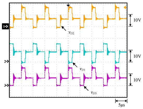
Figure 13.
Experimental waveforms at rated load: (1) vD2, (2) vD1, (3) vD3.
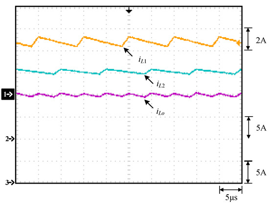
Figure 14.
Experimental waveforms at rated load: (1) iL1, (2) iL2, (3) iLo.
From Figure 9, it can be seen that the gate driving signal sequence met the requirements. From Figure 10 and Figure 11, it can be seen that the voltage stresses on Q1, Q4, and Q5, without voltage spikes considered, were all about 15 V, corresponding to Vin–VC1, whereas the voltage stresses on Q2 and Q3, without voltage spike considered, were about 45 V, corresponding to VC1. As for voltage spikes on switches during the turn-off period, they came from the resonance between line parasitic inductances and switch body capacitances. From Figure 12, it can be seen that the voltages across C1, C2, and C3 were kept at the values of 45.5 V, 15.5 V, and 15 V, respectively, which were slightly larger than the calculated values shown in Equations (25) and (28) at 45 V, 15 V, and 15 V, respectively. From Figure 13, it can be seen that the voltages across D1, D2, and D3 were three-level and the voltage stresses on these diodes were all about 15 V, corresponding to VC2. From Figure 14, it can be seen that the current iLo was the sum of the currents iL1 and iL2, whereas the DC values of iL1 and iL2 were about 5 A and 15 A, respectively, satisfying Equation (12).
5.2. Efficiency Measurement
The means of measuring the efficiency is given herein, and the accompanying result follows. As displayed in Figure 15, the input current was attained by measuring the voltage across the current sensing resistor according to the digital meter named Fluke 8050 A. Afterwards, the input voltage was also obtained by the digital meter. Hence, the input power can be obtained. Concerning the output power, the output current was read from the digital load and the output voltage was also attained by the digital meter. Hence, the output power can be obtained. Eventually, the resulting efficiency can be known. Accordingly, Figure 16 displays the curve of efficiency versus load current. From Figure 16, it can be known that the efficiency all over the load range was above 81.4% and the maximum efficiency was 85.1%.
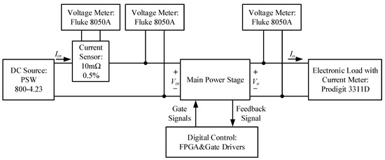
Figure 15.
Efficiency measurement block diagram.
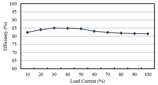
Figure 16.
Plot of efficiency versus load current.
5.3. Power Loss Breakdown Analysis
In the following section, the power loss breakdown analysis, not based on circuit modeling [21,22,23,24,25,26,27,28,29,30] but based on component datasheets, is shown under the condition that the converter operated at a rated load of 36 W.
5.3.1. Power Losses in Switches
The power loss in each switch, called PQ,loss, can be calculated on the basis of Equation (33).
where Pon,cond indicates the turn-on conduction loss, Pturn-on signifies the switching loss during the turn-on period, Pturn-off represents the switching loss during the turn-off period, Ron indicates the turn-on resistance, tr signifies the turn-on rising time, and tf represents the turn-off falling time. According to the FDP047AN datasheet, it can be known that the values of Ron, tr, and tf are 4 mΩ, 88 ns, and 45 ns, respectively.
Therefore,
Additionally, the total switch power loss, called PQ,loss,total, can be obtained from (34) to (38) as
5.3.2. Power Losses in Diodes
The power loss in each diode, called PD,loss, can be calculated on the basis of (40).
where VF signifies the forward bias voltage, and ID,avg represents the forward current.
In addition, the total diode power loss, called PD,loss,total, can be obtained from (41) to (43) as
5.3.3. Power Losses in Inductors
The power loss in each inductor, called PL,loss, can be calculated on the basis of (45).
where RDC signifies the copper resistance.
Additionally, the total inductor power loss, called PL,loss,total, can be obtained from (46) and (47) as
5.3.4. Estimated Efficiency
From Equations (39), (44), and (48), the power losses of components are drawn in Figure 17. In addition, the estimated efficiency was 83.8%, which is higher than the measured efficiency of 81.4%.
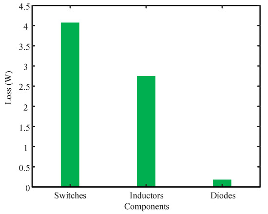
Figure 17.
Power losses of components.
6. Conclusions
An interleaved high step-down converter is presented herein. Compared with the related existing circuits [13,20] shown in Table 1, the proposed circuit had a relatively low step-down voltage gain under the same duty cycle, and had relatively low voltage stresses on the switches and diodes, thereby causing the switches with low turn-on resistances and the diodes with low forward bias voltages to be chosen. The main reason was that a diode-capacitor module utilized in the proposed converter can make inductors magnetized with relatively low voltages. Moreover, under the same voltage gain, the proposed circuit had a larger duty cycle than the circuits shown in [13,20], thereby rendering the elapsed time per cycle for the connection between the input and the output enlarged, and hence the controller not interrupted by noises.
Author Contributions
Conceptualization, K.-I.H.; methodology, K.-I.H.; software, J.-J.S.; validation, J.-J.S. and H.-H.T.; formal analysis, J.-J.S.; investigation, H.-H.T.; resources, K.-I.H.; data curation, H.-H.T.; writing—original draft preparation, K.-I.H.; writing—review and editing, K.-I.H.; visualization, H.-H.T.; supervision, K.-I.H.; project administration, K.-I.H.; funding acquisition, K.-I.H. All authors have read and agreed to the published version of the manuscript.
Funding
This research received no external funding.
Conflicts of Interest
The authors declare no conflict of interest.
References
- Ren, Y.; Xu, M.; Yao, K.; Lee, F.C. Two-stage 48V power pod exploration for 64-bit microprocessor. In Proceedings of the Eighteenth Annual IEEE Applied Power Electronics Conference and Exposition, Miami Beach, FL, USA, 9–13 February 2003; Volume 1, pp. 426–431. [Google Scholar]
- Ren, Y.; Xu, M.; Yao, K.; Meng, Y.; Lee, F.C. Two-stage approach for 12-V VR. IEEE Trans. Power Electron. 2004, 19, 1498–1506. [Google Scholar] [CrossRef]
- Mao, H.; Abu-Qahouq, J.A.; Luo, S.; Batarseh, I. Zero-voltage-switching (ZVS) two-stage approaches with output current sharing for 48V input dc-dc converter. In Proceedings of the Nineteenth Annual IEEE Applied Power Electronics Conference and Exposition, Anaheim, CA, USA, 22–26 February 2004; Volume 2, pp. 1078–1082. [Google Scholar]
- Ren, Y.; Xu, M.; Meng, Y.; Lee, F.C. 12V VR efficiency improvement based on two-stage approach and a novel gate driver. In Proceedings of the 2005 IEEE 36th Power Electronics Specialists Conference, Recife, Brazil, 16 June 2005; pp. 2635–2641. [Google Scholar]
- Fei, C.; Ahmed, M.H.; Lee, F.C.; Li, Q. Two-stage 48V-12V/6V-1.8V voltage regulator module with dynamic bus voltage control for light load efficiency improvement. IEEE Trans. Power Electron. 2017, 32, 5628–5636. [Google Scholar] [CrossRef]
- Xu, P.; Lee, F.C. Multiphase coupled-buck converter-novel high efficient 12 V voltage regulator module. IEEE Trans. Power Electron. 2003, 18, 74–84. [Google Scholar]
- Marvi, F.; Adib, E.; Farzanehfard, H. Interleaved zero voltage switching coupled inductor buck converter for low voltage-high current applications. In Proceedings of the 4th Annual International Power Electronics, Drive Systems and Technologies Conference, Tehran, Iran, 13–14 February 2013; pp. 236–241. [Google Scholar]
- Hwu, K.I.; Jiang, W.Z.; Wu, P.Y. An expandable two-phase interleaved ultrahigh step-down converter with automatic current balance. IEEE Trans. Power Electron. 2017, 32, 9223–9237. [Google Scholar] [CrossRef]
- Matsumoto, K.; Nishijima, K.; Sato, T.; Nabeshima, T. A two-phase high step down coupled-inductor converter for next generation low voltage CPU. In Proceedings of the 8th International Conference on Power Electronics-ECCE Asia, Jeju, Korea, 30 May–3 June 2011; pp. 2813–2818. [Google Scholar]
- Oraw, B.; Ayyanar, R. Small signal modeling and control design for new extended duty ratio, interleaved multiphase synchronous buck converter. In Proceedings of the INTELEC 06-Twenty-Eighth International Telecommunications Energy Conference, Providence, RI, USA, 10–14 September 2006; pp. 1–8. [Google Scholar]
- Esteki, M.; Poorali, B.; Adib, E.; Farzanehfard, H. Interleaved buck converter with continuous input current, extremely low output current ripple, low switching losses, and improved step-down conversion ratio. IEEE Trans. Ind. Electron. 2015, 62, 4769–4776. [Google Scholar] [CrossRef]
- Esteki, M.; Poorali, B.; Adib, E.; Farzanehfard, H. High step-down interleaved buck converter with low voltage stress. IET Power Electron. 2015, 8, 2352–2360. [Google Scholar] [CrossRef]
- Kirshenboim, O.; Peretz, M.M. High efficiency non-isolated converter with very-high step-down conversion ratio. IEEE Trans. Power Electron. 2017, 32, 3683–3690. [Google Scholar] [CrossRef]
- Nagaraja, H.N.; Patra, A.; Kastha, D. Design and analysis of four-phase synchronous buck converter for VRM applications. In Proceedings of the IEEE INDICON 2004. First India Annual Conference, Kharagpur, India, 20–22 December 2004; pp. 575–580. [Google Scholar]
- Lee, I.-O.; Cho, S.-Y.; Moon, G.-W. Interleaved buck converter having low switching losses and improved step-down conversion ratio. IEEE Trans. Power Electron. 2012, 27, 3664–3675. [Google Scholar] [CrossRef]
- Suja, A.; Sivakumar, S.; Ramkumar, P.S. Modified interleaved buck converter implementation for higher step-down conversion ratio. In Proceedings of the 2015 International Conference on Innovations in Information, Embedded and Communication Systems (ICIIECS), Coimbatore, India, 19–20 March 2015; pp. 1–4. [Google Scholar]
- Hwu, K.I.; Jiang, W.Z.; Wu, P.Y. An expandable four-phase interleaved high step-down converter with low switch voltage stress and automatic uniform current sharing. IEEE Trans. Ind. Electron. 2016, 63, 6064–6072. [Google Scholar] [CrossRef]
- Pan, C.-T.; Chuang, C.-F.; Chu, C.-C. A novel transformerless interleaved high step-down conversion ratio dc-dc converter with low switch voltage stress. IEEE Trans. Ind. Electron. 2014, 61, 5290–5299. [Google Scholar] [CrossRef]
- Chuang, C.-F.; Pan, C.-T.; Cheng, H.-C. A novel transformer-less interleaved four-phase step-down dc converter with low switch voltage stress and automatic uniform current-sharing characteristics. IEEE Trans. Power Electron. 2016, 31, 406–417. [Google Scholar] [CrossRef]
- Liao, S.-H.; Teng, J.-H.; Chen, S.-W. Bidirectional dc-dc converter with high step-down and step-up voltage gain. In Proceedings of the 2016 IEEE 2nd Annual Southern Power Electronics Conference (SPEC), Auckland, New Zealand, 5–8 December 2016; pp. 1–6. [Google Scholar]
- Ayachit, A.; Reatti, A.; Kazimierczuk, M.K. Magnetising inductance of multiple-output flyback dc-dc convertor for discontinuous-conduction mode. IET Power Electron. 2017, 10, 451–461. [Google Scholar] [CrossRef]
- Davoudi, A.; Jatskevich, J.; Chapman, P.L. Averaged modelling of switched-inductor cells considering conduction losses in discontinuous mode. IEEE Electron. Power Appl. 2007, 1, 402–406. [Google Scholar] [CrossRef]
- Kazimierczuk, M.K. Pulse-width Modulated dc-dc Power Converters, 2nd ed.; John Wiley & Sons: Hoboken, NJ, USA, 2015. [Google Scholar]
- Iftikhar, M.U.; Lefranc, P.; Sadarnac, D.; Karimi, C. Theoretical and experimental investigation of averaged modeling of non-ideal PWM DCDC converters operating in DCM. In Proceedings of the 2008 IEEE Power Electronics Specialists Conference, Rhodes, Greece, 15–19 June 2008; pp. 2257–2263. [Google Scholar]
- Nashed, M.; Fayed, A.A. A current-mode hysteretic buck converter with spur-free control for variable switching noise mitigation. IEEE Trans. Power Electron. 2018, 33, 650–664. [Google Scholar] [CrossRef]
- Davoudi, A.; Jatskevich, J.; Rybel, T.D. Numerical state-space average-value modeling of PWM DC-DC converters operating in DCM and CCM. IEEE Trans. Power Electron. 2006, 21, 1003–1012. [Google Scholar] [CrossRef]
- Amir, S.; Zee, R.V.D.; Nauta, B. An improved modeling and analysis technique for peak current-mode control-based boost converters. IEEE Trans. Power Electron. 2015, 30, 5309–5317. [Google Scholar] [CrossRef]
- Davoudi, A.; Jatskevich, J.; Chapman, P.L. Numerical dynamic characterization of peak current-mode-controlled DC-DC converters. IEEE Trans. Circuits Syst. II 2009, 56, 906–910. [Google Scholar] [CrossRef]
- Suntio, T. Average and small-signal modeling of self-oscillating flyback converter with applied switching delay. IEEE Trans. Power Electron. 2006, 21, 479–486. [Google Scholar] [CrossRef]
- Cheng, H.; Chen, C.J.; Wang, S.S. Small-signal model of flyback converter in continuous-conduction mode with peak-current control at variable switching frequency. IEEE Trans. Power Electron. 2018, 33, 4145–4156. [Google Scholar] [CrossRef]


© 2020 by the authors. Licensee MDPI, Basel, Switzerland. This article is an open access article distributed under the terms and conditions of the Creative Commons Attribution (CC BY) license (http://creativecommons.org/licenses/by/4.0/).