Abstract
In the last several years, thanks to the development and continuous improvement of semiconductor switching elements, and the simultaneous increase in interest in multi-phase drives, the investigation into constructing multi-phase converters has been growing. The matrix converter (MC) is considered to be one of the contenders for use in the multi-phase drive. In the context of using MC in the drive, it is expected to eliminate the common mode voltage (CMV). Another important problem is the ability to correct the input displacement angle to ensure the operation of the MC with unity input power factor. The purpose of the article is to present an MC modulation strategy that implements both CMV elimination and input displacement angle adjustment. Analytical and simulation analyses of the strategy, in application to three-to-multi-phase MC is presented. The suggested modulation strategy in applying to three-to-multi-phase MC is implemented in ATP-EMTP (Alternative Transients Program-ElectroMagnetic Transients Program) software. Simulation results are provided for a three-to-three-phase three-to-six-phase and three-to-nine-phase MC. The proposed modulation strategy is validated using an experimental approach.
1. Introduction
A matrix converter (MC) was invented and for the first time described in the early nineteen eighties by A. Alesina and M. Venturini [1,2] who analyzed the three-to-three-phase MC. The research in the area of MC has significantly accelerated since the publication of the first articles. Within three decades of publishing the first MC-related articles, many research centers around the world have been studying MC, focusing on, among other things, theoretical and practical implementation issues. In addition to the three-to-three-phase MC, new topologies have been proposed, such as indirect matrix converters (IMC) or multi-phase systems. Thanks to the development and continuous improvement of semiconductor switching elements, the interest in constructing multi-phase converters has been growing in the last several years. This is also associated with a simultaneous increase in interest in multi-phase drives.
One of the important problems in the application of not only the MCs, but also all converters controlled with use of pulse width modulation method, is the common mode current caused by the common mode voltage (CMV). Common mode voltage in a multi-phase drive is defined as a voltage between neutral point of the motor and the ground. Common mode currents introduce numerous problems. In aircrafts, for example, inductively coupled currents may interfere with other systems such as sensitive avionics equipment. In industrial applications, such current can cause malfunctions of computers and control equipment. In motor drives and electrical networks, common mode current even has the potential to cause physical damage to electric machines caused by bearing currents [3]. Reduction or better cancellation of CMV is really significant problem in the drive.
Many researchers have proposed methods to decrease the negative influence of the CMV on the drive and the supply network. Discussed in these papers, the methods focus on both hardware and software. The hardware solution, realized by adding a filter or auxiliary circuit, showed advantages such as low CMV, dv/dt, and EMI and overvoltage stress reduction [4,5,6,7]. The authors [6,7] present the entire elimination of the CMV in the MC with an integrated filter. However, hardware solutions result in increased size, weight, and cost of the converter, which are critical parameters in many applications. No extra cost is needed in the software approach. In the software solution, to achieve the CMV elimination, a modification of the modulation methods is applied. A majority of these methods are focused on modification of classic space vector modulation (SVM), applying active and zero voltage space vectors to synthesize output voltage in the MC [8,9,10,11,12,13,14]. The zero vectors resulting in the highest value of CMV are replaced by using combinations of active vectors or rotating space vectors, that are related to an increase in the number of switch commutations. Therefore, the authors of [8,10] analyze the influence of the proposed method on efficiency of the MC. The method based on modification of SVM achieves only partial reduction of the CMV. The method described in [10] reduces the peak value of the CMV by 42%, and in the paper [12], the CMV is reduced by 29% in peak value.
The only way to completely reduce the CMV in an MC is the use of rotating voltage space vectors for the synthesis of the output voltage in the MC. Elimination of the CMV in the MC by using rotating voltage space vectors has been investigated and presented by the authors of [15,16,17,18,19,20,21,22]. The authors of [17,18,19] present the SVM modulation method using only rotating input voltage space vectors. To determine the duty cycles, dq components of rotating space vector are discussed. Unfortunately, the method proposed in [17,18,19] involves a lot of computational effort.
To perform synthesis of output voltage with usage of the rotating voltage space vectors only, the authors of [20,23], in controlling of three-to-three-phase dual MC, have used a carrier based SVM method. The authors of [23,24] prove that in comparison with classic SVM, carrier based techniques can require less computation and result in simple implementation. Guided by this, the authors of the present article use the carrier based SVM method in the application of three-to-six-phase MC and of three-to-nine-phase MC. The total CMV elimination, in application to three-to-six-phase MC and to three-to-nine-phase MC, is presented in the author’s publication [25,26], but the modulation strategy proposed there has a drawback, that it cannot be used to control the phase shift angle of the current and voltage at the MC input. The present paper is focused on the presentation of the modulation strategy that eliminates this drawback and provides not only elimination of the CMV but also controlling the input displacement angle.
The ability to control the input displacement angle in the MC is an important problem in the context of cooperation with the power supply network. In general, a significant number of scientists, for example [27,28,29,30,31], are focused on developing an MC modulation method in which the input power factor is equal to one. The space vector modulation method is applied in these cases.
Elimination of CMV and adjustment of the input displacement angle in the three-to-multi-phase MC is a main goal of the proposed modulation method. The carrier based SVM method with usage of Venturini modulation functions is implemented. The application of the functions modulating the duty cycles for each of the MC switch separately allows arrangement of the conduction order of the MC switches during the switching period. The main goal of the proposed method is such arrangement of the switch duty cycles in switching period that provides not only rotating voltage space vectors for synthesizing the output voltages, but also implements the regulation of the MC input displacement angle. The discussed method was analyzed by the author of this article in relation to three-to-three-phase MC in [16,32,33,34]. The purpose of the present research is to extend it to use in MC with multiphase output. The presented modulation method is applicable to MCs that fulfill the condition, that the number of the output phases are the multiple of the input phases number. In turn, in the papers [35,36], it can be found that Venturini modulation method is feasible only for the MC, where the number of inputs is three. Taking into account these two conditions, the three-to-three-phase, three-to-six-phase and three-to-nine-phase MCs are analyzed in the present paper.
The disadvantage of the proposed method is that the small value of the voltage transfer ratio equals 0.5. The small value of voltage transfer ratio is inherently involved with the application of the Venturini modulation function used in the proposed modulation method. It should also be noted that the implementation of two set goals, i.e., CMV elimination and input displacement angle regulation, is associated with an increase in the number of commutations during the switching period. It may result in decreased efficiency of the MC. Contrarily, the proposed method does not increase the degree of input and output waveform distortions, which is important in the context of designing the filters necessary for the practical implementation of MC. Comparison of waveforms synthesized in the MC controlled using the proposed method with the classic use of the Venturini modulation function in relation to the three-to-three-phase MC was the subject of the author’s analysis in [32,37,38].
The article is organized as follows. In Section 2, the configuration and analytical model of the three-to-n-phase MC are introduced. Section 3 consists of a description of proposed modulation method as applied to three-to-three-phase, three-to-six-phase and three-to-nine-phase MC. The method of CMV elimination and the method of adjusting the input displacement angle are also presented in Section 3. Results of simulation and measurements are shown in the Section 4 and Section 5, respectively. The summary in Section 6 concludes the article.
2. Mathematical Description of the Three-to-n-Phase MC
The three-to-n-phase MC (Figure 1) being a direct frequency changer consists of a 3-phase voltage source at the input, and n-phase load at the output terminal, and 3n bidirectional fully controlled switches that can connect any output phase to any input phase. An operation of the switches related to output phase i and to input phase j is described by means of the switching function (1) [1].
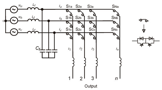
Figure 1.
The scheme of the 3-phase input n-phase output MC.
Taking into account voltage character of the input source and the inductive nature of the MC load, the switching functions for one of the output phases have to fulfill the following constraint: Sia + Sib + Sic = 1. The topology of the 3-phase input n-phase output may be considered in 3n different switching combinations.
The synthesized output voltage and input current waveforms are given by Equations (2) and (3), respectively, where: S is the matrix of the Sij switching functions; and are the input phase voltages; are the output phase voltages; ―the input phase currents; and are the output phase currents [1].
To find the switch duty cycles, the carrier based modulation is applied with application of the matrix: containing the Venturini modulation functions. The Equations (2) and (3) with usage of Venturini modulation functions are expressed as (4) and (5), respectively [1].
The Venturini modulation functions and for 3-phase input n-phase output MC used in the carrier based modulation are presented in the expressions (6)–(9). When these functions are used, the maximum value of voltage transfer ratio kU, defined in (9), is 0.5. Application of the modulation functions (6)–(9) allows to adjust the input displacement angle ϕi by changing the coefficients and .
In the proposed modulation method, CMV elimination occurs when the MC output voltages are synthesized using rotating voltage space vectors. Therefore, the definition of a space vector corresponding to multiphase voltage is quoted here. Instantaneous output voltage corresponding to individual combinations of the MC switching state, using Clark transformation (10), could be expressed as voltage space vectors. Output voltage space vectors may be divided into three groups: active voltage space vectors, zero voltage space vectors and rotating voltage space vectors. The number of these vectors, according to the number of switching state combinations in the three-to-multi-phase MC, is 3n.
3. Proposed Modulation Strategy
The carrier based approach is used in proposed modulation strategy. The separate modulation function is used to determine the switch duty cycles for each of the bidirectional switch. This allows setting the order of switch duty cycles in the Ts switching period. Thanks to this, the order of switch duty cycles in the period Ts are arranged so that the output voltages are synthesized by means of rotating voltage space vectors. This is, of course conditioned on the duty cycles being the same for the corresponding switches. The Venturini modulation functions (6)–(9) meet this requirement, and is shown in the next subsections of the article. The Venturini modulation functions (6)–(9) meet this requirement which, in respect to three-to-three-phase, three-to-six-phase and three-to-nine-phase MC, is shown in the next subsections of the article. Finding the same modulation function for the appropriate number of matrix switches is the first stage of implementation of the proposed methods for use in the selected MC system.
From the analyses carried out in the multi-phase MC [20], it follows that in order to achieve output voltage synthesized using only rotating voltage space vectors, the following conditions must be met:
- -
- At the same time, all input phase voltages should be used to synthesize the phase output voltages;
- -
- Simultaneously, each input phase must be connected to n/3 output phases;
The mentioned conclusions were drawn for the case when the voltages supplying the MC are the sinusoidal balanced voltage (11), and the CMV for three-to-n-phase MC is specified as (12). The Ui and ωi in the relation (11) are the amplitude and angular frequency, respectively. Taking into account the conclusions drawn from the [20], the proposed modulation strategy is addressed to the topology for which the number of output phases is an integer multiple of input phases number.
Regarding the possibility of the input displacement angle control, the following issues [21] are included:
- -
- If only the modulation functions (7) are used in modulation process, the input displacement angle is the same as the output one: ;
- -
- While the functions (8) are used to find the switching duty cycles, a phase shift between the input voltage and the input current fundamental component at the MC input terminals is: ;
- -
- To obtain the control of the input displacement angle, the modulation functions both and should be used in the switching period Ts.
The modulation strategy realizing both elimination of the CMV and control of the input displacement angle is presented in the Section 3.1, Section 3.2 and Section 3.3 for the examples of three-to-three-phase, three-to-six-phase and three-to-nine-phase MC, respectively.
3.1. Modulation Method Applied to Three-to-Three-Phase MC
After analyzing 27 possible switching state combinations related to three-to-three-phase MC, it can be noted that 6 of them correspond to rotating voltage space vectors. If the MC is supplied by balanced input voltage (11), the rotating voltage space vectors have the same modules, equal to the amplitude of the input voltage and have the same angular speed on the complex plane. Three of these vectors rotate in counter clockwise direction and are named CCW vectors, and rest of them rotate in clockwise direction and are named as CW vectors (Table 1).

Table 1.
The names and relationships defining the rotating voltage space vectors resulting in elimination of the CMV in three-to-three-phase MC.
Taking into account the expressions (4)–(9) in the application of three-to-three-phase MC, it should be seen that among nine modulation functions of the matrix, there are three three-element groups within which the modulation functions are equal to each other (13). The same observation can be made when considering the matrix (14). The matrix M has the form (15) and the phase output voltages (16). For each output phase, the sum of switch duty cycles must be equal to one, so the modulation functions for these switches must meet condition (17).
Taking into account the relations (13)–(15), three output phase voltages expressed by equations (16) can be represented within one Ts switching period by means of a space vector (18). As could be noted, the output voltage space vector is the sum of CCW rotating input voltage space vectors and CW rotating input voltage space vectors, mentioned in the Table 1. The application of these vectors to synthesize the output voltage results in elimination of the CMV could be easily checked. The duration of switching combinations corresponding to the input voltage space vectors are specified by the , , , , and switch duty cycles.
Application of both and matrices according to relationship (15) allows control of the input displacement angle by the change of the values of θ parameter, that is by the changing the and coefficients defined in (9).
Synthesis of the output voltage space vector according to Equation (18) is shown in Figure 2a. When applying carrier based modulation to realize proposed modulation strategy it should be assumed, that each Ts switching period is divided into two parts in proportion to values of and coefficients. Switch duty cycles, determined by means of modulation functions being the elements of and matrices, are arranged within Ts switching period in the sequence: , , , , , (Figure 2b). A block diagram of the implementation of the proposed modulation strategy, presenting signal flow for three switches connected to the output phase number 1, is shown in Figure 3.
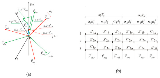
Figure 2.
Synthesis of output voltage during Ts switching period: (a) Summation of the input voltage rotating voltage space vectors; (b) switch duty cycles.
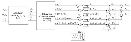
Figure 3.
Block diagram of the proposed modulation strategy for output phase number 1.
Results of the simulation and experimental tests, that confirm the presented considerations, are presented in the Section 4 of the paper.
The disadvantage of the method is that the small value of the voltage transfer ratio is equal to 0.5, which is inherently related to the use of the Venturini modulation functions in the form (6)–(9). The second drawback is the increased number of commutation in switching period Ts, compared to the classic Venturini modulation method. In the classic Venturini modulation method the switch duty cycles are determined by the use of sums of appropriate modulation functions and , and the matrix of the modulation functions has the form (19). The synthesis of the output voltage during Ts switching period is shown in the Figure 4.
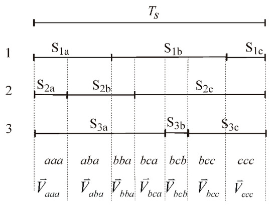
Figure 4.
Synthesis of output voltages during Ts switching period in classic Venturini modulation.
As could be seen in the Figure 2b and Figure 4, the proposed method is concerned with more switch commutation number in Ts switching period than the classic Venturini modulation method. It means that a lesser value of MC efficiency controlled is to be expected, with usage of proposed modulation method. Nevertheless, the classic Venturini modulation method results in the output voltage corresponding not only to rotating space vectors (), but also to active (, , , ) and zero vectors (, ), and so does not realize the CMV elimination.
3.2. Modulation Method Applied to Three-to-Six-Phase MC
The proposed modulation strategy in the application of the three-to-six-phase MC is realized by applying the Venturini modulation functions, presented as Equations (20)–(22). The usage of the modulation functions (20), that depend on the difference between the output frequency and input frequency, causes the input displacement angle to be the same as the output one: . It could be noticed, that there are six groups for three of the modulation functions in which the same function defines the duty cycles for three switches. The analogous groups are found in the matrix (21), where modulation functions depend on the sum of input and output angular frequency and the application of the results in . The usage of both of matrices and according to the Equation (22) allows to control the input displacement angle in the range . Elimination of the CMV is obtained by suitable arrangement of the switch duty cycles in the Ts switching period. As it was said in Section 3.1, the elimination of CMV is obtained when the output voltage is synthesized with usage of rotating input voltage space vectors. As could be seen, the output voltage space vector (23) depends on CCW and CW rotating voltage space vectors, representing three phase input voltages (Table 1), the application of which results in elimination of the CMV.
The block diagram of the proposed carrier based modulation realizing voltage at the output phase number “1” is almost the same as in Figure 3, with the difference that the modulation functions (20) and (21) are taken instead of the functions (13) and (14). The switch duty cycles arrangement, resulting in elimination of the CMV, for the switching period Ts and for the six output phases is shown in Figure 5. It could be noted in Figure 4 that the output voltages of three of six phases: 1, 3 and 5 or 2, 4 and 6 correspond to appropriate rotating space vectors , , and , , . Taking into account six output phases, the voltages of these phases correspond to vectors recorded as: . The letters in the label xxxxxx in the name of the space vector means the names of input phases connected into output phase 1, 2, 3, 4, 5 and 6, respectively. The vectors representing output voltages of all three-to-six-phase MC configurations which realize elimination of the CMV are shown in Table 2. The voltage space vectors, presented in Table 2, are divided in three groups. Two of them consist of the CCW and CW rotating voltage space vectors, that are characterized by the same module value equal 0.866Ui. The third group in Table 2 are zero vectors whose module is equal to zero [25].
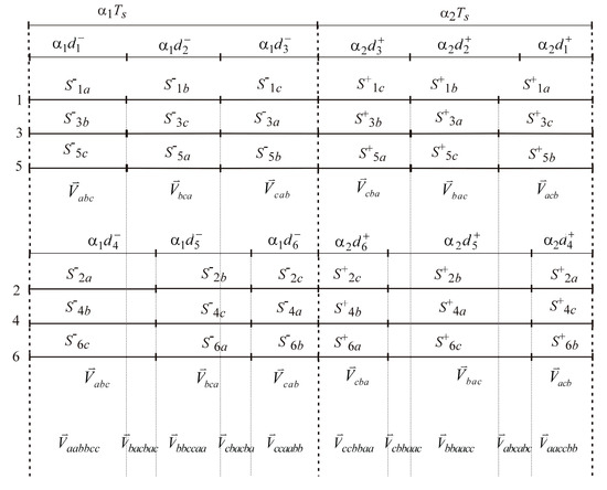
Figure 5.
Switch duty cycles during Ts switching period in three-to-six-phase MC for output phase numbers 1, 3 and 5; numbers 2, 4, and 6.
Table 2.
The names and relationships defining the rotating and zero voltage space vectors resulting in elimination of the CMV in three-to-six-phase MC.
3.3. Modulation Method Applied to Three-to-Nine-Phase MC
Similarly to the modulation functions discussed previously in the Section 3.1 and Section 3.2, Venturini modulation functions (24) and (25) applied to control the three-to-nine-phase MC, have the property that they are the same for three of nine switches. This allows the arrangement of switch duty cycles to be used in the Ts period in a manner analogous to those considered in application to the three-to-three-phase and three-to-six-phase MC (Figure 6). The Ts switching period is divided into two parts depending on values of and parameters, which define the referenced input displacement angle. The application of the proposed arrangement of switch duty cycles is consistent with the relationship (26).
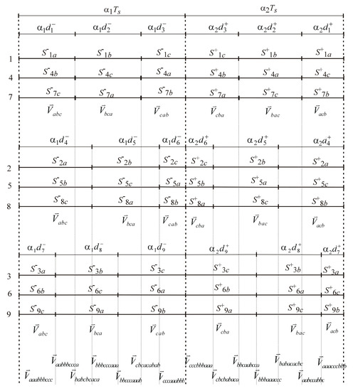
Figure 6.
Switch duty cycles during Ts switching period in three-to-nine-phase MC for output phase numbers 1, 4 and 7; numbers 2, 5, and 8; numbers 3, 6, and 9.
The output voltage space vector (27), averaged in Ts period, depends on input voltage rotating space vectors , , and , , (Table 1), resulting in zero value of CMV. The rotating voltage space vectors in Figure 6 represent the nine output phase voltages, and the letters in the label xxxxxxxxx denote the names of input phases connected to the output phases numbered as 1, 2, 3, 4, 5, 6, 7, 8, 9, respectively. All the admissible vectors which are synthesized by usage of modulation functions (24) and (25) can be seen in Table 3. Rotating voltage space vectors representing nine-phase output voltage of MC are characterized by three different module values. Half of the presented vectors are the CCW vectors and rest of them are the CW type vectors. Applying both of them in the way presented in Figure 6 allows the controlling of the input displacement angle.
Table 3.
Rotating voltage space vectors leading to elimination the CMV in three-to-nine-phase MC.
4. Simulation Analysis
According to the presented mathematical analysis of the proposed modulation strategies, three-to-three-phase, three-to-six-phase and three-to-nine-phase MC simulation models have been developed. The ATP-EMTP software have been used. To model the MC bidirectional switches, the ideal TACS-controlled TYPE 13 switches are used. Ideal balanced sinusoidal voltage sources are applied as supplying voltages and resistive-inductive elements as an n-phase load. Logical equations describing the modulation strategy are modelled in the TACS cards TYPE 98.
The controlling switch signals are worked out for the defined values of parameters that describe the power circuit, and for the referenced values that determine the desired input displacement angle, voltage transfer ratio, output displacement angle, and output frequency (Table 4). The example of the three-to-three-phase MC simulation model is shown in Figure 7.
Table 4.
The parameters used in simulations.
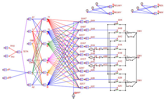
Figure 7.
Simulation model of three-to-three-phase MC controlled with usage of the proposed modulation method.
The simulation results regarding the problem of CMV elimination in the considered MCs are shown in Figure 8. The waveforms of output phase voltage and waveforms of CMV are shown in the parts (a), (c) and (e) of the mentioned figure for three-to-three-phase MC, for three-to-six-phase MC, for three-to-nine-phase MC, respectively. The instantaneous values of phase output voltages are equal to the instantaneous values of the input phase voltages. As can be seen, the CMV received in simulation tests equals zero in each of three-to-n-phase MC. The zero value of CMV results from the fact that the output voltage is synthesized by usage of rotating voltage space vectors, seen in parts (b), (d) and (f) of Figure 8, where the space vector trajectories are circular. The three-to-three-phase MC (Figure 8b) may be seen switching between only rotating space vectors having the same modules equal the amplitude Ui of input phase voltage. Rotating space vectors with two values of the modules are used to synthesize the output voltage in three-to-six-phase MC: First value, equal to 0.865 of the input phase voltage amplitude Ui and; second value, equal to zero value, seen in Figure 8d. The trajectory of the output voltage space vectors in three-to-nine-phase MC (Figure 8e) is shaped by the rotating space vectors having three different values of the modules: 0.2993Ui; 0.449Ui and 0.844Ui.
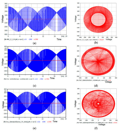
Figure 8.
Output phase voltage (blue) and CMV (red) for: three-to-three-phase MC (a); three-to-six-phase MC (c); three-to-nine-phase MC (e). Trajectory of the output voltage for: three-to-three-phase MC (b); three-to-six-phase MC (d); three-to-nine-phase MC (f).
The results of simulations involved in testing the possibility to control the input displacement angle are shown in Figure 9: for three-to-three-phase MC (Figure 9a,b); for three-to-six-phase MC (Figure 9c,d); and for the three-to-nine-phase MC (Figure 9e,f). In the parts (a), (c) and (e) of Figure 9, the input phase voltages and input MC currents are shown. The parts (b), (d) and (f) of Figure 9 depict the input displacement angle versus referenced input displacement angle. The values of the displacement angle are determined between input voltage and fundamental component of the current. As could be noticed in each of the three figures, implementation of the Venturini modulation functions into modulation method causes the dependence of the input displacement angle on the referenced value of this angle to have a shape approximately corresponding to the function tangent, which is consistent with the analytical description of the modulation method. A positive value of the input displacement angle means that the fundamental harmonic of input current is lagging. For a negative value of this angle, the fundamental harmonic of input current has leading nature.
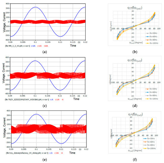
Figure 9.
Input phase voltage (blue) and input current (red) for: three-to-three-phase MC (a); three-to-six-phase MC (c) and three-to-nine-phase MC (e). Input displacement angle versus referenced input displacement angle for: three-to-three-phase MC (b); three-to-six-phase MC (d); three-to-nine-phase MC (f).
5. Experimental Measurements
The measurements were carried out on the laboratory model of three-to-three-phase matrix converter system, the diagram can be divided into three main parts (Figure 10a): The power circuit, the control, and the modulation. The power circuit of the matrix converter consists of a matrix of nine bidirectional MC switches, an input filter Fi, and an overvoltage protection circuit PP. In the MC matrix (Figure 10b), three switches realizing connection of one of the three output phases with three input phases are grouped in a single integrated circuit EPM 25-D 00112, which is a modification of BSM 25 GD 120 DN2 circuit manufactured by Siemens, made by order of Danfoss-Drives A/S. The PWM control realizes synthesis of required output voltage and input current waveforms, together with setting the phase shift between first harmonic of input current and respective input voltage. At the design stage, the necessity to examine various PWM methods was anticipated, therefore the PWM signals were software-generated and transmitted to the control system by means of the PCL–1800 I/O board. The proper commutation process, ensuring fulfillment of fundamental requirement concerning avoidance of shortening voltage sources, or input phases, and currents sources, or inductance-type load phases, is realized in the electronic part of the control in the form of four-step commutation with load phase currents direction control. In Table 5, values of parameters used in the measurement test are shown.
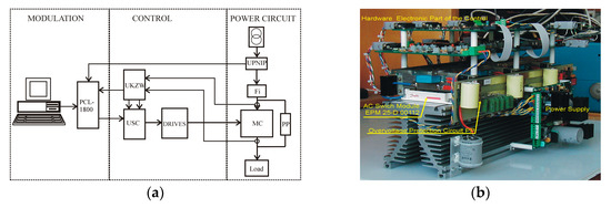
Figure 10.
Laboratory model of MC: (a) Diagram system; (b) power and control system.
Table 5.
The parameters used in laboratory measurements.
In Figure 11, the chosen waveforms of input and output voltage and currents are shown. The waveforms are registered for voltage transfer ratio kU = 0.5, output frequency fo = 60 Hz, and input displacement angle . The waveforms correspond to the results of simulation tests. Particular attention should be paid to the waveform of CMV (Figure 11c), because an elimination of the CMV was the main goal of the proposed modulation method.
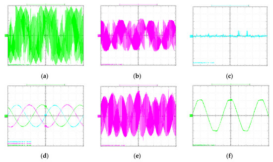
Figure 11.
Waveforms registered in three-to-three-phase MC: output line-line voltage (a); output phase voltage (b); CMV (c); output currents (d); input current (e); input phase voltage (f).
To establish the dependence of input displacement angle on the referenced value of this angle, the simulation characteristics are compared in Figure 12. These characteristics, prepared for different values of output frequency, show close convergence.
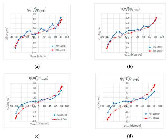
Figure 12.
Input displacement angle in the function of referenced input displacement angles for different values of output frequency in three-to-nine-phase MC: Results of simulation (red line); result of measurements (blue line). (a): fo = 50 Hz; (b): fo = 60 Hz; (c): fo = 80 Hz; (d): fo = 100 Hz.
6. Discussion
The article presents a modulation method that allows both CMV elimination and input angle control in three-to-n-phase MC. Entire elimination of the CMV in MC is possible when only the rotating voltage space vectors are used in synthesizing the output voltages. In classic modulation methods applied to control of the MC, the usage of only active and zero space vectors is assumed. Application of rotating voltage space vectors in space vector modulation is cumbersome due to their time-varying position on the complex plane. In the proposed modulation method, application of rotating space vectors is realized by the carrier based modulation with usage of Venturini modulation functions. Accomplishment of the assumed goal, i.e., synthesis of output voltage with application only of the rotating voltage space vectors, required the correct setting of the switch duty cycles within the switching period, which is realized in the proposed method.
The usage of Venturini modulation function to realize the elimination of CMV in the three-to-three-phase and three-to-six-phase MC was discussed in previous works of the author. However, CMV elimination with simultaneous input angle control was only analyzed for three-to-three-phase MC. Realization of both goals, concerning the three-to-six-phase MC and the three-to-nine-phase MC, were not presented in the publications. Elimination of the CMV and controlling of the input displacement angle in three-to-n-phase MC are the important problems in the context of the multi-phase drives development and compatibility of them with the supplying network.
The disadvantage of the proposed method, which should be analyzed in a further research, is that the decreased value of MC efficiency resulted in an increased number of commutation in the switching period. A low value of the voltage transfer ratio (kU = 0.5) is also a disadvantage of the proposed modulation method. Future research could be focused on implementation of the proposed modulation method into dual multi-phase MC that allow to receive the voltage transfer ratio kU equal to one or even 1.5.
Funding
This research received no external funding.
Conflicts of Interest
The authors declare no conflict of interest.
References
- Venturini, M.; Alesina, A. The generalized transformer: A new bidirectional, sinusoidal waveform frequency converter with continuously adjustable input power factor. In Proceedings of the IEEE Power Electronics Specialists Conference, Atlanta, GA, USA, 16–20 June 1980; pp. 242–252. [Google Scholar] [CrossRef]
- Alesina, A.; Venturini, M.G.B. Analysis and design of optimum-amplitude nine-switch direct AC-AC converters. IEEE Trans. Power Electron. 1989, 4, 101–112. [Google Scholar] [CrossRef]
- Julian, A.L.; Oriti, G.; Lipo, T.A. Elimination of common-mode voltage in three-phase sinusoidal power converters. IEEE Trans. Power Electron. 1999, 14, 982–989. [Google Scholar] [CrossRef]
- Ogasawara, S.; Ayano, H.; Akagi, H. An active circuit for cancellation of common-mode voltage generated by a PWM inverter. IEEE Trans. Power Electron. 1998, 13, 835–841. [Google Scholar] [CrossRef]
- Akagi, H.; Tamura, S. A passive EMI filter for eliminating both bearing current and ground leakage current from an inverter-driven motor. IEEE Trans. Power Electron. 2006, 21, 1459–1469. [Google Scholar] [CrossRef]
- Yamada, K.; Higuchi, T.; Yamamoto, E.; Hara, H.; Sawa, T.; Swamy, M.M.; Kume, T. Filtering Techniques for Matrix Converters to Achieve Environmentally Harmonious Drives. In Proceedings of the 2005 European Conference on Power Electronics and Applications, Dresden, Germany, 11–14 September 2005; p. 10. [Google Scholar] [CrossRef]
- Kume, T.; Yamada, K.; Higuchi, T.; Yamamoto, E.; Hara, H.; Sawa, T.; Swamy, M.M. Integrated Filters and Their Combined Effects in Matrix Converter. IEEE Trans. Ind. Appl. 2007, 43, 571–581. [Google Scholar] [CrossRef]
- Espina, J.; Arias, A.; Balcells, J.; Ortega, C. Common Mode Output Waveforms Reduction for Matrix Converters Drives. In Proceedings of the 2009 35th Annual Conference of IEEE Industrial Electronics, Porto, Portugal, 3–5 November 2009; pp. 4499–4504. [Google Scholar] [CrossRef]
- Padhee, V.; Sahoo, A.K.; Mohan, N. Modulation technique for common mode voltage reduction in a matrix converter drive operating with high voltage transfer ratio. In Proceedings of the 2016 IEEE Applied Power Electronics Coference and Exposition (APEC), Long Beach, CA, USA, 20–24 March 2016; pp. 1982–1988. [Google Scholar] [CrossRef]
- Nguyen, H.-N.; Lee, H.-H. A DSVM Method for Matrix Converters to Suppress Common-mode Voltage with Reduced Switching Losses. IEEE Trans. Power Electron. 2016, 31, 4020–4030. [Google Scholar] [CrossRef]
- Padhee, V.; Sahoo, A.K.; Mohan, N. Modulation Techniques for Enhanced Reduction in Common-Mode Voltage and Output Voltage Distortion in Indirect Matrix Converters. IEEE Trans. Power Electron. 2017, 32, 8655–8670. [Google Scholar] [CrossRef]
- Guan, Q.; Wheeler, P.W.; Guan, Q.; Yang, P. Common-Mode Voltage Reduction for Matrix Converters Using All Valid Switch States. IEEE Trans. Power Electron. 2016, 31, 8247–8259. [Google Scholar] [CrossRef]
- Rahman, K.; Iqbal, A.; Al-Emadi, N.; Ben-Brahim, L. Common mode voltage reduction in a three-to-five phase matrix converter fed induction motor drive. IET 2017, 10, 817–825. [Google Scholar] [CrossRef]
- Ahmed, S.M.; Salam, Z.; Abu-Rub, H. Common-Mode Voltage Elimination in a Three-to-Seven Phase Dual Matrix Converter Feeding A Seven Phase Open-End Induction Motor Drive. In Proceedings of the 2014 IEEE Conference on Energy Conversion (CENCON), Johor Bahru, Malaysia, 13–14 October 2014; pp. 207–212. [Google Scholar] [CrossRef]
- Milanovic, M.; Dobaj, B. A Novel Unity Power Factor Correction Principle in Direct AC to AC Matrix Converters. In Proceedings of the PESC’98, IEEE Power Electronics Specialists Conference, Fukuoka, Japan, 17–22 May 1998; pp. 746–752. [Google Scholar] [CrossRef]
- Rząsa, J. Control of a Matrix Converter with Reduction of a Common Mode Voltage. In Proceedings of the IEEE Compatibility in Power Electronics, “CPE20015”, Gdańsk-Sobieszewo, Poland, 1–3 June 2005; pp. 213–217. [Google Scholar]
- Nguyen, H.; Nguyen, T.D.; Lee, H. A Modulation Strategy to Eliminate CMV for Matrix Converters with Input Power Factor Compensation. In Proceedings of the IECON 2016―42nd Annual Conference of the IEEE Industrial Electronics Society, Florence, Italy, 23–26 October 2016; pp. 6237–6242. [Google Scholar] [CrossRef]
- Nguyen, H.; Lee, H. A Modulation Scheme for Matrix Converters with Perfect Zero Common-Mode Voltage. IEEE Trans. Power Electron. 2016, 31, 5411–5422. [Google Scholar] [CrossRef]
- Nguyen, H.N.; Nguyen, T.D.; Lee, H.H. Development of generalized relationship between active and rotating vectors in matrix converter. Electron. Lett. 2019, 55, 339–341. [Google Scholar] [CrossRef]
- Mohapatra, K.K.; Mohan, N. Open-End Winding Induction Motor Driven with Matrix Converter for Common-Mode Elimination. In Proceedings of the International Conference on Power Electronics, Drives and Energy Systems, New Delhi, India, 12–15 December 2006. [Google Scholar]
- Rząsa, J. Research on Dual Matrix Converter Feeding an Open-End-Winding Load Controlled with the Use of Rotating Space Vectors. Part, I. In Proceedings of the IEEE IECON, Vienna, Austria, 10–13 November 2013; pp. 4919–4924. [Google Scholar]
- Rząsa, J.; Garus, G. Research on Dual Matrix Converter Feeding an Open-End-Winding Load Controlled with the Use of Rotating Space Vectors. Part II. In Proceedings of the IEEE IECON, Vienna, Austria, 10–13 November 2013; pp. 4925–4930. [Google Scholar]
- Baranwal, R.; Basu, K.; Mohan, N. Carrier-Based Implementation of SVPWM for Dual Two-Level VSI and Dual Matrix Converter with Zero Common-Mode Voltage. IEEE Trans. Power Electron. 2015, 30, 1471–1487. [Google Scholar] [CrossRef]
- Baranwal, R.; Basu, K.; Mohan, N. An Alternative Carrier based implementation of Space Vector PWM for Dual Matrix Converter Drive with Common Mode Voltage Elimination. In Proceedings of the IEEE IECON, Dallas, TX, USA, 29 October–1 November 2014. [Google Scholar]
- Rząsa, J.; Sztajmec, E. Elimination of Common Mode Voltage in Three-To-Six-Phase Matrix Converter. Energies 2019, 12, 1662. [Google Scholar] [CrossRef]
- Rząsa, J.; Sztajmec, E. Elimination of Common Mode Voltage in Three-To-Nine-Phase Matrix Converter. Energies 2020, 13, 631. [Google Scholar]
- Wheeler, P.W.; Rodriguez, J.; Clare, J.C.; Empringham, L.; Weinstein, A. Matrix converters: a technology review. IEEE Trans. Ind. Electron. 2002, 49, 276–288. [Google Scholar] [CrossRef]
- Rodriguez, J.; Rivera, M.; Kolar, J.W.; Wheeler, P.W. A Review of Control and Modulation Methods for Matrix Converters. IEEE Trans. Ind. Electron. 2012, 59, 58–70. [Google Scholar] [CrossRef]
- Casadei, D.; Grandi, G.; Serra, G.; Tani, A. Space Vector Control of Matrix Converters with Unity Input Power Factor and Sinusoidal Input/Output Waveforms. In Proceedings of the 1993 Fifth European Conference on Power Electronics and Applications, Brighton, UK, 13–16 September 1993. [Google Scholar]
- Huber, L.; Borojevic, D. Space vector modulated three-phase to three-phase matrix converter with input factor correction. IEEE Trans. Ind. Appl. 1995, 31, 1234–1246. [Google Scholar] [CrossRef]
- Niang, T.; Hui, H.; Chao, S. Novel Algorithm of Matrix Converter with Indirect Space Vector Modulation. In Proceedings of the 2018 International Conference on Power System Technology (POWERCON), Guangzhou, China, 6–8 November 2018; pp. 4910–4917. [Google Scholar]
- Rząsa, J. Selected Methods of Input Current and Output Voltage Waveforms in Matrix Converters. Ph.D. Thesis, Warsaw University of Technology, Warsaw, Poland, 2001. (In Polish). [Google Scholar]
- Rząsa, J. Influence of Control Strategy in Classic Venturini Modulation Method on Synthesized Output Voltages and Input Currents of Matrix Converter. Arch. Electr. Eng. 2005, 54, 229–251. [Google Scholar]
- Rząsa, J. Vector Interpretation of the Control According to the Venturini Method in a Matrix Converter. In Proceedings of the Komputerowe Systemy Wspomagania Nauki, Przemysłu i Transportu “TRANSCOMP”, Zakopane, Poland, 3–6 December 2012. (In Polish). [Google Scholar]
- Ali, M.; Iqbal, A.; Khan, M.R.; Ayyub, M.; Anees, M.A. Generalized Theory and Analysis of Scalar Modulation Techniques for a m × n Matrix Converter. IEEE Trans. Power Electron. 2017, 32, 4864–4877. [Google Scholar] [CrossRef]
- Ali, M.; Iqbal, A.; Anees, M.A.; Khan, M.R.; Rahman, K.; Ayyub, M. Differential evolution-based pulse-width modulation technique for multiphase MC. IET Power Electron. 2019, 12, 2224–2235. [Google Scholar] [CrossRef]
- Rząsa, J. Relationships between Input and Output Current in the Matrix Converter (MC). In Proceedings of the 3rd International Workshop Compatibility in Power Electronics “CPE 2003”, Gdańsk-Sobieszewo, Poland, 28–30 May 2003; pp. 121–123. [Google Scholar]
- Rząsa, J. Low-Frequency Components in the Switch Currents of Matrix Converter. In Proceedings of the 2011 IEEE International Symposium on Industrial Electronics, Gdansk, Poland, 27–30 June 2011; pp. 323–328. [Google Scholar] [CrossRef]


© 2020 by the author. Licensee MDPI, Basel, Switzerland. This article is an open access article distributed under the terms and conditions of the Creative Commons Attribution (CC BY) license (http://creativecommons.org/licenses/by/4.0/).