Abstract
In this paper, we present the results of a preliminary study on the self-powered autonomous wireless sensor node by using thermoelectric energy generator based on Silicon (Si) thermoelectric legs, energy management integrated circuit (EMIC), Radio Frequency (RF) module with a temperature and humidity sensor, etc. A novel thermoelectric module structure is designed as an energy generator module, which consists of 127 pairs of Silicon legs and this module is fabricated and tested to demonstrate the feasibility of generating electrical power under the temperature gradient of 70K. EMIC has three key features besides high efficiency, which are maximum power point tracking (MPPT), cold start, and complete self-power operation. EMIC achieved a cold start voltage of 200 mV, peak efficiency of 78.7%, MPPT efficiency 99.4%, and an output power of 34 mW through only the Thermoelectric Generator (TEG) source. To assess the capability of the device as a small scale power source for internet of things (IoT) service, we also tested energy conversion and storage experiments. Finally, the proposed sensor node system which can transmit and monitor the information from the temperature and humidity sensor through the RF module in real time demonstrates the feasibility for variable applications.
1. Introduction
With the recent progress of mobile technologies and remote sensing systems, internet of things (IoT) has been of great interest due to their potential to create a large market and their significant impact on human life [1,2,3,4]. In realizing various IoT services, one of the main problems yet to be solved is the finite power capacity of batteries in sensor nodes. Fixed energy sources, such as batteries and fuel cells, are bulky with a finite amount of energy and have serious disadvantages such as limited lifetime, periodic recharging or replacement, and use of hazardous chemicals. Therefore, many researchers have been studied the scavenging energy from the environment. There are several power-generating methods using ambient environmental energy including thermal gradients, solar energy, triboelectric energy and vibration energy [5,6,7,8,9,10,11,12,13]. Among them, driving a thermoelectric generator from wasted heat is advantageous in that it can use a variety of heat sources such as automobiles, power plants, ships, and humans without time constraints unlike sunlight. In addition, the thermoelectric energy has attracted a great deal of attention because of its DC power, sustainability of the power source, and controllability of the output voltage, etc. Especially at the point of DC, for example, a piezoelectric or electromagnetic, AC type energy conversion device requires a rectifier to convert AC to DC, as a result the energy efficiency is reduced by the losses in the rectifier. Conversion of environmental heat to electrical energy has been actively studied using a variety of thermoelectric materials, and in particular there have been many attempts to apply various materials [14,15,16,17,18,19] to thermoelectric generator recently.
Section 2 shows thermoelectric device, the proposed energy management integrated circuit (EMIC) and Wireless Sensor Network (WSN) system design issues, Section 3 presents the structure and fabrication of silicon thermoelectric devices and modules, and Section 4 shows the structure, function, and performance of the proposed EMIC. Section 5 presents wireless sensor node system applicable to the IoT applications through the proposed silicon device and EMIC, and Section 6 provides some concluding remarks.
2. Device and System Design Issues
2.1. Thermoelectric Device Design Issues
In this study, for easy mass production, low cost, and rare harmfulness, we report on the performance of thermoelectric generator module based hetero-structured Si legs, energy management integrated circuit (EMIC), and a wireless sensor node system with RF module and temperature and humidity sensor. In silicon thermoelectric devices, studies [20,21,22] for improving the performance of individual devices have been actively conducted. However, the research on modularization, packaging, and application to actual WSN system is still insufficient. In order to extract the energy of the available level, it is important to perform optimal modularization and packaging for high performance as well as to improve the performance of individual devices. For this purpose, a thermoelectric device bridge of heterostructure was fabricated by using silicon wafer thermoelectric material, and the Seebeck coefficient was measured using a self-made system. In addition, a hybrid cu paste was used to connect the thermoelectric elements to the upper and lower substrates to fabricate the module, and the thermoelectric power of the module was measured.
2.2. Proposed EMIC and WSN System Design Issues
Next, to the thermoelectric EMIC suitable for the WSN, it is necessary to extract the power from the thermoelectric module as much as possible, maintain the operation without being affected by the surrounding environment and minimize the loss, transfer energy with high efficiency. That is, EMIC requires the following features: maximum power point tracking (MPPT), cold start, and high efficiency. LTC’s 3108 [23], which is widely used as a commercial product, can start at very low voltage (20 mV) in low temperature difference environment, but it has no MPPT function and low efficiency. TI’s 25504 [24] has the advantage of high efficiency (over 80%), but it has the disadvantage that the MPPT function is limited and the cold start voltage is higher than about 600 mV. The EMIC proposed in this study is designed to include all the advantages of the above two products.
In addition, the EMIC must be operated using only the Thermoelectric Generator (TEG) power source, and all external sources (reference voltage and clock) must be removed. However, in the previous research [25,26,27], it was not possible to generate low and stable reference voltages during start-up mode operation and low power, adaptive clock signals for the boost mode operation. So they were supplied from outside. In this study, we added adjustable clock signals with low power consumption, and stable reference voltages generated from a low supply voltage, which allows it to work perfectly with TEG alone.
Finally, wireless sensor node systems are used in a variety of applications such as environmental monitoring, inventory management, and medical care for patients. However, in most cases, this includes a battery which is difficult to use in harsh environments that WSN requires, for example like a power plant. Therefore, in this study, using the silicon thermoelectric module manufactured through the low cost, low harmfulness and mass production, high efficient EMIC and RF module, we verified the feasibility of the proposed system capable of real-time monitoring of temperature and humidity information wirelessly as shown in Figure 1.
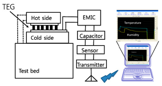
Figure 1.
The proposed wireless sensor node system for environmental monitoring application with temperature and humidity sensor.
3. Thermoelectric Generator
3.1. TEG Device Fabrication Process
For arraying, mass production, and industrialization of 3-D thermoelectric devices, top-down method based on Complementary Metal-Oxide Semiconductor (CMOS) process should be used instead of bottom-up process. For this, as shown in Figure 2, a 675 µm thick wafer was repeatedly laminated with Pt (platinum)-silicide and silicon on a substrate, and finally a structure in which Pt-silicide and silicon were repeated was fabricated by heat treatment. The thickness of the structure was made to have a thickness of 50 nm for each of Pt-silicide and silicon, and a repetitive structure of up to 12 layers was formed. As a result, it is possible to obtain a higher Seebeck coefficient and power factor than pure silicon by forming an energy barrier as the Pt-silicide having the nano thickness is repeatedly positioned in the vertical direction of the device. In this experiment, boron and arsenic were used to make the p-type and n-type wafer respectively resulting in resistivity of <0.005 Ω·cm. Si should be thicker than the Pt to fabricate the multilayer structure with same thickness because the volume increase when the Pt reacts with Si, therefore Pt and the Si are sputtered with 16 nm and the 80 nm, respectively, to form a 50 nm period [20]. Silicide reaction was conducted by rapid thermal process at 500 °C, 5 min. To prevent the Schottky barrier between both ends of the leg and solder paste, both ends were covered with 300 nm of gold and a 10 nm titanium adhesion layer. After the completion of deposition process, the wafer was diced with 1.4 mm × 1.4 mm.
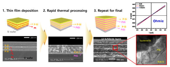
Figure 2.
Fabrication process of the Silicon based thermoelectric device.
Figure 3a,c shows the change in Seebeck coefficient measured according to temperature when the pt-Si 12 layers were laminated. Figure 3b,d shows the change of Seebeck coefficient according to the change of the number of laminated layers under each temperature condition. These figures mean that the Seebeck coefficient increases as the number of repeated layers increases. The Seebeck coefficient has a value of about 240 uV/K at 420 K for N/P-type bulk silicon and about 280 uV/K for 12 layers. This is because only electrons and holes having relatively high energy can be moved by the Schottky barrier at the silicide/silicon interface when electrons and holes in the high temperature region move in the silicide/silicon structure proposed in this study [20]. In addition, as shown in Figure 3a,c, it can be seen that the power factor has a very high value in the case of silicon. The maximum value of the measured N/P-type three-dimensional thermoelectric power factor was 12 mW/mK2 and 9.9 mW/mK2, respectively. From this, it can be seen that silicon is a suitable material for the application of the Thermoelectric Generator (TEG) for thermal power generation.
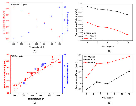
Figure 3.
Seebeck coefficient and power factor of three-dimensional n-type thermoelectric materials according to (a) temperature and (b) layer numbers, and Seebeck coefficient and power factor of three-dimensional p-type thermoelectric materials according to (c) temperature and (d) layer numbers.
3.2. TEG Module Fabrication and Measurement
Figure 4 shows a silicon-based three-dimensional thermo-electric module 4a, fabrication overview 4b and fabrication process details 4c. In Figure 4b, the thermoelectric material and the upper substrate are placed on the lower substrate patterned in the shape of an electrode, and the hybrid cu paste to be described later is placed. By applying pressure and heat to them, a very stable bonding can be achieved thermally, electrically, and mechanically. The actual fabrication process 4c is as follows. First, a three-dimensional silicon thermoelectric material is fabricated and then cut into a square of 1.4 mm in size. The cut thermoelectric materials are placed on the substrate on which the electrodes are disposed, and after the paste is deposited, they are connected together by the required temperature and pressure. This completes the thermoelectric module fabrication process. For manufacturing processes of the commercial thermoelectric module, heat flow during the paste curing process cannot be effectively applied due to the pastes with low thermal conductivity and the ceramic substrates with low thermal conductivity [28]. In order to solve this problem, silicon substrates were used instead of ceramic substrates, and a technology for simultaneously performing thermal, electrical, and mechanical bonding by using commercial high temperature high thermal conductive pastes or melting and connecting aluminum thin films was developed. This technology is the result of advancement of existing packaging technology for silicon thermoelectric devices, and it can be expected to improve the efficiency by increasing the thermal conductivity of the substrate and the contact quality of the paste.
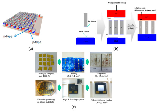
Figure 4.
(a) The 3D thermoelectric module based on Silicon and (b) the fabrication overview. (c) Fabrication process details of the thermoelectric module.
For the thermal and electrical interconnections between a thermoelectric device and upper and lower substrates, Hybrid Cu paste (HCP) was used. The HCP material, composed of a thermosetting resin, Ag-coated Cu, and Sn/3.0Ag/0.5Cu solder powders, was developed and introduced in previous research [29]. Table 1 shows the composition of components and thermal conductivity of cured HCP. The specific curing process is as follows. First, the paste material was printed on the electrodes of the upper and lower substrates using a screen printing process. Second, n-type and p-type hetero-structure Si legs were placed on the pasted electrodes. Third, the top substrate was aligned and pre-bonded using a flip-chip bonder. Finally, the thermoelectric module was cured according to the curing conditions of the HCP. When using commercially available Ag paste, it took 2 h at 230 °C to cure, but the developed HCP cured at 240 °C in 10 min after the printing process.

Table 1.
Composition of components and thermal conductivity of cured Hybrid Cu paste (HCP) used.
Figure 5 shows the output characteristics of the commercial Bi2Te3 thermoelectric module, the commercial packaging thermoelectric module using a ceramic substrate, and the optimized silicon thermoelectric module fabricated in this study. Through packaging optimization, we can see the performance improvement more than 70 times, and the improved value is almost close to the value of Bi2Te3 which is used as a commercial device. In high temperature operation, it is expected to bring efficiency beyond commercial components like Bi2Te3. Since most packaging pastes start to denature at temperatures above 300 degrees, further optimization studies for high temperature operation need to be conducted.
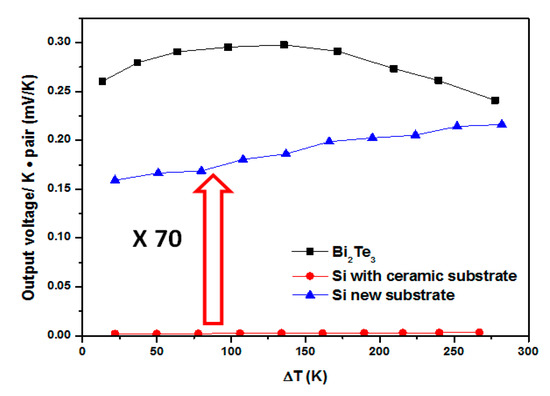
Figure 5.
Output measurement results of the commercial Bi2Te3 thermoelectric module, the commercial thermoelectric module using a ceramic substrate, and the optimized silicon thermoelectric module.
Commercial products usually contain more than 100 pairs of thermoelectric materials in one module [30], which is a major obstacle to commercialization unless a large number of thermoelectric materials are manufactured in one batch during material fabrication. Therefore, the processes for silicon thermoelectric material fabrication and module fabrication need to be developed to be suitable for mass production processes. For this purpose, we developed a 6inch silicon fabrication process and developed a technology to fabricate a large number of thermoelectric materials in one batch. The development process for mass production is shown in Figure 6. First, a Pt-Si layer is formed on the upper and lower surfaces of the wafer doped appropriately, and 300 nm of Au is deposited to minimize the thermal and electrical contact resistance. The silicon wafer is annealed at 300 °C, and then diced into the desired size. In this task, the size is basically 1.4 mm × 1.4 mm. These cut materials are peeled off adhesive tape, washed with Acetone and Methanol, and then applied to the module assembly. In order to assemble these materials together on a substrate and keep the distance between each material constant, p-type Si legs are placed on the dedicated home-made jig. The HCP solder paste was screen printed on the bottom substrate of the thermoelectric module with pre-patterned electrodes. The aligned jigs with p-type Si legs are put on the above substrate with solder paste and the substrate with legs are hot pressed with 240 °C in 10 min. n-type Si legs are placed on the dedicated home-made jig. The HCP solder paste was screen printed on the upper substrate of the thermoelectric module with pre-patterned electrodes. The aligned jigs with n-type Si legs are put on the upper substrate with solder paste and the substrate with legs are hot pressed with 240 °C in 10 min. Then, the bottom substrate with p-type Si legs are aligned with upper substrate with n-type Si legs by using home-made fabrication set-up and are hot pressed with 240 °C in 10 min. After a series of verification work, the developed module is used to evaluate the performance using the characterization system developed in this study.
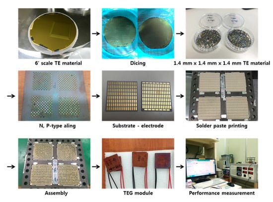
Figure 6.
The fabrication process Si thermoelectric module with Si substrate for mass production process.
In general, a thermoelectric evaluation system is composed of basic temperature control function, heat dissipation structure, and electrical characteristic measurement module. However, the silicon thermoelectric element has a relatively high thermal conductivity, which causes a local temperature difference in the heating plate or the cooling plate. Therefore, the contact thermal resistance between them negatively affects the entire system, so it must be measured while reducing the error. Figure 7 is an actual photograph of a silicon-based 3D thermo-element evaluation system that has been redesigned in consideration of this. It was designed to collect the measurement data in real time unlike the initially developed silicon thermoelectric module measuring device. In order to make the contact thermal resistance of the thermoelectric module and the heating plate/cooling plate as equal as possible for each experimental group, three springs in a vertical direction were set up so that heat could be applied at a constant pressure. In addition, by increasing the capacity of the heating heater, it is possible to evaluate the high-temperature performance of the silicon material with higher performance at high temperature. In order to directly calculate the power depending on the load resistance to be connected to the module, the external resistance to the external device is modeled so that the power according to the external resistance can be measured at one time. In the case of temperature control, the existing evaluation system uses the relay, which causes the temperature to fluctuate continuously about ±2–3 °C from the target temperature. However, in this system, the temperature is kept constant without changing so that accurate thermoelectric properties can be measured.
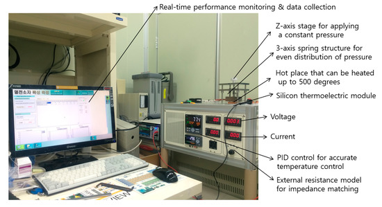
Figure 7.
The evaluation set-up for 3D thermoelectric module.
Figure 8a–d shows performances of the thermoelectric module measured with the thermoelectric module evaluation system. First, the output characteristics of the module was checked by measuring the voltage according to the temperature while the module was opened, in Figure 8a. At this time, the generated power was calculated using the value obtained by measuring the resistance of the module by connecting various resistors to the outside. If a general ohmmeter is used to extract the resistance value, the current generated to measure the resistance causes a peltier effect, or the resistance measured by the Seebeck voltage already generated in the module has an error. To prevent this, when measuring the resistance, the internal resistance of the power generation part can be measured more accurately by connecting the reference resistor to the outside and measuring the voltage applied to the resistor. Figure 8b shows the result of evaluating the output characteristics through the I-V relationship by connecting the module to various external resistors. The temperature difference of about 70 K allowed the module to produce up to 10 mW. Figure 8c is a graph comparing the thermoelectric properties of silicon with commercial materials. For Bi2Te3 materials used as commercial thermoelectric materials, the performance tends to decrease sharply with high temperatures. On the other hand, in the case of silicon, the voltage tends to increase steadily as temperature increases, and in the region where the temperature difference is more than 250 K, it is higher than the voltage of commercial materials. Figure 8d shows the output power according to the temperature difference and shows a similar trend to Figure 8c.
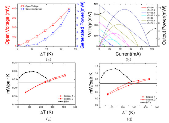
Figure 8.
The performance of the fabricated thermoelectric module: (a) open circuit voltage and power of thermoelectric module according to the temperature, (b) output characteristics of thermoelectric module according to the temperature, (c) comparison of Voltage characteristics with commercial thermoelectric modules, (d) comparison of power characteristics with commercial thermoelectric modules.
4. Energy Management IC for Silicon TEG
4.1. Proposed Energy Management IC
Figure 9 shows the structure of the proposed EMIC, and Table 2 shows internal voltage values used in the proposed EMIC. In order to drive low power IOT and WSN system with thermoelectric energy harvesting, EMIC requires the following three conditions in addition to high efficiency: MPPT, cold start, and self-power capability. First, the energy obtained from the TEG should be sent to the output as much as possible. To achieve this, the circuit requires MPPT as well as a high efficiency. MPPT function is to perform the impedance matching to transfer the energy harvested from the TEG to the EMIC as much as possible, thereby continuously sensing the impedance of the TEG and adjusting the impedance of the EMIC to be equal to it. As described in [31], the basic principle of operation is to open the TEG by blocking the current path through the EMIC to detect the open circuit voltage of the TEG in sense mode. After that, the duty is automatically changed through a designed feedback loop so that the input voltage of the EMIC follows the half voltage of VTEG in operating mode. This method, called fractional open circuit voltage (FOCV) MPPT, is suitable for low-power applications because it can be realized by simple circuit structure and consumes less power and has higher transfer efficiency. In this circuit, we added an on-chip MPPT period controller that can be controlled by adjusting the reference voltage (VRC1, VRC2) or capacitors (C1, C2) values in Figure 10, compared with the external clock source [27]. The MPPT period can be adjusted according to the environment change and the power consumption was reduced by applying a structure to reduce the standby power loss as much as possible. The Maximum input power to EMIC, PMPP can be obtained as the following equation from [31].
where VTEG and RTEG are the open circuit voltage and internal impedance of TEG, and VIN is the input voltage of the EMIC, and PMPP is the input power at MPP condition.
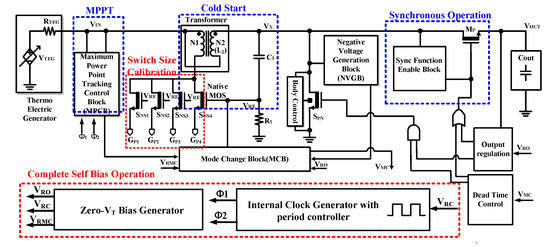
Figure 9.
The proposed energy management integrated circuit (EMIC) block diagram.
Table 2.
Internal voltage values in the proposed EMIC.
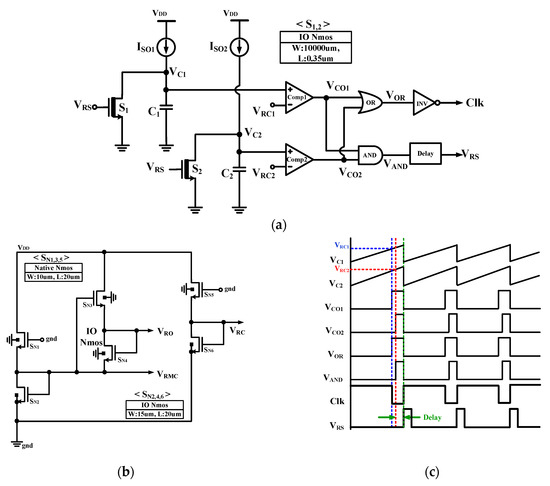
Figure 10.
The proposed (a) on-chip MPPT period controller, (b) on-chip reference generator, and (c) the detailed operation waveforms of on-chip MPPT period controller.
The second is a self-start-up function called cold start. If the power required for the output is greater than the power that can be generated at the input, the circuit is turned off. However, if the power supplied from the input again exceeds the power required for the output, the circuit must be able to start of itself. Especially for thermoelectric energy harvesting, the output voltage level is low, unlike solar energy harvesting, so it must start even at voltages below the minimum threshold voltage of the CMOS process. This becomes an important issue in thermoelectric energy harvesting system. In this study, a cold start is constructed based on the high turn ratio transformer of [25]. The transformer, B82801C of TDK is a current sense type which has low DCR, and the turn ratio is 1:50. However, in [25,26,27], the leakage power by the configuration of the transformer and native switch can be further increased due to the Process-Voltage-Temperature (PVT) variation. Therefore in this study, the native switch size calibration is added to reduce leakage power from the PVT variation.
Finally, mass-produced products for thermoelectric energy harvesting need complete self-power capability for application in variety of environments. In particular, in order to apply to an environment in which the human cannot reach or the battery cannot be used, reference and clock signals should be generated by supplying power only from the input TEG, not by an external voltage. In the conventional circuit [25,26,27], the external power source was used because a stable reference voltage could not be generated in cold start process. The external clock for impedance matching control was used to verify the optimum operating point for changes in the surrounding environment. In this study, we propose an on-chip MPPT period controller and on-chip reference generator that replaces the external clock and voltages in Figure 10a,b. The on-chip MPPT period controller has a simple structure that generates clock signals for MPPT operation with very low power consumption and can be adjusted to various periods as desired by adjusting the capacitor size and VRC. The on-chip reference generator has obtained the required voltage by optimizing the Transistor (TR) size for use with low error in a wider voltage range (0–3.3 V) than the supply voltage range (0–0.5 V) of the conventional circuit [32]. Figure 10c shows the detailed operating waveforms of on-chip MPPT period controller. This additional works extended the utilization range and achieved a complete self-power circuit compared to [25,26,27].
The chip micrograph of the proposed EMIC is shown in Figure 11. It consists of power switches, native switches, control logics and self-bias parts.
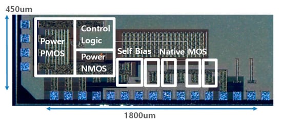
Figure 11.
The chip micrograph of the proposed EMIC.
4.2. Energy Management IC Measurement Results
In order to verify the operation of the cold start and the MPPT, we measured EMIC and presented the results in Figure 12. Figure 12a shows the results of cold start measurements. In the initial state, the voltage is not applied and the input voltage is 0 V. When the input voltage reaches 200 mV, the output voltage increases as the oscillation increases at the node Vx, through the designed feedback loop. When the output rises to 0.7 V or more, the start-up mode is switched to the boost mode and the output is increased to 3 V. Even if EMIC is stopped due to sudden changes in the external environment, an input or an output, it can be restarted of itself at input voltages of 200 mV and above. Figure 12b shows the measurement results of MPPT operation. When CLK is low, VTEG 200 mV is sensed and when CLK is high, the input of VIN, 100 mV is maintained while transferring power in MPP condition. The output voltage can be adjusted to the desired voltage in the range of 1 V to 3 V. Figure 12b,c shows that the MPPT period controller is working as designed. In applications where the external environment changes very rapidly, the sensing cycle is shortened to maintain the MPP state, whereas in applications where the external environment changes slowly, the sensing cycle is extended to minimize the loss. In the former case, the energy loss is large because there are few ranges where energy is transferred, while in the latter case, energy loss is small because energy is delivered in most of the ranges.
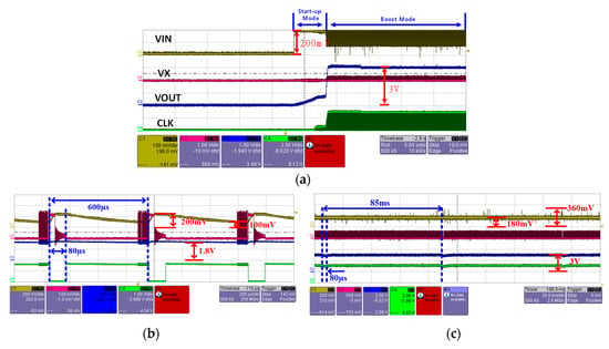
Figure 12.
The waveforms of (a) the cold start operation, (b) the MPPT operation, and (c) MPPT period controller operation.
Figure 13 shows the EMIC measurement environment and efficiency measurement set-up. To measure the efficiency of EMIC accurately, we used electrical model of TEG consisting of a power supply and resistor, instead of TEG [33]. The input voltage was set to 300 mV and ZTEG, the internal impedance of the TEG, was measured at 5.7 Ω. The input power of the EMIC is obtained by measuring the current and voltage through the power supply and the multi-meter on the input side, and the output power of EMIC is obtained by measuring the output voltage and current of the load through the electric load.
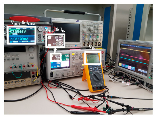
Figure 13.
The EMIC measurement environment and efficiency measurement set-up.
Table 3 shows the power efficiency of the proposed EMIC in all input voltage range. The peak efficiency (η), about 78.7% was obtained, and the MPPT efficiency (ηM), about 99.4% was obtained.
Table 3.
Power efficiency of the proposed EMIC.
5. Self-Powered Autonomous Wireless Sensor Node
In order to test whether the power generated by the proposed silicon thermoelectric module and EMIC is applicable to IOT and WSN applications, we proposed RF module with an low power Bluetooth module, a temperature and humidity sensor, and MCU. Then we verified whether the wireless sensor node consisting of these thermoelectric module, EMIC, RF module, and display, works properly with generated power only.
5.1. Proposed RF Module with Bluetooth Module, MCU, and Sensor
The left side of Figure 14 shows a Transmitter (TM) module consisting of Bluetooth module, temperature and humidity sensor, and MCU, and the right side of Figure 14 shows a Receiver (RC) module connected with a laptop. The Bluetooth communication uses version 4 to transmit information to minimize energy consumption.
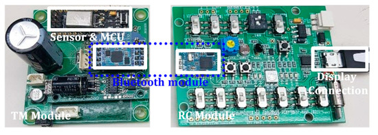
Figure 14.
A low power Radio Frequency (RF) module with a Bluetooth module (BoT-CLE100), temperature and humidity sensor (HT01DL), and MCU (atmega16L).
The charging time of one cycle for the temperature and humidity sensing was set as the time that the power delivered from the thermoelectric module can sufficiently operate the TM module. And a detection resolution for temperature and humidity was set to 1 degree and less than 1% to be available for various application environments. A simple analysis to find the charging time of one cycle is shown in the next section.
5.2. Autonomous Wireless Sensor Node System
The experimental set-up for verifying the feasibility of the proposed wireless sensor node system is shown in Figure 15. The self-made thermo-exciter was used to supply reliable temperature difference of 70 K to the device. The heating block in the thermos-exciter was controlled by Yokogawa temperature controller. The temperature sensor was located in the heating block and cooling block and used to measure the temperatures of the hot and cold side in the device. The measured temperatures from the sensors and the output voltage of the device were displayed on the test bed, digital multi-meter, oscilloscope, etc. The generated power by our thermoelectric energy generator based on Si legs was converted and regulated by the proposed EMIC. The details of EMIC power conversion and some results of that were shown in Section 4. The output power of EMIC can be stored in a variety of capacitors, ranging from tens of nF capacitor to large supercapacitors larger than 1F. In this experiment, a 10 uF capacitor was used as the storage to verify the operation with proper measurement time. After the EMIC charges the output capacitor to the voltage at which the Bluetooth module and the temperature and humidity sensor operate, it supplies power to the TM module with the temperature and humidity sensor. Then, temperature and humidity information are detected in real time, transmitted to the RC module, and the transmitted information is displayed on the laptop through a self-designed program.
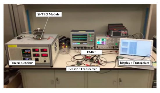
Figure 15.
The experimental set-up for verifying the feasibility of the proposed wireless sensor node system.
Figure 16 shows the temperature and humidity graph and data measured by the wireless sensor node system proposed in this study. The upper left shows the temperature graph, the lower left shows the humidity graph, and the temperature and humidity are changed by blowing the temperature humidity sensor. During the initial few seconds, the initialization process causes the value to change significantly and soon detects the temperature and humidity of the environment and converges to a specific value. After that, when the temperature and humidity increase rapidly during the blowing and the influence of the blowing disappears, it returns to the original value.
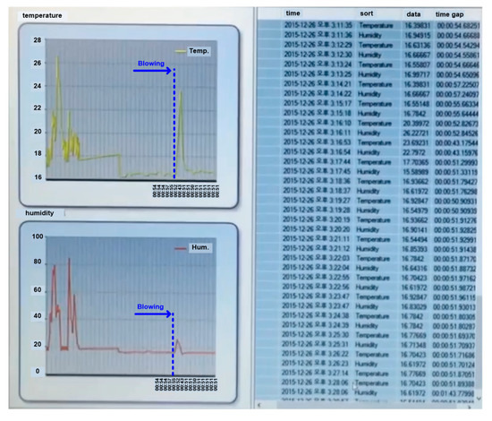
Figure 16.
The temperature and humidity graph and data measured by the wireless sensor node system.
The charging time of one cycle is determined by relationship between the input power, EMIC Loss, and the standby/operating power of the TM module. Therefore, when setting the charging time according to the given environment, it is necessary to take into account the input power and power consumption of each component. The following Table 4 and Equation (2) are a brief analysis of the determination of the charging time of one cycle.
Table 4.
I/O power and power consumption of each component.
Looking at the graph in Figure 16 above, we can see that the time gap of each data is maintained around 50 s.
5.3. Rechargeable Battery Charging Experiment with 3D Silicon TEG
In addition to the (super) capacitor used in the experiment as the storage, the experiment was conducted to charge the battery. Battery charging experiments are important because they can be used as auxiliary power to save excess energy, and can prove their usefulness in battery-critical environments. Figure 17 shows the Li-ion battery charge settings. The nominal voltage and the capacity of the Li-ion battery were about 2.4–2.8 V and 1.0 mAh, respectively. The temperature difference is applied to the thermoelectric module by the test bed. The output lead wire is connected to the EMIC module that converts the voltage to match the charging voltage of the battery. Real-time charging voltages can be observed by the multi-meter.
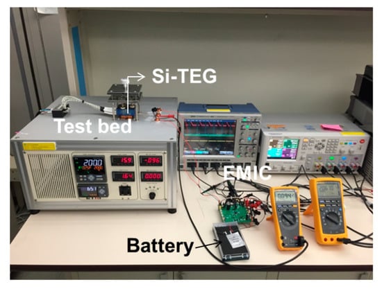
Figure 17.
The Li-ion battery charging setup.
Figure 18 shows the charging and discharging curves of a Li-ion battery in 0.2 C Constant Current (cc) mode by external power source, and the charging curve through the proposed Si-TEG and EMIC. The time needed for 1.0 mAh Li-ion battery full-charging by using our thermoelectric energy harvester under ∆T = 135 K condition was about 1 h. The charging voltage is recorded in real time, and displayed as a graph. The charging operation by SI-TEG and EMIC was performed in a higher current mode than that of external power source. As shown in Figure 18, we can see that the charging speed is about 5 times faster than 0.2 C cc mode, and verified that the proposed SI-TEG and EMIC module work normally on battery charging.
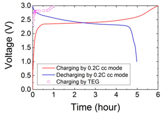
Figure 18.
The charging and discharging curves of a Li-ion battery in 0.2 C cc mode by external power source and the charging curve through the proposed Si-TEG and EMIC.
6. Conclusions
We demonstrate the silicon based energy harvesting system consisting of hetero-structured silicon thermoelectric module generating energy, EMIC managing the power and a low power RF module for the application of WSN and IOT. Hetero-structure, which is known for enhancing properties of thermoelectric power more than pure silicon, is successfully applied to the module with appropriate solder and the electrode design. Thermoelectric properties of each material and the module were measured by the self-made measuring system which is improved for the better mechanical contact. EMIC converts the low input voltage to the desired high voltage with high efficiency and performs the impedance matching to transfer the energy harvested from the TEG to the EMIC as much as possible. Finally, we demonstrated the proposed sensor node system which can transmit and monitor the information from the temperature and humidity sensor through the RF module in real time, and verified feasibility of that for variable applications. The proposed system can be applied to the industrial IOT environment. Especially, it can monitor various environments including temperature, humidity, gas, and stress, in real time by utilizing the waste heat generated from the high temperature difference of more than 70 degrees of boiler steam piping in a smart factory.
Author Contributions
Conceptualization, J.-P.I. and S.E.M.; methodology, J.-P.I. and J.H.K.; investigation, J.W.L., J.Y.W., S.Y.I. and Y.K.; writing—original draft preparation, J.-P.I. S.E.M.; writing—review and editing, J.-P.I., Y.-S.E., W.C.C. and J.S.K.; supervision, S.E.M.; project administration, S.E.M. All authors have read and agreed to the published version of the manuscript.
Funding
This work was supported by the National Research Council of Science & Technology (NST) grant by the Korea government (MSIP) (No. CAP-14-01-KIST), by the Materials and Components Technology Development Program of MOTIE/KEIT, Republic of Korea (No. 10063286, Development of high efficient thermoelectric module with figure of merit (Z) 3.4(×10−3) by using 1.0 kg per batch scale producible polycrystalline thermoelectric material with average figure of merit (ZT) 1.4 and over”).
Conflicts of Interest
The authors declare no conflict of interest.
References
- Tiwari, H.D.; Kim, J.H. Novel Method for DNA-Based Elliptic Curve Cryptography for IoT Devices. ETRI J. 2018, 40, 396–409. [Google Scholar] [CrossRef]
- Yoon, Y.S.; Zo, H.; Choi, M.; Lee, D.; Lee, H.W. Exploring the Dynamic Knowledge Structure of Studies on the Internet of Things: Keyword Analysis. ETRI J. 2018, 40, 745–758. [Google Scholar] [CrossRef]
- Cicioğlu, M.; Çalhan, A. SDN-based wireless body area network routing algorithm for healthcare architecture. ETRI J. 2019, 41, 452–464. [Google Scholar] [CrossRef]
- Dong, Y.; Wang, T.; Li, S.; Cui, M.; Wu, H. Energy Harvesting Technologies for Tire Pressure Monitoring Systems. ETRI J. 2019, 41, 326–336. [Google Scholar] [CrossRef]
- Roundy, S.; Wright, P.K. A Piezoelectric Vibration Based Generator for Wireless Electronics. Smart Mater. Struct. 2004, 13, 1131–1142. [Google Scholar] [CrossRef]
- Kang, T.; Kim, J.; Park, S.; Son, K.; Park, K.; Lee, J.; Kang, S.; Choi, B. Evaluation of a Betavoltaic Energy Converter Supporting Scalable Modular Structure. ETRI J. 2019, 41, 254–261. [Google Scholar] [CrossRef]
- Hudak, N.S.; Amatucci, G.G. Small-Scale Energy Harvesting Through Thermoelectric, Vibration, and Radiofrequency Power Conversion. J. Appl. Physics 2008, 103, 101301–101324. [Google Scholar] [CrossRef]
- Kim, M.Y.; Oh, T.S.; Kim, J.S. Annealing Behavior of Bi2Te3 Thermoelectric Semiconductor Electrodeposited for Nanowire Applications. J. Korean Phys. Soc. 2007, 50, 670–676. [Google Scholar]
- Liu, H.; Zhong, J.; Lee, C.; Lee, S.W.; Lin, L. A comprehensive review on piezoelectric energy harvesting technology: Materials, mechanisms, and applications. Appl. Physics Rev. 2018, 5, 041306. [Google Scholar] [CrossRef]
- Shi, Q.; He, T.; Lee, C. More than energy harvesting—Combining triboelectric nanogenerator and flexible electronics technology for enabling novel micro-/nano-systems. Nano Energy 2019, 57, 851–871. [Google Scholar] [CrossRef]
- Wang, J.; He, T.; Lee, C. Development of neural interfaces and energy harvesters towards self-powered implantable systems for healthcare monitoring and rehabilitation purposes. Nano Energy 2019, 65, 104039. [Google Scholar] [CrossRef]
- Haras, M.; Skotnicki, T. Thermoelectricity for IoT—A review. Nano Energy 2018, 54, 461–476. [Google Scholar] [CrossRef]
- Yan, J.; Liao, X. Review of Micro Thermoelectric Generator. IEEE JMEMS 2018, 27, 1–18. [Google Scholar] [CrossRef]
- Petsagkourakis, I.; Tybrandt, K.; Crispin, X.; Ohkubo, I.; Satoh, N.; Mori, T. Thermoelectric materials and applications for energy harvesting power generation. STAM 2018, 19, 836–862. [Google Scholar] [PubMed]
- Liu, H.; Zhang, J.; Shi, Q.; He, T.; Chen, T.; Sun, L.; Dziuban, J.A.; Lee, C. Development of a Thermoelectric and Electromagnetic Hybrid Energy Harvester from Water Flow in an Irrigation System. Micromachines 2018, 9, 395. [Google Scholar] [CrossRef] [PubMed]
- Kim, S.J.; We, J.H.; Cho, B.J. A wearable thermoelectric generator fabricated on a glass fabric. Energy Environ. Sci. 2014, 7, 1959. [Google Scholar] [CrossRef]
- Xie, J.; Lee, C.; Wang, M.F.; Feng, H. Seal and encapsulate cavities for CMOS MEMS thermoelectric power generators. J. Vacuum Sci. Technol. B 2011, 29, 021401. [Google Scholar] [CrossRef]
- Kao, P.H.; Shih, P.J.; Dai, C.L.; Liu, M.C. Design, Fabrication and characterization of CMOS MEMS-Based Thermoelectric Power Generators. IEEE/ASME J. Microelectromech. Syst. 2010, 19, 317–324. [Google Scholar]
- Xie, J.; Lee, C.; Liu, Y.; Wang, M.F.; Skotnicki, T. Characterization of heavily doped polysilicon films for CMOS-MEMS thermoelectric power generators. J. Micromech. Microeng. 2009, 19, 125029. [Google Scholar] [CrossRef]
- Choi, W.; Jun, D.; Kim, S.; Shin, M.; Jang, M. Thermoelectric characteristics of Pt-silicide/silicon multi-layer structured p-type silicon. Energy 2015, 82, 180–183. [Google Scholar] [CrossRef]
- Watanabe, T. Silicon-based Micro Thermoelectric Generator Fabricated by CMOS Compatible Process. In Proceedings of the 2017 IEEE International Meeting for Future of Electron Devices, Kansai (IMFEDK), Kyoto, Japan, 29–30 June 2017. [Google Scholar]
- Perez-Marín, A.P.; Ferrando, P.; Lopeandía, A.F.; Garcia, G.; Abad, L.; Lopez, A.M.; Muñoz-Pascial, F.X.; Rpdrígiez-Viejo, J. Micropower thermoelectric generator from thin Si membranes. Nano Energy 2014, 4, 73–80. [Google Scholar] [CrossRef]
- LTC3108 Datasheet, Linear Tech. Available online: https://www.analog.com/media/en/technical-documentation/data-sheets/LTC3108.pdf (accessed on 1 October 2019).
- TI bq25504 Datasheet, Texas Ins. Available online: http://www.ti.com/lit/ds/symlink/bq25504.pdf (accessed on 1 October 2019).
- Im, J.P.; Moon, S.E.; Lyuh, C.G. Transformer-Reuse Reconfigurable Synchronous Boost Converter with 20 mV MPPT-Input, 88% Efficiency, and 37 mW Maximum Output Power. ETRI J. 2016, 38, 654–664. [Google Scholar]
- Im, J.P.; Wang, S.W.; Lee, K.H.; Woo, Y.J.; Yuk, U.S.; Kong, T.H.; Hong, S.W.; Ryu, S.T.; Cho, G.H. A 40 mV transformer-reuse self-startup boost converter with MPPT control for thermoelectric energy harvesting. In Proceedings of the 2012 IEEE International Solid-State Circuits Conference, ISSCC 2012, San Francisco, CA, USA, 19–23 February 2012; pp. 104–105. [Google Scholar]
- Im, J.P.; Wang, S.W.; Ryu, S.T.; Cho, G.H. A 40 mV Transformer-Reuse Self-Startup Boost Converter with MPPT Control for Thermoelectric Energy Harvesting. IEEE J. Solid-State Circuits 2012, 47, 3055–3067. [Google Scholar] [CrossRef]
- FerroTec. Available online: http://www.ferrotec-global.com/tech_2_2.php?lang=en (accessed on 28 January 2020).
- Eom, Y.-S.; Choi, K.-S.; Moon, S.-H.; Park, J.H.; Lee, J.H.; Moon, J.T. Characterization of a Hybrid Cu Paste as an Isotropic Conductive Adhesive. ETRI J. 2011, 33, 864–870. [Google Scholar] [CrossRef]
- Livingcare Development. Available online: http://lcdm.co.kr/ (accessed on 28 January 2020).
- Cho, S.K.; Kim, N.; Park, S.; Kim, S. A Coreless Maximum Power Point Tracking Circuit of Thermoelectric Generators for Battery Charging Systems. In Proceedings of the 2010 IEEE Asian Solid-State Circuits Conference, Beijing, China, 8–10 November 2010; pp. 1–4. [Google Scholar]
- Seok, M.; Kim, G.; Blaauw, D.; Sylvester, D. A Portable 2-Transistor Picowatt Temperature Compensated Voltage Reference Operating at 0.5 V. IEEE J. Solid-State Circuits 2012, 47, 2534–2545. [Google Scholar] [CrossRef]
- Ramadass, Y.K.; Chandrakasan, A.P. A Battery-Less Thermoelectric Energy Harvesting Interface Circuit With 35 mV Startup Voltage. IEEE J. Solid-State Circuits 2011, 46, 333–341. [Google Scholar] [CrossRef]
© 2020 by the authors. Licensee MDPI, Basel, Switzerland. This article is an open access article distributed under the terms and conditions of the Creative Commons Attribution (CC BY) license (http://creativecommons.org/licenses/by/4.0/).