Experimental Evidence of PID Effect on CIGS Photovoltaic Modules


 and
and 
Abstract
1. Introduction
2. Diagnostics Techniques for PID Detection
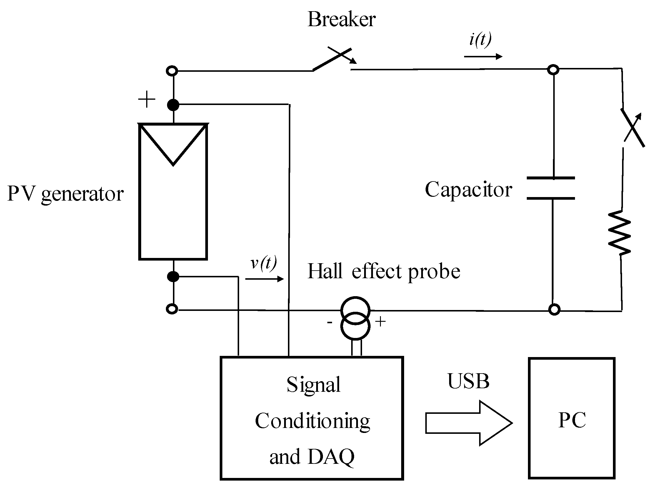
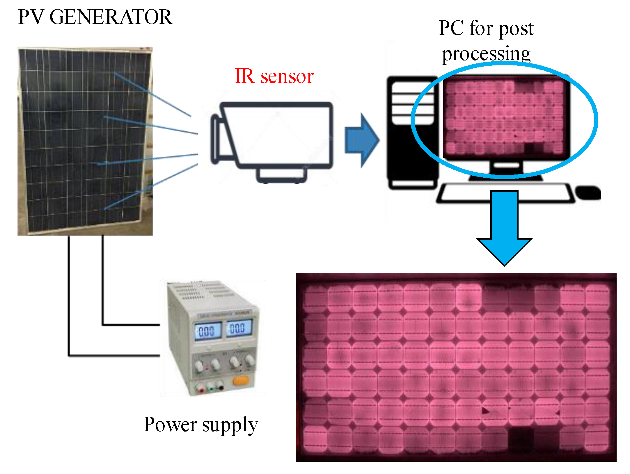
2.1. Description of Diagnostics Techniques for Defects Detection
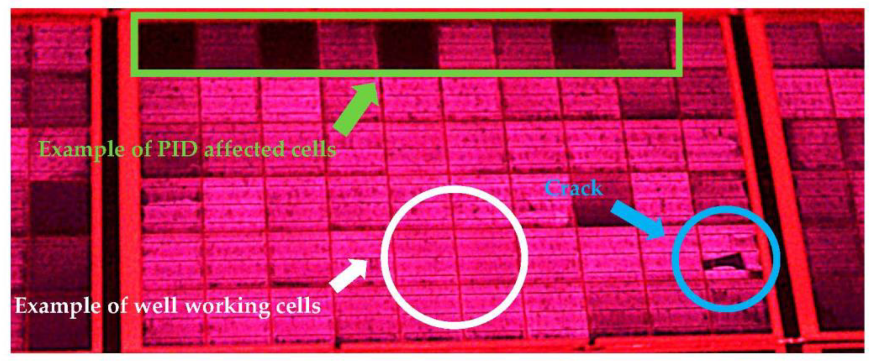
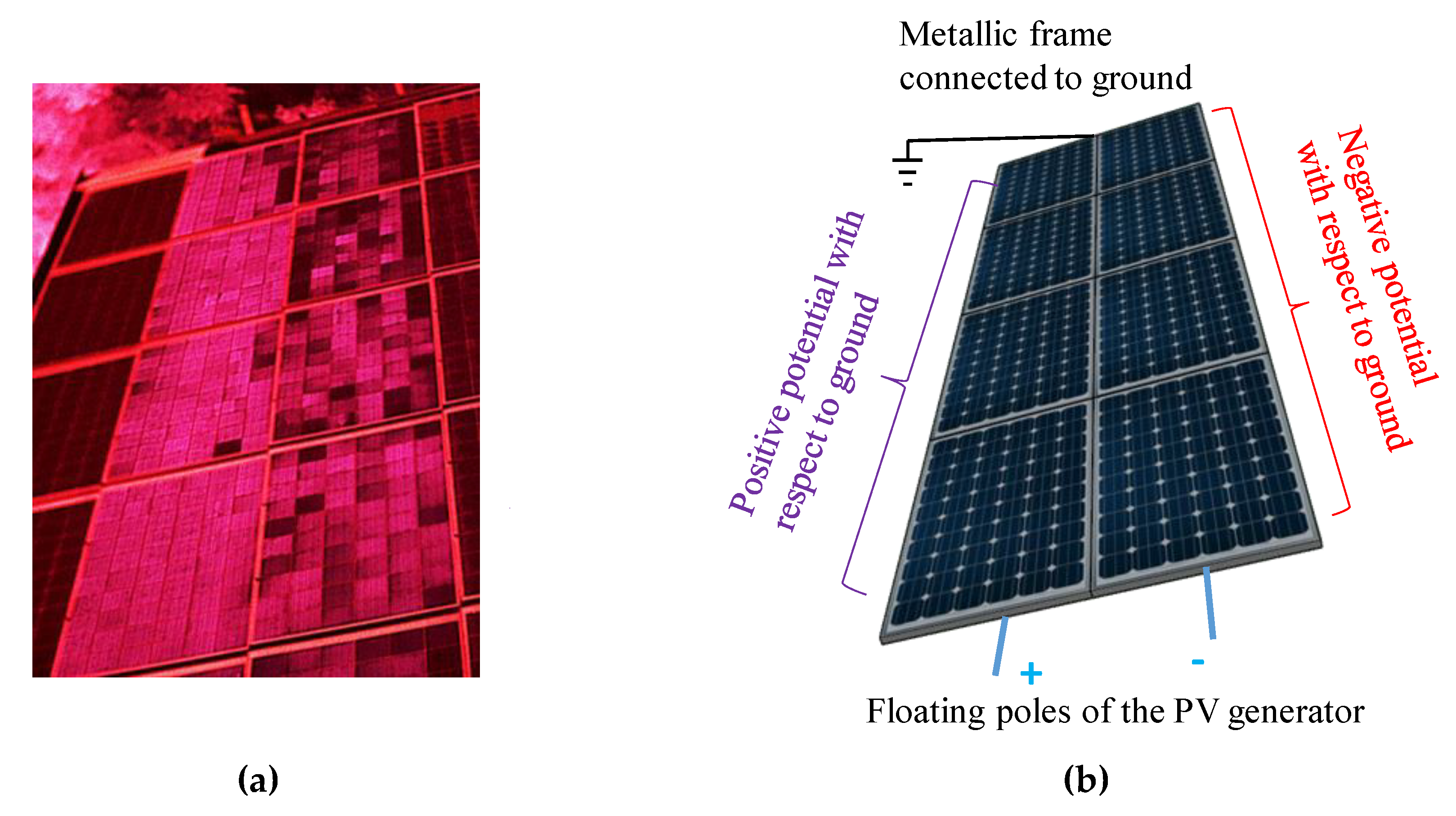
2.2. Detection of PID
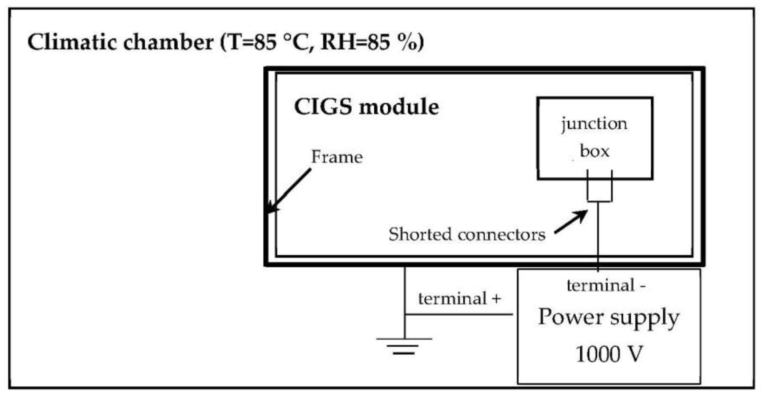
3. Experimental Setup
3.1. Degradation
3.2. Recovery
4. Results and Discussion
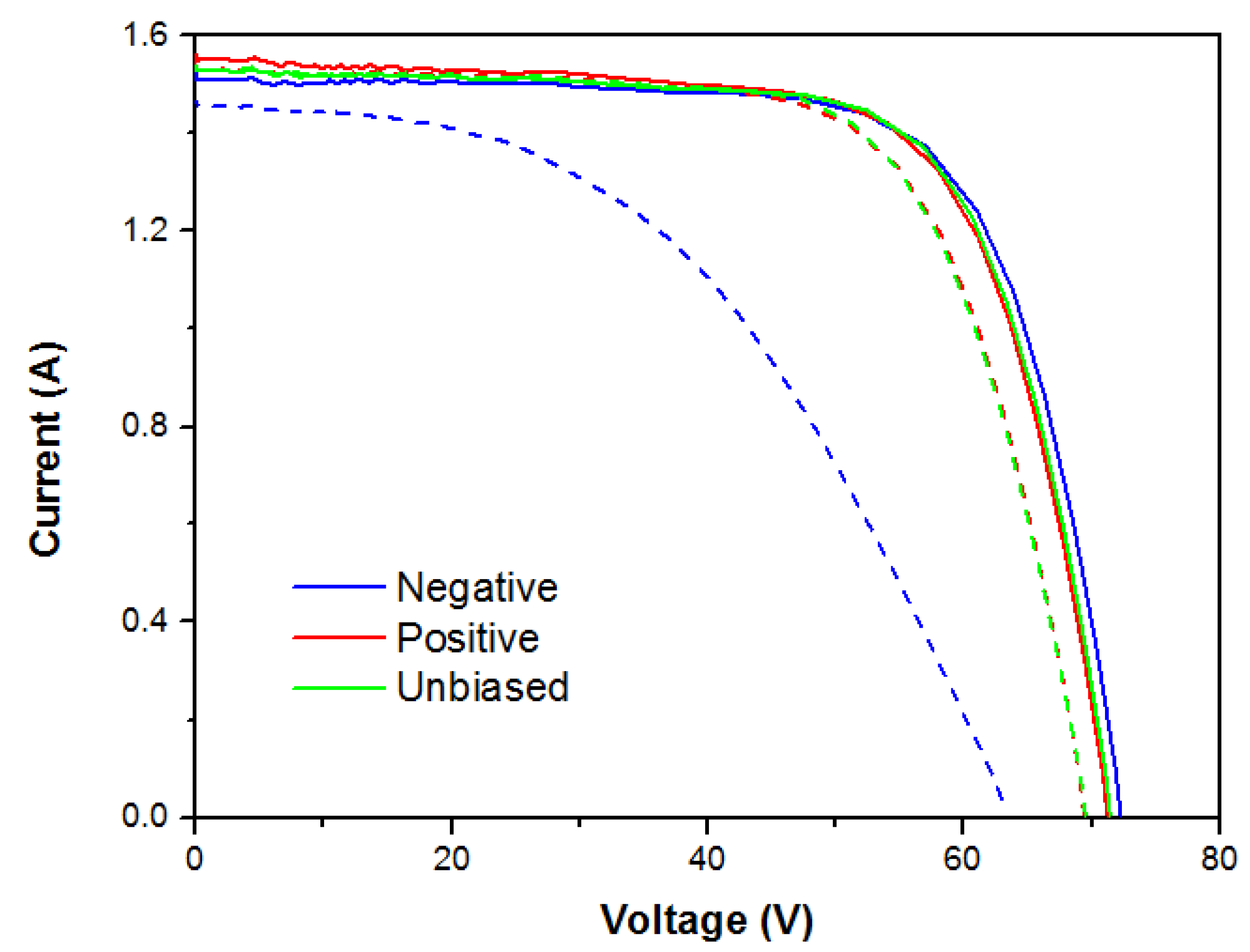
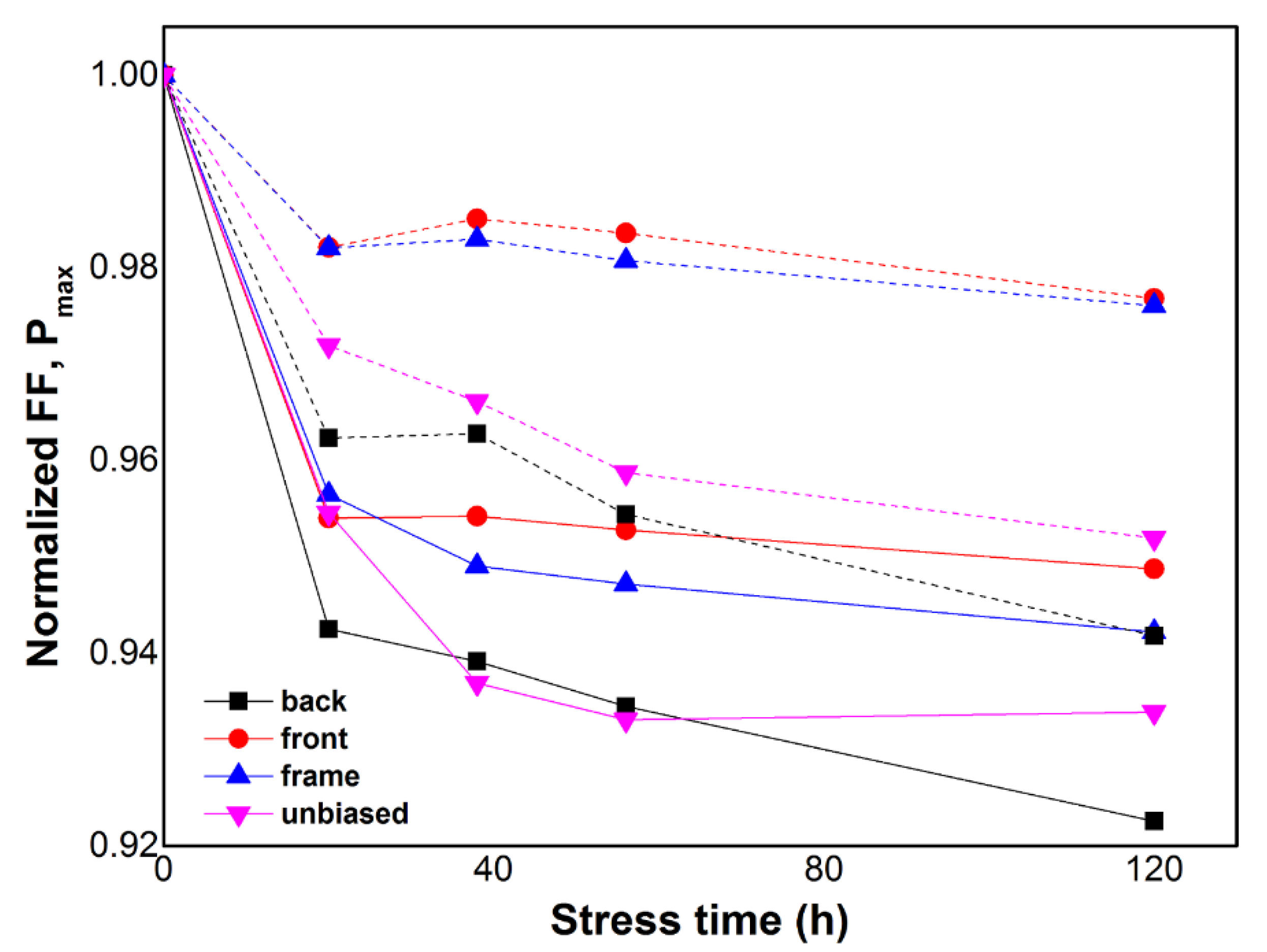
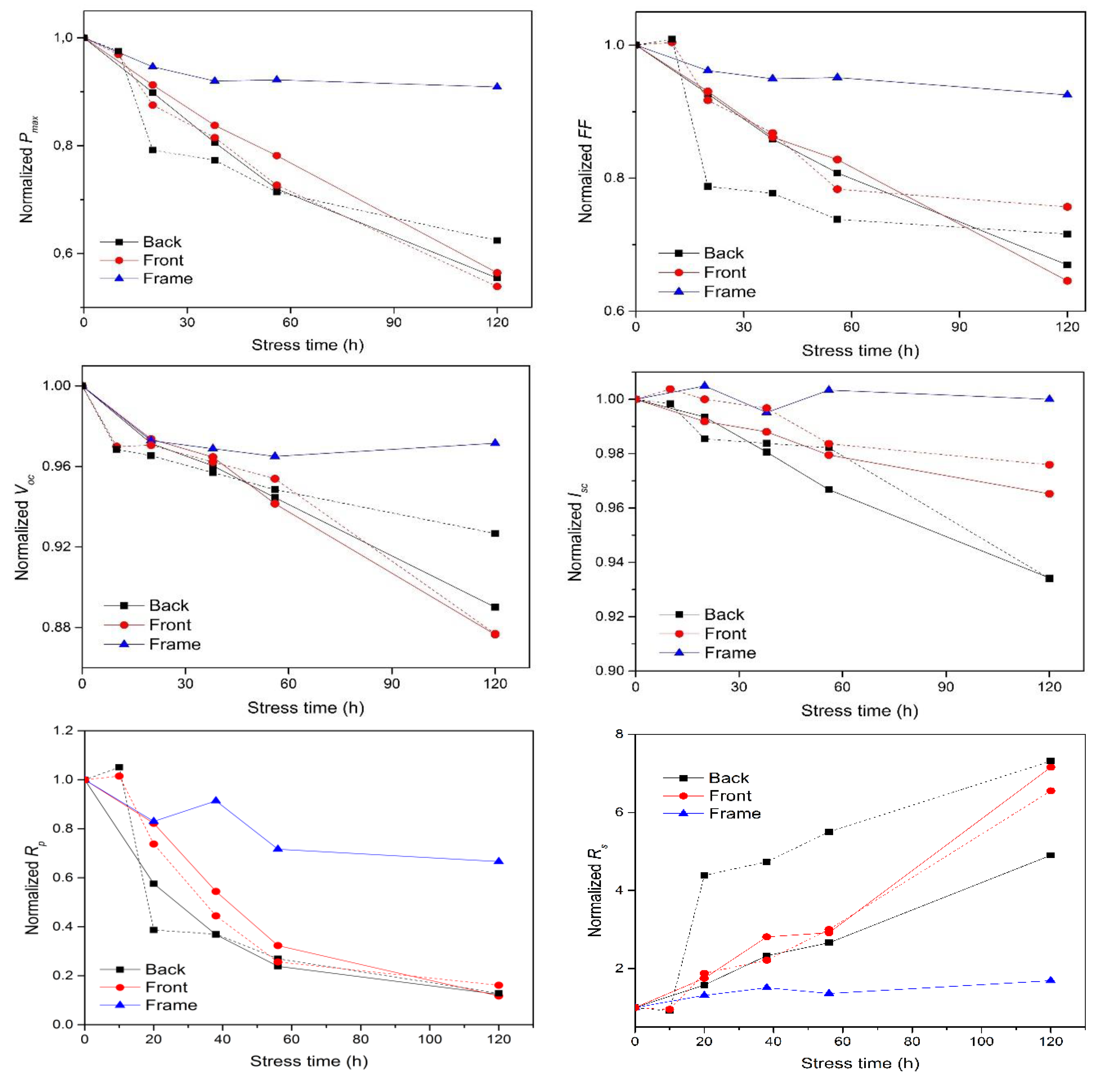
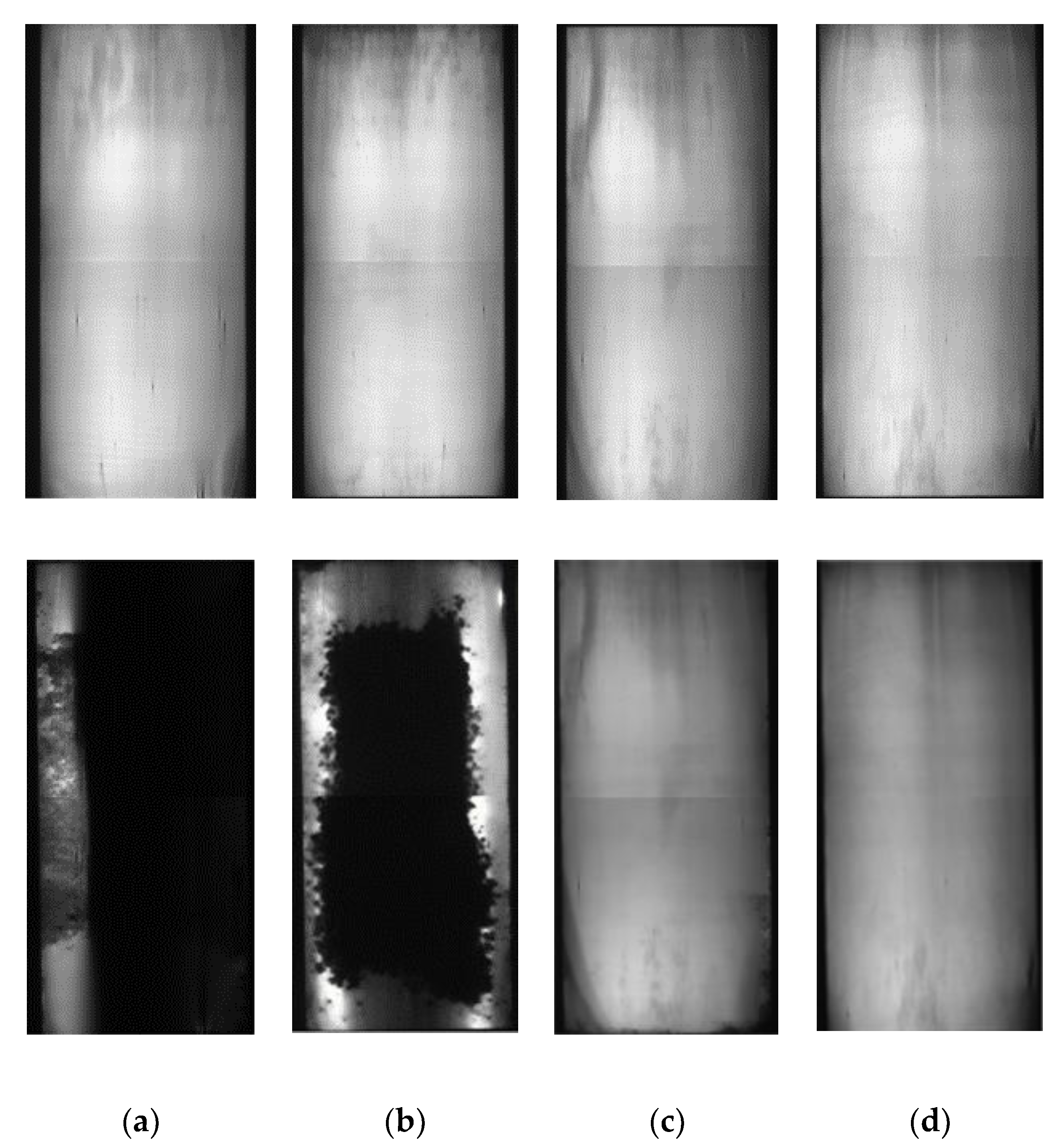
4.1. Degradation
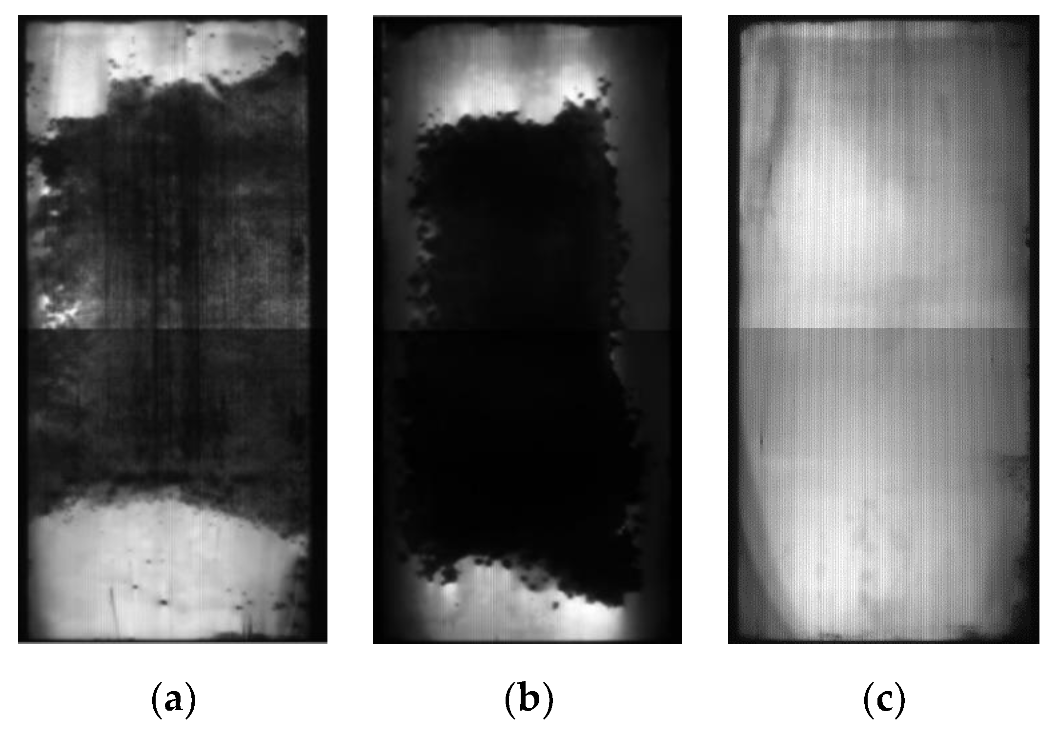
4.2. Recovery
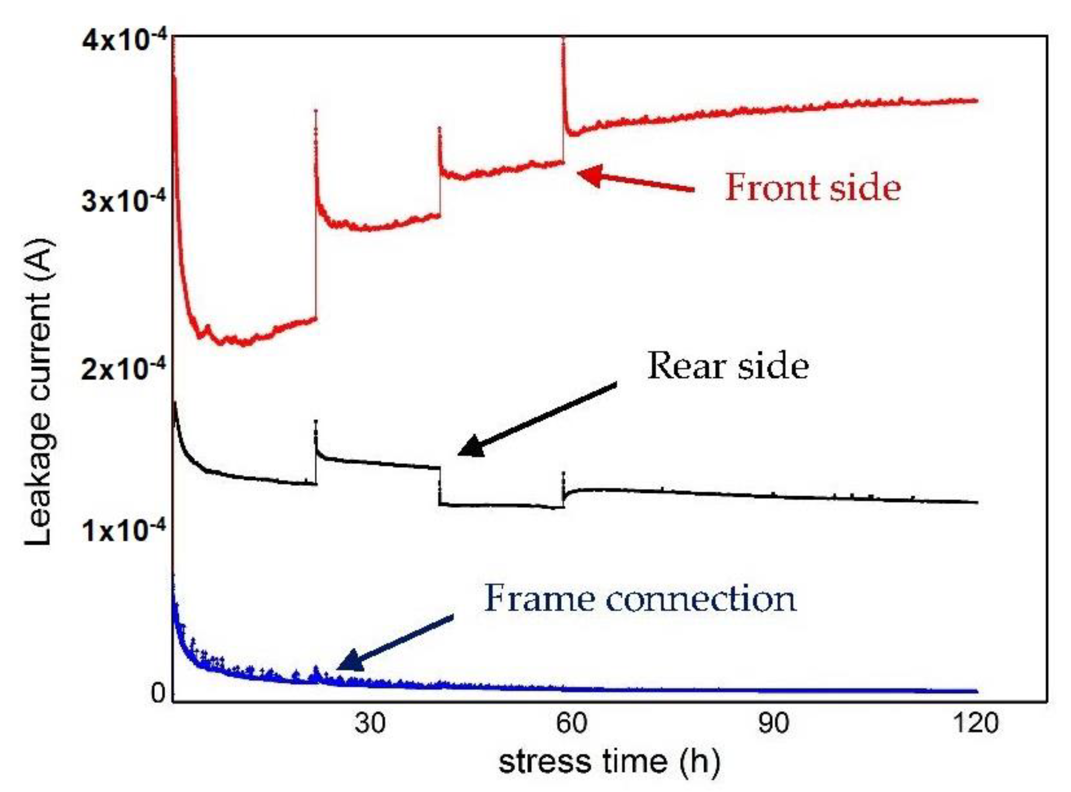
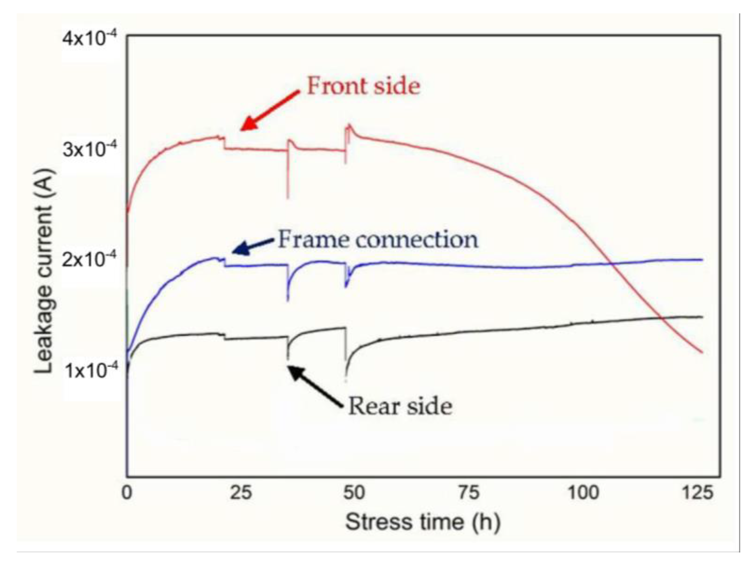
4.3. Leakage Current Analysis
5. Conclusions
Author Contributions
Funding
Conflicts of Interest
References
- Martinez-Moreno, F.; Figueiredo, G.; Lorenzo, E. In-the-field PID related experiences. Sol. Energy Mater. Sol. Cells 2018, 174, 485–493. [Google Scholar] [CrossRef]
- Xiong, Z.; Walsh, T.M.; Aberle, A.G. PV module durability testing under high voltage biased damp heat conditions. Energy Procedia 2011, 8, 384–389. [Google Scholar] [CrossRef]
- Hacke, P.; Smith, R.; Terwilliger, K.; Glick, S.; Jordan, D.; Johnston, S.; Kemp, M.; Kurtz, S. Acceleration factor determination for potential-induced degradation in crystalline silicon PV modules. In Proceedings of the 2013 IEEE International Reliability Physics Symposium (IRPS), Anaheim, CA, USA, 14–18 April 2013. [Google Scholar]
- Nagel, H.; Metz, A.; Wangemann, K. Crystalline Si solar cells and modules featuring excellent stability against potential-induced degradation. In Proceedings of the 26th European Photovoltaic Solar Energy Conference and Exhibition, Hamburg, Germany, 5–9 September 2011. [Google Scholar]
- Islam, M.A.; Hasanuzzaman, M.; Rahim, N.A. A comparative investigation on in-situ and laboratory standard test of the potential induced degradation of crystalline silicon photovoltaic modules. Renew. Energy 2018, 127, 102–113. [Google Scholar] [CrossRef]
- Lechner, P.; Sanchez, D.; Geyer, D.; Mohring, H.-D. Estimation of time to PID-failure by characterisation of module leakage currents. In Proceedings of the 27th European Photovoltaic Solar Energy Conference and Exhibition, Frankfurt, Germany, 24–28 September 2012. [Google Scholar]
- Oh, J.; Bowden, S.; TamizhMani, G. Potential-induced degradation (PID): Incomplete recovery of shunt resistance and quantum efficiency losses. IEEE J. Photovolt. 2015, 5, 1540–1548. [Google Scholar] [CrossRef]
- Goranti, S.; TamizhMani, G. Potential induced degradation (PID) study on accelerated stress tested PV modules. In Proceedings of the 2012 38th IEEE Photovoltaic Specialists Conference, Austin, TX, USA, 3–8 June 2012. [Google Scholar]
- Hara, K.; Ichinose, H.; Murakami, T.N.; Masuda, A. Crystalline Si photovoltaic modules based on TiO 2-coated cover glass against potential-induced degradation. RSC Adv. 2014, 4, 44291–44295. [Google Scholar] [CrossRef]
- Pingel, S.; Frank, O.; Winkler, M.; Daryan, S.; Geipel, T.; Hoehne, H.; Berghold, J. Potential induced degradation of solar cells and panels. In Proceedings of the 2010 35th IEEE Photovoltaic Specialists Conference (PVSC), Honolulu, HI, USA, 20–25 June 2010. [Google Scholar]
- Lausch, D.; Naumann, V.; Breitenstein, O.; Bauer, J.; Graff, A.; Bagdahn, J.; Hagendorf, C. Potential-induced degradation (PID): Introduction of a novel test approach and explanation of increased depletion region recombination. IEEE J. Photovolt. 2014, 4, 834–840. [Google Scholar] [CrossRef]
- Naumann, V.; Lausch, D.; Graff, A.; Werner, M.; Swatek, S.; Bauer, J.; Hähnel, A.; Breitenstein, O.; Großer, S.; Bagdahn, J.; et al. The role of stacking faults for the formation of shunts during potential-induced degradation of crystalline Si solar cells. Phys. Status Solidi RRL Rapid Res. Lett. 2013, 7, 315–318. [Google Scholar] [CrossRef]
- Luo, W.; Khoo, Y.S.; Hacke, P.; Naumann, V.; Lausch, D.; Harvey, S.P.; Singh, J.P.; Chai, J.; Wang, Y.; Aberleae, A.G.; et al. Potential-induced degradation in photovoltaic modules: A critical review. Energy Environ. Sci. 2017, 10, 43–68. [Google Scholar] [CrossRef]
- Fjällström, V. Potential-Induced Degradation of CuIn1−x Gax Se2Thin Film Solar Cells. IEEE J. Photovolt. 2013, 3, 1090–1094. [Google Scholar] [CrossRef]
- Hacke, P.; Smith, R.; Terwilliger, K.; Glick, S.; Pankow, J.; Kloss, M.; Kurtz, S. System voltage potential-induced degradation mechanisms in PV modules and methods for test. In Proceedings of the 2011 37th IEEE Photovoltaic Specialists Conference (PVSC), Seattle, WA, USA, 19–24 June 2011. [Google Scholar]
- Voswinckel, S.; Wesselak, V.; Fokuhl, E.; Schmidt, C.; Watzlawik, K. Dos and don’ts of leakage current measurement. In Proceedings of the 31th European Solar Energy Conference and Exhibition, Hamburg, Germany, 14–18 September 2015. [Google Scholar]
- Manz, P.; Wesselak, V.; Voswinckel, S.; Trautmann, B.; Fokuhl, E.; Schmidt, C. Leakage current pathways and magnitudes in correlation to PID of CIGS thin film modules. In Proceedings of the 29th European Solar Energy Conference and Exhibition, Amsterdam, The Netherlands, 22–26 September 2014. [Google Scholar]
- Colli, A. The role of sodium in photovoltaic devices under high voltage stress: A holistic approach to understand unsolved aspects. Renew. Energy 2013, 60, 162–168. [Google Scholar] [CrossRef]
- Schroeder, D.J.; Rockett, A.A. Electronic effects of sodium in epitaxial CuIn1−x Gax Se2. J. Appl. Phys. 1997, 82, 4982–4985. [Google Scholar] [CrossRef]
- Dhere, N.G.; Shiradkar, S.N.; Schneller, E. Evolution of Leakage Current Paths in MC-Si PV Modules From Leading Manufacturers Undergoing High-Voltage Bias Testing. IEEE J. Photovolt. 2014, 4, 654–658. [Google Scholar] [CrossRef]
- Naumanna, V.; Lauscha, D.; Hähnelb, A.; Bauerb, J.; Breitensteinb, O.; Graff, A.; Werner, M.; Swatek, S.; Großer, S.; Bagdahn, J.; et al. Explanation of potential-induced degradation of the shunting type by Na decoration of stacking faults in Si solar cells. Sol. Energy Mater. Sol. Cells 2014, 120, 383–389. [Google Scholar] [CrossRef]
- Yamaguchi, S.; Jonai, S.; Hara, K.; Komaki, H.; Shimizu-Kamikawa, Y.; Shibata, H.; Niki, S.; Kawakami, Y.; Masuda, A. Potential-induced degradation of Cu (In, Ga) Se2 photovoltaic modules. Jpn. J. Appl. Phys. 2015, 54, 08KC13. [Google Scholar] [CrossRef]
- Spertino, F.; Sumaili, J.; Andrei, H.; Chicco, G. PV Module Parameter Characterization from the Transient Charge of an External Capacitor. IEEE J. Photovolt. 2013, 3, 1325–1333. [Google Scholar] [CrossRef]
- Carullo, A.; Castellana, A.; Vallan, A.; Ciocia, A.; Spertino, F. Uncertainty issues in the experimental assessment of degradation rate of power ratings in photovoltaic modules. Measurement 2017, 111, 432–440. [Google Scholar] [CrossRef]
- Spertino, F.; Ahmad, J.; Ciocia, A.; di Leo, P.; Murtaza, A.F.; Chiaberge, M. Capacitor charging method for I–V curve tracer and MPPT in photovoltaic systems. Sol. Energy 2015, 119, 461–473. [Google Scholar] [CrossRef]
- Ciocia, A.; Carullo, A.; di Leo, P.; Malgaroli, G.; Spertino, F. Realization and Use of an IR Camera for Laboratory and On-field Electroluminescence Inspections of Silicon Photovoltaic Modules. In Proceedings of the 2019 IEEE 46th Photovoltaic Specialist Conference (PVSC), Chicago, IL, USA, 16–21 July 2019. in press. [Google Scholar]
- Fuyuki, T.; Kondo, H.; Yamazaki, T.; Takahashi, Y.; Uraoka, Y. Photographic surveying of minority carrier diffusion length in polycrystalline silicon solar cells by electroluminescence. Appl. Phys. Lett. 2005, 86. [Google Scholar] [CrossRef]
- Lavrenko, T.; Runai, F.R.; Wang, Y.; Teukam, M.; Walter, T.; Hahn, T.; Pistor, P. Advanced luminescence imaging of cigs solar cells. In Proceedings of the 27th European Photovoltaic Solar Energy Conference and Exhibition, Frankfurt, Germany, 24–28 September 2012. [Google Scholar]
- Spertino, F.; Ahmad, J.; Ciocia, A.; di Leo, P. Techniques and Experimental Results for Performance Analysis of Photovoltaic Modules Installed in Buildings. Energy Procedia 2017, 111, 944–953. [Google Scholar] [CrossRef]
- IEC 60904–9. Photovoltaic Devices - Part 9: Solar Simulator Performance Requirements; International Organization for Standardization, ISO Central Secretariat: Geneva, Switzerland, 2007. [Google Scholar]
- BERGER Lichttechnik, Datasheet of Solar Simulation Device “SS8”. Available online: https://www.bergerlichttechnik.de/wp-content/uploads/2018/07/berger_PSS_8_rev417.pdf (accessed on 6 November 2019).
- Lee, D.-W.; Cho, W.-J.; Song, J.-K.; Kwon, O.-Y.; Lee, W.-H.; Park, C.-K.; Park, K.-E.; Lee, H.; Kim, Y.-N. Failure analysis of Cu (In, Ga) Se2 photovoltaic modules: Degradation mechanism of Cu (In, Ga) Se2 solar cells under harsh environmental conditions. Prog. Photovolt. Res. Appl. 2014, 23, 829–837. [Google Scholar] [CrossRef]
- Tosun, B.S.; Feist, R.K.; Gunawan, A.; Mkhoyan, K.A.; Campbell, S.A.; Aydil, E.S. Improving the damp-heat stability of copper indium gallium diselenide solar cells with a semicrystalline tin dioxide overlayer. Sol. Energy Mater. Sol. Cells 2012, 101, 270–276. [Google Scholar] [CrossRef]
- Deline, C.; Stokes, A.; Silverman, T.J.; Rummel, S.; Jordan, D.; Kurtz, S. Electrical bias as an alternate method for reproducible measurement of copper indium gallium diselenide (CIGS) photovoltaic modules. In Reliability of Photovoltaic Cells, Modules, Components, and Systems V; International Society for Optics and Photonics: San Diego, CA, USA, 2012; Volume 8472. [Google Scholar]
- Kobayashi, T.; Yamaguchi, H.; Nakada, T. Effects of combined heat and light soaking on device performance of Cu (In, Ga) Se2 solar cells with ZnS (O, OH) buffer layer. Prog. Photovolt. Res. Appl. 2013, 22, 115–121. [Google Scholar] [CrossRef]
- Dunn, L.; Gostein, M. Light soaking measurements of commercially available CIGS PV modules. In Proceedings of the 2012 38th IEEE Photovoltaic Specialists Conference (PVSC), Austin, TX, USA, 3–8 June 2012. [Google Scholar]
- Helbig, A.; Kirchartz, T.; Schaeffler, R.; Werner, J.H.; Rau, U. Quantitative electroluminescence analysis of resistive losses in Cu (In, Ga) Se2 thin-film modules. Sol. Energy Mater. Sol. Cells 2010, 94, 979–984. [Google Scholar] [CrossRef]
- Voswinckel, S.; Wesselak, V.; Münter, S.; Gerstenberg, L. Correlation of Leakage Current Pathways and Potential Induced Degradation of CIGS Thin Film Solar Modules. In Proceedings of the ISES Solar World Conference 2017 and the IEA SHC Solar Heating and Cooling Conference for Buildings and Industry 2017, Abu Dhabi, UAE, 29 October–2 November 2017. [Google Scholar]


| Parameter | After the PID Test (Before Recovery) | After the Recovery Test | ||||
|---|---|---|---|---|---|---|
| Back | Front | Frame | Back | Front | Frame | |
| Pmax [%] | 0.55 | 0.56 | 0.91 | 0.64 | 0.75 | 0.89 |
| FF [%] | 0.66 | 0.64 | 0.92 | 0.68 | 0.75 | 0.92 |
| Isc [%] | 0.93 | 0.96 | 1.00 | 0.97 | 0.99 | 1.00 |
| Voc [%] | 0.89 | 0.87 | 0.97 | 0.96 | 0.96 | 0.96 |
© 2020 by the authors. Licensee MDPI, Basel, Switzerland. This article is an open access article distributed under the terms and conditions of the Creative Commons Attribution (CC BY) license (http://creativecommons.org/licenses/by/4.0/).
Share and Cite
Boulhidja, S.; Mellit, A.; Voswinckel, S.; Lughi, V.; Ciocia, A.; Spertino, F.; Massi Pavan, A. Experimental Evidence of PID Effect on CIGS Photovoltaic Modules. Energies 2020, 13, 537. https://doi.org/10.3390/en13030537
Boulhidja S, Mellit A, Voswinckel S, Lughi V, Ciocia A, Spertino F, Massi Pavan A. Experimental Evidence of PID Effect on CIGS Photovoltaic Modules. Energies. 2020; 13(3):537. https://doi.org/10.3390/en13030537
Chicago/Turabian StyleBoulhidja, Sofiane, Adel Mellit, Sebastian Voswinckel, Vanni Lughi, Alessandro Ciocia, Filippo Spertino, and Alessandro Massi Pavan. 2020. "Experimental Evidence of PID Effect on CIGS Photovoltaic Modules" Energies 13, no. 3: 537. https://doi.org/10.3390/en13030537
APA StyleBoulhidja, S., Mellit, A., Voswinckel, S., Lughi, V., Ciocia, A., Spertino, F., & Massi Pavan, A. (2020). Experimental Evidence of PID Effect on CIGS Photovoltaic Modules. Energies, 13(3), 537. https://doi.org/10.3390/en13030537