Abstract
With the unceasing advancement of wide-bandgap (WBG) semiconductor technology, the minimal reverse-recovery charge Qrr and other more powerful natures of WBG transistors enable totem-pole bridgeless power factor correction to become a dominant solution for energy storage systems (ESS). This paper focuses on the design and implementation of a control structure for a totem-pole boost PFC with newfangled enhancement-mode gallium nitride field-effect transistors (eGaN FETs), not only to simplify the control implementation but also to achieve high power quality and efficiency. The converter is designed to convert a 90–264-VAC input to a 385-VDC output for a 2.6-kW output power. Lastly, to validate the methodology, an experimental prototype is characterized and fabricated. The uttermost efficiency at 230 VAC reaches 99.14%. The lowest total harmonic distortion in the current (ITHD) at high line condition (230 V) attains 1.52% while the power factor gains 0.9985.
1. Introduction
The grid-tied energy storage system has been one of the most prevailing technological approaches for better harnessing the power generated from “clean” and “green” energy of natural resources, reducing carbon footprints, and providing resiliency to the grid [1,2,3,4,5,6,7,8]. The system can accumulate excess energy into battery packs and feed the stored energy from battery packs back into the utility grid whenever needed by handling power converters. The change in the electric power from a form to another form of DC/DC, DC/AC and AC/DC converters occurs while the reliability, flexibility, stability, efficiency and power quality ought to be still secured [3,4,9,10]. Of all AC/DC converters, the totem-pole boost-type power factor correction (PFC) rectifier has been a promising candidate for ESS applications thanks to superior benefits of bidirectional energy flow capability, high flexibility in control and the least device number [11,12]. Accordingly, as described in Figure 1, an interface with the totem-pole boost-type PFC rectifier is able to construct a bidirectional interconnection of ESS and the grid, thereby taking advantage of the photovoltaic panels and wind turbines as well as enhancing the performance of the entire system [13].
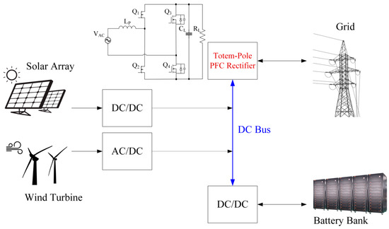
Figure 1.
The totem-pole power factor correction (PFC) rectifier in energy storage systems.
Owing to slow body diode reverse-recovery charge, the typical super junction metal-oxide-semiconductor field-effect transistor (MOSFET)-based totem-pole bridgeless PFC has been restricted to critical-conduction mode operation (CRM) [14,15,16,17]. Even though operating in CRM with a soft-switching method can achieve valley/zero-voltage-switching or zero-current-switching, it is unappealing for higher power applications due to high zero-current-detection subcircuit cost, high EMI noise and high input current ripple. By exploiting more advanced figure-of-merits (FOM) of fast switching WBG power electronic devices such as SiC MOSFETs and GaN FETs to substitute the Si power semiconductors, the WBG device-based totem-pole bridgeless PFC rectifier has become practical for continuous conduction mode operation and improved the power density for the system [11,18,19,20,21,22,23,24,25,26,27,28]. One of the modified versions of the totem-pole bridgeless PFC is implemented with a full-bridge configuration in synchronous rectification mode, comprising active H-bridge switches (Q1, Q2, Q3 and Q4), which reduces the power dissipation when compared to the equivalent diodes [25,28]. These four active switches constructing two switching legs perform voltage step-up function and line rectification. As shown in Figure 1, two fast 650 V eGaN FETs, which are opted for this work, play the same role as boost converters, whereas two low resistance Silicon MOSFETs are placed to exterminate conducting diodes. Correspondingly, the power conduction path embraces one fast switch and one slow switch without related diode drop to ameliorate the efficiency.
Similar to most of the bridgeless topologies, it is evident that an inherent challenge of the totem-pole boost PFC is the conspicuous common-mode (CM) noises, especially a pounding current spike at the zero-crossing interval of AC voltage, which significantly aggravates the current line quality, such as total harmonic distortion (THD) and power factor (PF) [29,30,31,32]. The high current harmonic distortion would destructively affect the grid as well as the other electrical equipment connecting to the grid, while the low power factor would provoke the energy extravagance. As is known, the Si MOSFET is modeled as an ideal switch with a body diode and a parasitic capacitor. Aside from the cause of the abrupt alteration in the duty cycle, the zero-crossing distortion rooted by the poor reverse recovery characteristic of the body diode and sudden discharge of the parasitic output capacitance of the slow speed leg upper switch Q3 (from positive to negative half-cycle transition point) or lower switch Q4 (from negative to positive half-cycle transition point) when the corresponding fast leg active switch turns on. For example, during the swap from negative to positive mains half-line cycle of the input voltage, GaN FET Q2 becomes the active switch in the high-frequency leg. Since input voltage is approximately zero, in order to output voltage reaches 385 V, Q2 has the widest duty while Q4 was blocking 385 V during the negative half of the AC line cycle. For this reason, when Q2 turns on, the charge stored in the parasitic output capacitance of Q4 will incur a positive current spike on the input inductor. To gradually discharge the parasitic output capacitance of the slow-speed leg Si MOSFET, the soft-start technique with multiple gate pulses of increasing small duty ratio is applied at zero-crossing area [33].
In order to circumvent the requirements on power performance and obstacles surrounding the bidirectional inductor current, lacking a bridge rectifier and the function interchange among switches, a new control structure is proposed with the harmony in both firmware and hardware to expedite the control algorithm and implementation. This paper is organized into five sections. Section 2 gives a proposed control architecture of the individual blocks over the totem-pole PFC converter topology. In Section 3, firmware considerations on the control strategy of the converter are presented in detail. Section 4 shows the experimental results, encompassing the measured waveforms, converter efficiency, PF and THD in the current under different conditions. Finally, conclusions and remarks are drawn in Section 5.
2. Proposed Control Structure
2.1. Block Diagram
The block diagram of the proposed control system for the totem-pole PFC rectifier, which is displayed in Figure 2, consists of major parts: power stage and sensing circuit, digital signal processor (DSP) controller block and auxiliary logic circuit. Each block is described in more detail in the following sections. Four signals, including the line voltage sensing signal, the neutral voltage sensing signal, the inductor current sensing signal and the output voltage sensing signal, are acquired from the power stage circuit by the signal conditioning and sensing circuits to feed to the digital control block.
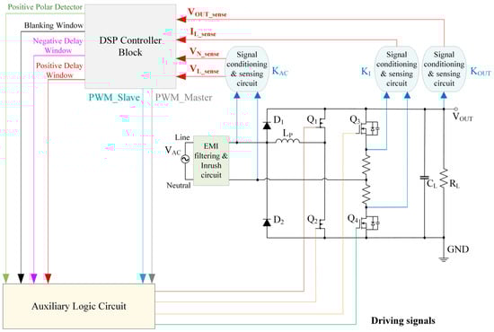
Figure 2.
Simplified block diagram of the proposed structure.
KAC, KI and KOUT denote the gain of the mains voltage sensing circuit, the gain of the current sensing circuit, and the gain of the output voltage sensing circuit, respectively. Because the measurement range of analog-to-digital (ADC) pins within DSP is from 0 to 3.3 V, the sensing signals are scaled in order not to be greater than the maximum value of 2.5 V. For this tolerance purpose, KAC, KI and KOUT should be limited by
where IRMS_MAX is the maximum root-mean-square value of the input current
where IRMS_MAX is the maximum root-mean-square value of the input current
2.2. Power Stage and Sensing Circuit
2.2.1. Power Stage
The power stage of the totem-pole bridgeless PFC rectifier contains a pair of GaN FETs (Q1, Q2) that switches at PWM frequency and a pair of regular MOSFETs (Q3, Q4) that operates at line frequency. Apart from EMI filtering and inrush circuit, two diodes (D1, D2) are added in front of the PFC choke to cope with the huge current for the load capacitance pre-charge. The topology operates in two modes depending on the polarity of the AC voltage, where each fast-speed leg switch must perform either master or slave mission as displayed schematically in Figure 3.
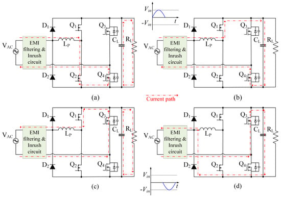
Figure 3.
Current flows during positive and negative AC half cycles: (a) positive AC half-cycles from 0 to DTs; (b) positive AC half-cycles from DTs to Ts; (c) negative AC half-cycles from 0 to DTs; (d) negative AC half-cycles from DTs to Ts.
During the positive semi-period of the input voltage, Q4 is in ON–state and Q3 is in OFF–state: upper fast-speed leg switch Q1, lower fast-speed leg switch Q2 and power inductor LP form a boost DC/DC stage where Q2 acts as a master switch and Q1 acts as slave switch. The operating states when the input AC voltage is positive are illustrated in Figure 3a,b. When the main switch Q2 is ON with t = (0, DTs) (where D is the duty cycle and Ts is the switching period), the current flows from the choke LP to Q4 through Q2 and back to neutral. The load is charged by the output capacitor at the same time in this half-line cycle. When Q2 is open and Q1 is closed with t = (DTs, Ts), the current flows via Q1, then via the output capacitor and load, and back to neutral through Q4. The ground of the output side is tied to neutral potential as Q4 is conducting all the time in a positive half-line cycle. Another complete switching cycle repeats when Q2 switches on again by the gate-to-source voltage of the driver circuit. Similarly, during the negative half-line cycle, Q3 is in ON–state and Q4 is in OFF–state: the operation in the negative half-line cycle is analogous except the role of the upper and lower switches are exchanged. Q1 turns out to be the master switch, and Q2 becomes the slave switch. Figure 3c,d depict the operation principle when the input AC voltage is negative. Reliance on two major operating modes, together with optimizing the performance, a new control signal sequence is depicted and explained in Section 2.4.
2.2.2. Signal Conditioning and Sensing Circuit
Referring to Figure 4, the signal conditioning and sensing circuit is the interface of the power stage and control stage. For the sake of controller design, the system uses four sensing circuitries and filters to sense the vital signals, namely input current IL_sense, bus voltage VOUT_sense, input voltage Neutral VN_sense and input voltage line VL_sense.
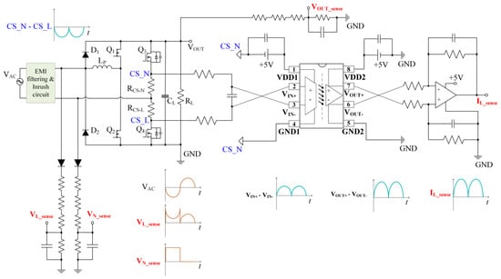
Figure 4.
Sensing circuit of the proposed design.
Similar to most members belonging to the bridgeless PFC family, the current of totem-pole PFC rectifier also withstands a fluctuating input line in regard to the output voltage ground and a continuous shift of direction due to the inactivity of a boost converter branch in either cycle, an isolation methodology is thus a must. In addition, the totem-pole PFC controller needs a rectified current reference signal rather than the AC input current to realize PFC. To accomplish the requirement, two straightforward shunt resistors RCS_N and RCS_L, are placed between the lower switch of slow speed phase leg Q4 and the neutral terminal of the AC grid, upper switch Q3 and neutral terminal correspondingly.
An isolated sensing solution is applied with an isolation amplifier and an operational amplifier, which are assembled in series after the current sensing resistors. The +5 V supply voltage for input side VDD1 in respect of CS_N point is transported from the output of a low dropout voltage regulator IC, which also drives the upper switch Q3. The input side ground GND1 of the isolation amplifier is referred to as the CS_N point, while the output side ground GND2 is linked to the ground of the power stage. It can be observed from Figure 4 that the waveform of IL_sense with desired gain and rectified positive shape is achieved as the output of the differential amplifier. The gain of the current sensing circuitry is able to be derived as
RCS, GIso and GOA are the expressions of the resistance of the current sensing resistor, the gain of the isolation amplifier and the gain of the op-amp, respectively. The inductor current obtains the highest value when the difference in the positive input voltage and the negative input voltage reaches the maximum value, which is effortlessly inferred from the component datasheet. The value of current sensing resistors RCS_N and RCS_L should be selected depending mainly on the estimated division between the maximum value in the differential input voltage of the isolation amplifier and the peak value of the root-mean-square value of the input current.
Moreover, in this design, the designated shunt resistors are non-inductive resistors in an attempt of minimizing the di/dt slew rate induced voltage spikes, which may have a detrimental impact on the operation. In the aspect of sensing the input voltage, a low-frequency transformer is regularly employed. Nevertheless, the transformer is costly, bulky and occupies a large area of the circuit, which makes it incompatible with the high efficiency-oriented application. The higher linearity optical coupler with a wide operating range is a common solution for voltage sensing as well. However, in comparison with the voltage dividers, the optical coupler is much more complicated. In this paper, the line AC voltage and neutral AC voltage are sensed separately by the voltage divider and then filtered to eliminate high-frequency interference noises by a low-pass filter with waveforms as displayed in Figure 4. Hence, the targeted sinusoidal VAC is obtained through the rectification function in the DSP control block. The feedback circuit of DC output voltage is also implemented by a voltage divider in combination with an RC network for simplicity.
2.3. DSP Control Block
The functional block diagram of the controller inside the DSP is introduced in Figure 5. In this paper, the controller is implemented by using digital control with 60 MHz Texas Instrument core-TMS320F28035. It is necessary to use four input signals IL_sense, VOUT_sense, VN_sense and VL_sense for compensators as well as different functions. These sensed signals are converted to digital by using 12-bit ADC modules for sampling and conversion process from the DSP. Moreover, then, based on the control method described in Section 3, the duties for the master switch and the slave switch can be determined and implemented through enhanced pulse width modulation (EPWM) modules. In this way, by using the auxiliary control circuit, the accurate gating signals are delivered for controlling all switches at any operating condition by the logic control circuit. It is worth noting that the grid voltage VAC is measured by sensing the VN_sense and VL_sense independently; thus, the VAC_DSP which is used for calculation in DSP should be derived as:
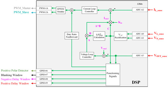
Figure 5.
Functional block diagram of the controller within the digital signal processor (DSP).
When the converter operates in the positive AC semicycle, the VAC_DSP is equal to the difference of VL_sense − VN_sense while the VAC_DSP is equal to the difference of Vn_sense − VL_sense during the negative half-line cycle.
Figure 5 also shows that the totem-pole PFC controller is composed of two control loops: the voltage control loop is a low-frequency outer loop which regulates the output voltage of the boost power stage to be equal to the desired reference value, while the current control loop is a high-frequency inner loop whose target is to make certain the input current shape to be a replica of the AC voltage shape. In terms of the voltage control loop, VOUT_sense is subtracted from the reference output voltage Vcmd. The resulting difference signal Vcmd − VOUT_sense is then fed into the voltage loop controller. The bandwidth of the voltage loop must be far less than 120 Hz to sufficiently attenuate the second harmonic of the output voltage. As for the current loop, IL_sense is subtracted from the current command Icmd. The resulting difference signal (Icmd − IL_sense) is then fed into the current loop type II controller, whose output is sent to the EPWM module. However, only the current loop controller cannot make the power qualities meet the requirements. An advanced technique, i.e., duty-ratio feedforward from [34], is combined with this duty cycle to create the PWM_Master and PWM_Slave in a suitable way. A deadtime is accompanied between these two EPWMs in the middle of switching events to be immune to shoot-through conditions while the master and slave switch fleetingly turn off. Moreover, it is important to note that the other four functioning signals, positive polar detector, blanking window, negative delay window and positive delay window, are fashioned for different purposes, which is stated more visibly in the following auxiliary circuit.
2.4. Auxiliary Logic Circuit
The establishment of the auxiliary control logic circuit is based on the idea of exporting the turn-on and turn-off sequence of four switches Q1, Q2, Q3 and Q4, in a smooth and simple way. As shown in Figure 6, a straightforward signal sequence (on the left-hand side) and an auxiliary control logic circuit (on the right-hand side) are further elaborated to generate the expected signals for all switches.
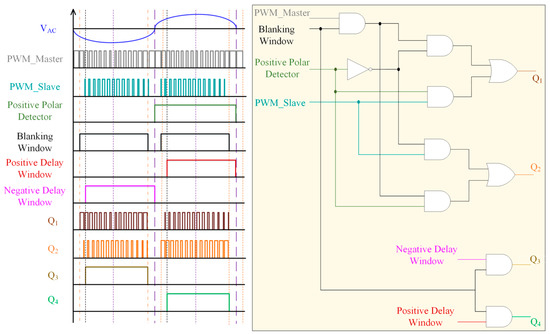
Figure 6.
Key signal sequence (left) and auxiliary logic circuit (right) of the proposed control structure.
There are six input signals of the control subcircuit sent from the DSP controller and four targeted output signals transmitted to the gating driver of switches. Among them, the duty cycle for the main switch PWM_Master and the duty cycle of the synchronous-rectifier switch PWM_Slave is directly routed from the output of the controller. One of the four remaining functioning-signals is a positive polar detector formed from sensing the input grid voltage VAC to decide which switches work according to the distinct operating mode of the totem-pole PFC rectifier. The output signal of the positive polar detector is HIGH when the grid voltage goes positive. On the other hand, the output signal of the positive polar detector goes LOW as the grid voltage is negative. A NOT logic gate is used to invert the positive polar detector signal in the effort of avoiding the shoot-through of two fast-speed switches at the same time. These signals also have the capability of enabling and disabling AND gates to switch the PWM sequences alternately for each half-line period. Meanwhile, a blanking window is supplemented for safety purposes under abnormal conditions in which all switches are turned off during the commutation intervals at the boundaries of positive and negative half-line cycles. For the reason of evading unwanted issues instigated by the crossover current spikes, the negative delay window and positive delay window are proposed to insert the delay time between turn on moments of the fast speed leg and slow speed leg. More specifically, the negative delay window and positive delay window are realized by turning on Q3/Q4 after Q1/Q2 experiences a turn-on in either semicycle such that the slow-speed leg switches can completely reverse recover whereby the drive gating signals for line-frequency-switched devices and high-frequency-switched devices are fulfilled in an optimal way. This course is important since it contributes pointedly to downgrade the current spikes and the ITHD.
3. Firmware Design for the Control Strategy
3.1. Algorithm Flowchart
This prototype totem-pole PFC software is implemented by EPWM interrupt service routine (ISR) of DSP controller, with running all PFC functions, and state machines in the periodical interrupt. In addition to the PFC functions and state machines, initializing the variables and clearing the controller parameters, in the beginning, handled in the main background loop. The control method is designed to form one compact software and can be easily integrated into the DSP controller of the application for easing to use in the industrial environment. The entire PFC control software is implemented in two ISRs. The current loops are executed in the fast interrupt every 15.38 µs, the voltage loop and state machine are executed in the slower interrupt with a 30.76 µs period of execution. The flowchart of the ISR loop is shown in the following Figure 7.
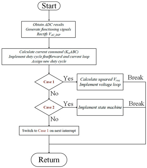
Figure 7.
The principal software flowchart of the proposed control structure.
The flowchart for PFC implementation is explained in more detail below. These critical tasks are assigned in the ISR loop.
- Obtain ADC results: The task aims at acquiring 4 ADC channel values comprising the line voltage sensing signal, the neutral voltage sensing signal, the inductor current sensing signal and the output voltage sensing signal.
- Generate functioning signals: In the hardware design, employing the proper driving signals at the auxiliary logic circuit for controlling GaN switches and MOSFETs results in the need of generating functioning signals such as positive polar detector, blanking window, negative delay window and positive delay window. Accordingly, this task creates these functioning signals based on the ADC results of the line voltage sensing signal, the neutral voltage sensing signal and the output voltage sensing signal as aforesaid in Section 2.3. Software counters are appropriately added to remove glitches or noises influencing these functioning signals adversely. For instance, in case of the positive polar detector signal changes the state from HIGH to LOW, but not at the zero-crossing zone, which enables the counter increment in a row, a threshold is programmed with such a higher value than this counter that the function can clear the improper signal. Otherwise, the controller will behave as if the AC grid swaps to a negative semicycle. Thus an enormous current spike will be produced by being shorted between the ground and output bus, resulting in the damage of the components.
- Rectify Vac_DSP: The task produces the rectified waveform (M-shape waveform) of the AC mains voltage sensing signal to prepare for calculating the current command.
- Calculate current command (ABCKm): The task calculates the current command Icmd where factors are established in corresponding as follows: The notation A is the output of the voltage loop controller whose maximum value and minimum value contain:
Afterward, the notation B, which is the inverse of squared Vrms, is derived to calculate within DSP by:
where is the DSP coefficient of 12-bit ADC. It should be noticed that both A and B are calculated in the previous interrupt service routine. Next, C denotes the AC mains voltage sensing signal:
Moreover, then Km is the multiplier gain, which is specified as a constant designed in advance. To choose the proper Km, some extra steps should be taken. The first action is expressing the current command from Equations (7)–(9):
Simplifying and substituting , the Equation (10) becomes:
Meanwhile, the measured current value is given within DSP by:
Substituting , the Equation (12) becomes:
Following the current control law, the measured current value must be equal to the commanded current value , combining the Equations (12) and (13) with due to the close-to-unity power factor, Km is deducted as:
- Implement Duty-cycle feedforward and current loop: The current loop controller is designed and implemented by DSP to catch improved duty cycles for PWM_Master and PWM_Slave.
- Assign the new duty cycle: After implementing the duty feedforward and current loop controller, the new duty value is available. Afterward, an upper-end limitation is imposed on this updated duty ratio to prevent excessive current and instability when working at a high duty ratio. Therefore, the objective of this task is assigning the novel duty cycle value to assure the duty of EPWMs signals placed on the correct gate driver’s signal pin.
3.2. State Machine
Referring to Figure 8, five specific states of the PFC state machine are described briefly with the state diagram.
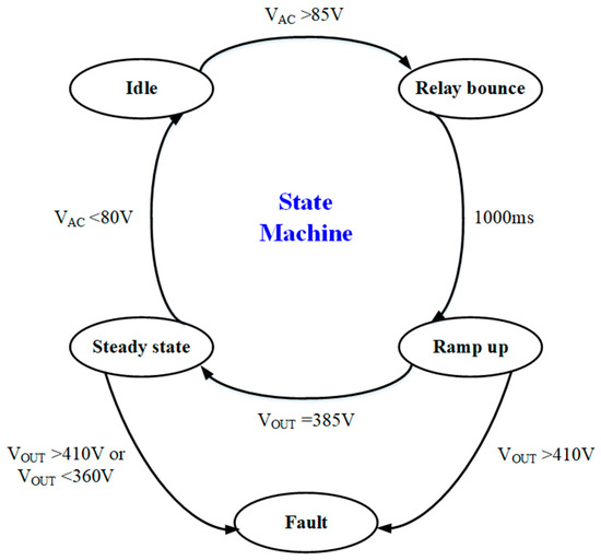
Figure 8.
PFC state diagram running in interrupt service routine (ISR).
- Idle: Inrush current relay is turned off rather than bypassing the inrush current resistor in the beginning. Inrush current relay is turned on (bypass the inrush current resistor) and moving to the next state if VAC is continually higher than 85 V during 100 ms. At the beginning of a start-up, both outputs of the voltage loop and control loop are zero.
- Relay bounce: Checking VAC is still higher than 85 V after the relay bounces. If VAC is stable in a duration of 1000 ms, the controller is enabled.
- Ramp-up: The output voltage value is elevated linearly. The controller forces the output voltage to follow the reference value until the output voltage reaches the demanded value. This leads to protecting the circuit from the excessive starting-up current.
- Steady state: The normal condition of PFC operation and checking of an overvoltage condition.
- Fault: The incidents of fault state concerning the output voltage are determined by being out of range. Once the voltage exceeds more or less than 6% of its nominal value, the controller will activate the overvoltage protection.
4. Experimental Results
To confirm the functionality and to measure the efficiency of the circuit, a pertinent experimental arrangement is formed. Figure 9 depicts a global view of the realized converter, whereas Table 1 tabulates the specification of the prototype. A 2.6 kW totem-pole PFC prototype is built with the standard grid voltage range of 90 to 264 VAC. The control daughter card is attached to the mother power stage board and works as the brain for the whole converter. The needed value for current sense resistors is 10 mOhm for each side of the slow-speed leg to compromise the measurement accuracy and the power dissipation, as mentioned previously. To satisfy the required wattage, four 0.04 Ohm resistors are stacked in parallel. The footprint dimension of the designed circuit is 11.9 cm × 9.6 cm × 5.4 cm.
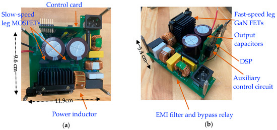
Figure 9.
Perspective of the hardware prototype: (a) bird’s eye view; (b) top side view.

Table 1.
The specification and the parameters of the design.
Figure 10 displays the experimental waveform of the input voltage and the inductor current under the full load condition of the 2.6 kW at 230 VAC and the 1 kW at 115 VAC. It can be shown that the inductor current (channel 2) is perfectly sinusoidal and in phase with the input voltage (channel 1) seamlessly.
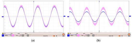
Figure 10.
Experimental waveforms of the totem-pole PFC rectifier running (a) at 230 VAC input and 2.6 kW output load; (b) at 115 VAC input and 1 kW output load (for both left and right figures: VAC 100 V/division, channel 1– IL 5 A/division, channel 2. Timebase 5 ms/division).
In order to reveal dynamic responses of the prototype, a load step from low to high and from high to low load with the output voltage tightly regulated at 385 VDC. Figure 11a–d display the transition conditions of load from 100% to 50%, from 50% to 100%, from 50% to 0%, and from 0% to 50%. The purple curve (channel 1), the hot pink curve (channel 2), the light blue curve (channel 3), and the dark yellow curve (channel 4) demonstrate the AC input voltage, the inductor current, the output current, and the DC link voltage on the output terminal, respectively. The input current hits the new static operation point shortly after a few mains period with a trivial overshoot at first. The bus voltage fully recovers within roughly 395 ms and discloses the maximum deviation of 34 V.
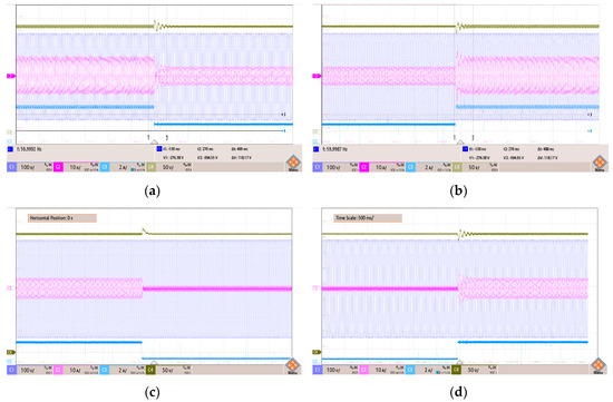
Figure 11.
Measurement result of the transient response (a) from 100 to 50 percent load; (b) from 50 to 100 percent load; (c) from 50 to 0 percent load; (d) from 0 to 50 percent load. (for all figures: VAC 100 V/division, channel 1– IL 10 A/division, channel 2– VOUT 50 V/division, channel 3– IOUT 2 A/division, channel 4. Timebase 500 ms/division).
The prototype of the totem-pole PFC rectifier is also tested under the start-up scheme of the converter at the mains voltage of 90 VAC and 230 VAC with a minimum load of 300 mA, as revealed in Figure 12a,b. The light blue curve (channel 3) shows the DC link voltage on the output, whereas the hot pink curve (channel 2) embodies the inductor current and the purple curve (channel 1) depicts the input voltage, respectively. Referring to these figures, the complete start-up procedure takes approximately 1950 ms. The input AC voltage achieves the start value after several first charging pulses. Subsequently, the input current rises in a linear way until the bus voltage achieves the designed value. As soon as VOUT reaches this point, the state machine turns into the Steady state, and the circuit jumps to the regulation operation. This feature can deal with excessive power dissipation and reduce device stress.
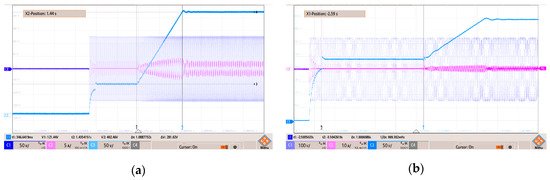
Figure 12.
Start-up waveforms of the totem-pole PFC (a) at 90 VAC with 300 mA load current; (VAC 50 V/division in AC coupling mode, channel 1– IL 5 A/division, channel 2– VOUT 50 V/division, channel 3. Timebase 500 ms/division) (b) at 230 VAC with 300 mA load current (VAC 100 V/division in AC coupling mode, channel 1– IL 10 A/division, channel 2– VOUT 50 V/division, channel 3. Timebase 200 ms/division).
The efficiency curve with relation to the continuous output power at 230 VAC line voltage is shown in Figure 13, where the efficiency achieves 99.14% at nominal high line conditions and maintains over 98.5% for the whole load range.
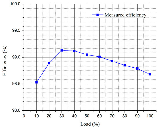
Figure 13.
The efficiency curve with the overall load range of 2.6 kW at high line condition 230 VAC.
The measured PF and ITHD values, which are the major reference for evaluating the power quality performance, are essentially decided by the control methodology and compensation rather than the power stage. Table 2 summarizes the measured PF and THD of the proposed control structure at the minimum and maximum input AC voltage over ten different load levels. The PF and THD measured at maximum line full load are 0.998% and 2.79%, respectively, whereas those at the minimum line are 0.999% and 1.76%, respectively. Meanwhile, Figure 14 shows the power factor at low input voltage 115 VAC (dot-dashed line) and high input voltage 230 VAC (solid line). The power factor higher than 0.99 from 30% load to 100% load.
Table 2.
The measured total harmonic distortion (THD) and power factor (PF) at the line voltage of 90 V and 264 V.
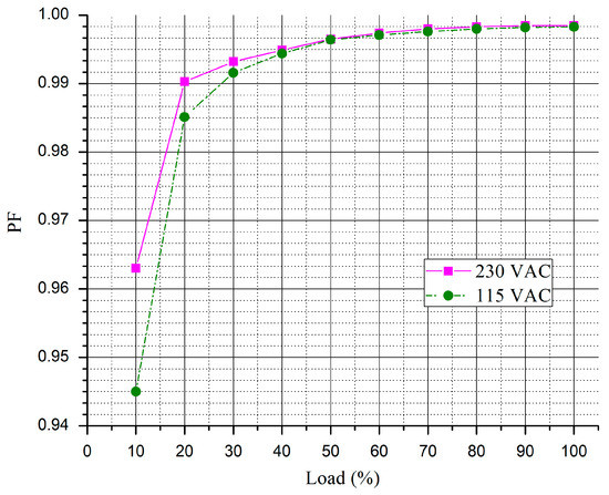
Figure 14.
The measured PF curve with respect to the overall load range at low line 115 VAC and high line 230 VAC.
As illustrated in Figure 15, the ITHD gains further improvement when applying the functioning signals around the zero crossing. The black curve shows the ITHD values with functioning signals applied, while the red curve presents those without functioning signals. Compared to the ITHD of 3.74% under the 230-VAC testing condition of the control strategy without functioning signals, the ITHD with offered functioning signals achieves 1.52% at the mid-range of output power and is always smaller than 3% only except at 10% load condition. As the power level is very low, the input of the amplifier for the current measurement is very small, whereby the sensing current signal has a larger error unmatched with the current reference, leading to a higher ITHD value. Such a figure also shows the current spikes at zero crossings notably disappear when applying the functioning signals.
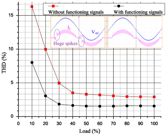
Figure 15.
The measured harmonic distortion in the current (ITHD) and waveform comparisons with both the presence and absence of the functioning signals at the grid voltage zero-crossing zone over the full range of load.
5. Conclusions
The proposed solution was implemented by combining hardware and firmware to optimize the performance of the e-mode GaN-based totem-pole PFC rectifier for grid-connected ESS, no longer only at rated power but also throughout a wide load range. The adopted control structure has the merits of easy implementation, a simple algorithm with a digital controller on the DSP TMS320F28035, which is tough to be accomplished with a more intricate model owing to the obligatory calculation attempt. The analytic and experimental results on a 2.6 kW prototype demonstrated excellent performance where the power factor can be improved to near unity, the efficiency surpasses 99% over the large load range, and the input current total harmonic distortion reduces to 1.52. The control also diminishes the component stress during the soft start-up procedure considerably. The steady-state and dynamic behaviors proceed at a PCB size of 119 mm × 96 mm and a height of 54 mm to justify the prototype’s feasibility as well.
Author Contributions
The author N.-N.D. conceived the control design method, verified with simulation and experiments, debugged the system and wrote the paper. The author B.-S.H. was responsible for investigating the literature resources, layout and hardware consideration. The author T.-T.N. was responsible for building some parts of hardware and software, as well as carrying out the experiments. The authors N.-T.P. and J.-H.W. were responsible for testing the circuit and data acquisition. The authors H.-J.C. and Y.-C.L. supervised the research, provided materials for experiments, and reviewed the paper. All authors have read and agreed to the published version of the manuscript.
Funding
This research received no external funding.
Conflicts of Interest
The authors declare no conflict of interest.
References
- Padmanabhan, N.; Ahmed, M.; Bhattacharya, K. Battery energy storage systems in energy and reserve markets. IEEE Trans. Power Syst. 2019, 35, 215–226. [Google Scholar] [CrossRef]
- Arani, A.K.; Gharehpetian, G.; Abedi, M. Review on energy storage systems control methods in microgrids. Int. J. Electr. Power Energy Syst. 2019, 107, 745–757. [Google Scholar] [CrossRef]
- Hannan, M.; Lipu, M.H.; Ker, P.J.; Begum, R.; Agelidis, V.G.; Blaabjerg, F. Power electronics contribution to renewable energy conversion addressing emission reduction: Applications, issues, and recommendations. Appl. Energy 2019, 251, 113404. [Google Scholar] [CrossRef]
- Vazquez, S.; Lukic, S.M.; Galvan, E.; Franquelo, L.G.; Carrasco, J.M. Energy storage systems for transport and grid applications. IEEE Trans. Ind. Electron. 2010, 57, 3881–3895. [Google Scholar] [CrossRef]
- Xue, F.; Yu, R.; Huang, A.Q. A 98.3% efficient GaN isolated bidirectional DC–DC converter for DC microgrid energy storage system applications. IEEE Trans. Ind. Electron. 2017, 64, 9094–9103. [Google Scholar] [CrossRef]
- Qian, H.; Zhang, J.; Lai, J.-S.; Yu, W. A high-efficiency grid-tie battery energy storage system. IEEE Trans. Power Electron. 2010, 26, 886–896. [Google Scholar] [CrossRef]
- Pahlevani, M.; Eren, S.; Guerrero, J.M.; Jain, P. A hybrid estimator for active/reactive power control of single-phase distributed generation systems with energy storage. IEEE Trans. Power Electron. 2015, 31, 2919–2936. [Google Scholar] [CrossRef]
- Bagawade, S.; Mousavian, H.; Jain, P.; Pahlevani, M. A novel bi-directional AC/DC converter used for Energy Storage Systems (ESSs). In Proceedings of the 2017 IEEE Applied Power Electronics Conference and Exposition (APEC), Tampa, FL, USA, 26–30 March 2017; pp. 459–466. [Google Scholar]
- Kwon, O.; Kim, J.-S.; Kwon, J.-M.; Kwon, B.-H. Bidirectional grid-connected single-power-conversion converter with low-input battery voltage. IEEE Trans. Ind. Electron. 2017, 65, 3136–3144. [Google Scholar] [CrossRef]
- Dragicevic, T.; Meng, L.; Blaabjerg, F.; Li, Y. Control of Power Converters in ac and dc Microgrids. In Wiley Encyclopedia of Electrical and Electronics Engineering; Wiley: Hoboken, NJ, USA, 2019. [Google Scholar]
- Shao, J.; Agrawal, B.; Bathula, V.S.; Mangal, N.; Moxey, G. Analog Based High Efficiency 2 KW Totem Pole PFC Converter Using Surface Mount SIC MOSFET’s. In Proceedings of the PCIM Europe 2018, International Exhibition and Conference for Power Electronics, Intelligent Motion, Renewable Energy and Energy Management. Nuremberg, Germany, 5–7 June 2018; pp. 1–6. [Google Scholar]
- Li, Q.; Andersen, M.A.; Thomsen, O.C. Conduction losses and common mode EMI analysis on bridgeless power factor correction. In Proceedings of the 2009 International Conference on Power Electronics and Drive Systems (PEDS), Taipei, Taiwan, 2–5 November 2009; pp. 1255–1260. [Google Scholar]
- Eren, S.; Pahlevani, M.; Bakhshai, A.; Jain, P. A digital current control technique for grid-connected AC/DC converters used for energy storage systems. IEEE Trans. Power Electron. 2016, 32, 3970–3988. [Google Scholar] [CrossRef]
- Firmansyah, E.; Tomioka, S.; Abe, S.; Shoyama, M.; Ninomiya, T. Totem-Pole Power-Factor-Correction Converter under Critical-Conduction-Mode Interleaved Operation. IEICE Trans. Commun. 2010, 93, 2250–2256. [Google Scholar] [CrossRef]
- Su, B.; Zhang, J.; Lu, Z. Totem-pole boost bridgeless PFC rectifier with simple zero-current detection and full-range ZVS operating at the boundary of DCM/CCM. IEEE Trans. Power Electron. 2011, 26, 427–435. [Google Scholar] [CrossRef]
- Marxgut, C.; Krismer, F.; Bortis, D.; Kolar, J.W. Ultraflat interleaved triangular current mode (TCM) single-phase PFC rectifier. IEEE Trans. Power Electron. 2013, 29, 873–882. [Google Scholar] [CrossRef]
- Huang, L.; Yao, W.; Lu, Z. Interleaved totem-pole bridgeless PFC rectifier with ZVS and low input current ripple. In Proceedings of the 2015 IEEE Energy Conversion Congress and Exposition (ECCE), Montreal, QC, Canada, 20–24 September 2015; pp. 166–171. [Google Scholar]
- Keshmiri, N.; Wang, D.; Agrawal, B.; Hou, R.; Emadi, A. Current status and future trends of GaN HEMTs in electrified transportation. IEEE Access 2020, 8, 70553–70571. [Google Scholar] [CrossRef]
- Lidow, A.; De Rooij, M.; Strydom, J.; Reusch, D.; Glaser, J. GaN Transistors for Efficient Power Conversion, 3rd ed.; John Wiley & Sons Ltd.: Hoboken, NJ, USA, 2020; pp. 254–265. [Google Scholar]
- Mitova, R.; Ghosh, R.; Mhaskar, U.; Klikic, D.; Wang, M.-X.; Dentella, A. Investigations of 600-V GaN HEMT and GaN diode for power converter applications. IEEE Trans. Power Electron. 2013, 29, 2441–2452. [Google Scholar] [CrossRef]
- Monthéard, R.; Carcouët, S.; Cassarino, L.; Gavelle, M.; Marcault, E.; Périchon, P.; Sutto, T.; Moreau, E. A 1.5-kW totem-pole PFC converter using D-mode (normally-on) GaN HEMTs. In Proceedings of the 2019 IEEE 13th International Conference on Power Electronics and Drive Systems (PEDS), Toulouse, France, 9–12 July 2019; pp. 1–5. [Google Scholar]
- Hou, X.; Boroyevich, D.; Burgos, R. Characterization on latest-generation SiC MOSFET’s body diode. In Proceedings of the 2016 IEEE 4th Workshop on Wide Bandgap Power Devices and Applications (WiPDA), Fayetteville, AR, USA, 7–9 November 2016; pp. 247–252. [Google Scholar]
- Kaplar, R.; Marinella, M.; DasGupta, S.; Smith, M.A.; Atcitty, S.; Sun, M.; Palacios, T. Characterization and reliability of SiC-and GaN-based power transistors for renewable energy applications. In Proceedings of the 2012 IEEE Energytech, Cleveland, OH, USA, 29–31 May 2012; pp. 1–6. [Google Scholar]
- Zhu, K.; O’Grady, M.; Dodge, J.; Bendel, J.; Hostetler, J. 1.5 kW single phase CCM totem-pole PFC using 650V SiC cascodes. In Proceedings of the 2016 IEEE 4th Workshop on Wide Bandgap Power Devices and Applications (WiPDA), Fayetteville, AR, USA, 7–9 November 2016; pp. 90–94. [Google Scholar]
- Syu, Y.-L.; Liu, Y.-C.; Chen, M.-C.; Hsieh, Y.-C.; Ou, S.-Y.; Chiu, H.-J. High efficiency and low input current distortion Totem-Pole Bridgeless PFC. In Proceedings of the 2016 Asian Conference on Energy, Power and Transportation Electrification (ACEPT), Singapore, 25–27 October 2016; pp. 1–6. [Google Scholar]
- Wu, W. 1.5 kW Digital Totem Pole PFC Design for Air-Conditioner and Perforance Comparison Using IGBT, SiC and GaN. In Proceedings of the PCIM Europe 2017; International Exhibition and Conference for Power Electronics, Intelligent Motion, Renewable Energy and Energy Management, Nuremburg, Germany, 16–18 May 2017; pp. 1–5. [Google Scholar]
- Brohlin, P.; Beheshti, M. Designing High-Density Power Solutions with GaN. In Proceedings of the PCIM Europe 2018, International Exhibition and Conference for Power Electronics, Intelligent Motion, Renewable Energy and Energy Management. Nuremberg, Germany, 5–7 June 2018; pp. 1–5. [Google Scholar]
- Zhang, R.; Liu, S.; Li, B.; Zhao, N.; Wang, G.; Xu, D. Totem-Pole Bridgeless Boost PFC Converter Based on GaN HEMT for Air Conditioning Applications. In Proceedings of the 2018 2nd IEEE Conference on Energy Internet and Energy System Integration (EI2), Beijing, China, 20–22 October 2018; pp. 1–9. [Google Scholar]
- Fan, J.W.-T.; Yeung, R.S.-C.; Chung, H.S.-H. Optimized hybrid PWM scheme for mitigating zero-crossing distortion in totem-pole bridgeless PFC. IEEE Trans. Power Electron. 2018, 34, 928–942. [Google Scholar] [CrossRef]
- Liu, J.; Liu, Y.; Zhuang, Y.; Wang, C. Analysis to input current zero crossing distortion of bridgeless rectifier operating under different power factors. Energies 2018, 11, 2447. [Google Scholar] [CrossRef]
- Park, S.M.; Park, S.-Y. Versatile control of unidirectional AC–DC boost converters for power quality mitigation. IEEE Trans. Power Electron. 2014, 30, 4738–4749. [Google Scholar] [CrossRef]
- Zhang, B.; Lin, Q.; Imaoka, J.; Shoyama, M.; Tomioka, S.; Takegami, E. EMI Prediction and Reduction of Zero-Crossing Noise in Totem-Pole Bridgeless PFC Converters. J. Power Electron. 2019, 19, 278–287. [Google Scholar]
- Sun, B. Control challenges in a totem-pole PFC. Analog Appl. J. 2017, 2, 1–4. [Google Scholar]
- De Gusseme, K.; Van de Sype, D.M.; Van den Bossche, A.P.; Melkebeek, J.A. Digitally controlled boost power-factor-correction converters operating in both continuous and discontinuous conduction mode. IEEE Trans. Ind. Electron. 2005, 52, 88–97. [Google Scholar] [CrossRef]


Publisher’s Note: MDPI stays neutral with regard to jurisdictional claims in published maps and institutional affiliations. |
© 2020 by the authors. Licensee MDPI, Basel, Switzerland. This article is an open access article distributed under the terms and conditions of the Creative Commons Attribution (CC BY) license (http://creativecommons.org/licenses/by/4.0/).