Article

A Family of High Step-Up Quasi Z-Source Inverters with Coupled Inductor

1
State Key Laboratory of Reliability and Intelligence of Electrical Equipment, Hebei University of Technology, Tianjin 300130, China
2
Key Laboratory of Electromagnetic Field and Electrical Apparatus Reliability of Hebei Province, Hebei University of Technology, Tianjin 300130, China
*
Author to whom correspondence should be addressed.
Energies 2020, 13(21), 5667; https://doi.org/10.3390/en13215667
Submission received: 22 September 2020 / Revised: 23 October 2020 / Accepted: 24 October 2020 / Published: 29 October 2020
(This article belongs to the Special Issue Boost Converters: Design and Applications)

Abstract

:
With the continuous development of new energy, there is more and more research on step-up inverters in photovoltaic and wind power generation systems. The Z-source inverter has become a research hotspot because of its small output THD (Total Harmonic Distortion) and high reliability. However, the traditional Z-source inverters cannot meet the higher boost requirements of new energy power generation. The quasi-z-source inverter with stronger boosting ability came into being. The high step-up Z-source inverters presented in existing literature is only focused on one or several topologies and lacks a comparative analysis on different topologies. Based on the quasi-Z-source inverter, this paper proposes a family of quasi-z-source inverters with a coupled inductor. The required voltage gain can be obtained by changing the turns ratio of the coupled inductor, which provides a new control variable for the system and makes the design of the system becomes more flexible. Through the analysis and comparison of each topology in terms of boost capacity, voltage stress, coupled inductor volume, circuit efficiency, and input ripple, the characteristics of each topology are summarized. The representative topology was simulated and analyzed, and a 1 kVA prototype was developed in the laboratory to verify the correctness of the theoretical analysis.

1. Introduction

With the rapid development of new energy generation systems, modern power electronics technology has become an important issue. Renewable energy sources such as photovoltaic, wind power, and fuel cell usually show a wide output voltage. Thus, they need a power conditioning inverter that meets the requirements of buck-boost conversion [1,2]. Z-source inverter (ZSI) utilizes a symmetric LC (Inductance-Capacitance) network to connect the inverter bridge and the power supply. It performs the voltage buck and boost conversion with the shoot-through state of bridge arms. Therefore, it is immune to short circuiting caused by EMI (Electromagnetic Interference) and presents a high reliability. In addition, the dead-time between upper and lower switches can be eliminated to get a high quality output waveform [3]. In recent years, ZSI has become a research hotspot in renewable energy systems [4,5,6,7,8].
Compared to traditional ZSI, the quasi-Z-source inverter (qZSI) has the advantages of the common inverter bridge and power supply, lower capacitor voltage stress, continuous input current, etc. However, both ZSI and qZSI show a low voltage boosting capability and cannot meet the requirement of high voltage ratio. Generally, there are three methods to enlarge the boosting ratio of ZSI: (1) utilizing the high step-up passive units, such as switched capacitor and switched inductor [9,10]; (2) utilizing the multiple Z-source network to cascade in series [11,12]; and (3) using coupled inductor or transformer to extend the gain [13,14,15]. In methods (1) and (2), complex passive elements are necessary, thus increasing the system cost and weight, and decreasing the power density. Coupled inductor based ZSI has merits such as a compact structure, less passive components, flexible voltage gain, and easy controllability.
The T-source inverter based on the ZSI is discussed in [16], changing the symmetrical LC network of ZSI to T-type network with coupled inductor. Higher gain can be obtained under smaller shoot-through duty ratio with appropriate turns ratio. In [17], the T-source inverter is improved with additional passive components to optimize the output voltage and current waveforms, but too many passive components increase the size and cost of the inverter, and also reduce the efficiency of the circuit. Based on the T-source inverter, a new type of Γ-source inverter is discussed in [18], which is designed by a different position arrangement of the coupled inductor. Compared to the T-source inverter, Γ-source inverter can reduce the transformer turns ratio under the same voltage gain. Literature [19] proposed a L-Z source inverter based on a three-winding mutual coupling inductor. This topology was used in DC–DC converters, and later extended to inverters. When the through duty cycle varies within the range of 0 < D < 1, this type of inverter can obtain a higher gain. Literature [20] proposed a two-stage, non-isolated inverter. The proposed inverter is composed of a coupled inductor and a voltage multiplier, which can achieve the required high voltage gain with high efficiency and operating under wide input voltage range. In this converter, the problem of voltage spikes is solved by the resonance between the coupled inductor and the capacitor. However, the above-mentioned ZSI topology has the disadvantage of discontinuous input current. The discontinuous input current will cause large input current ripple, which may decrease the stability and life span of the renewable energy source.
The qZSI derived topologies can overcome the above drawback. Therefore, it is a more fascinating solution for renewable energy generation. Literature [21] proposed a type of quasi-Z-source dc-ac inverter with coupled inductor. The inverter keeps the input current working continuously. When the inductor is selected with an appropriate parameter, there is no need to add an additional passive filter. By changing the position of the coupling inductor, another type of qZSI with a coupled inductor is proposed in [22]. The inverter reduces the voltage stress between the components and improves the voltage gain. In [23,24,25], the efficiency and inductor volume of qZSI with a coupled inductor were studied. However, previous work discussed one or several topologies. It is necessary to develop all possible topologies and make a detailed comparison.
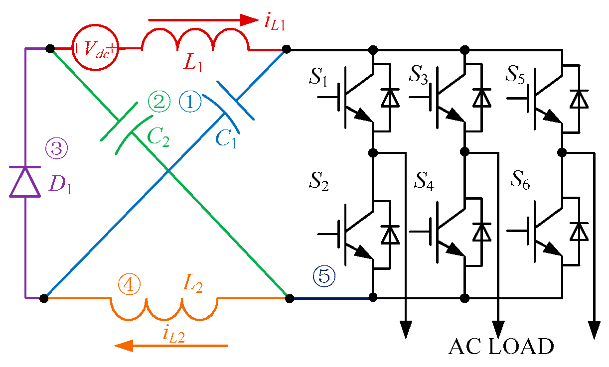
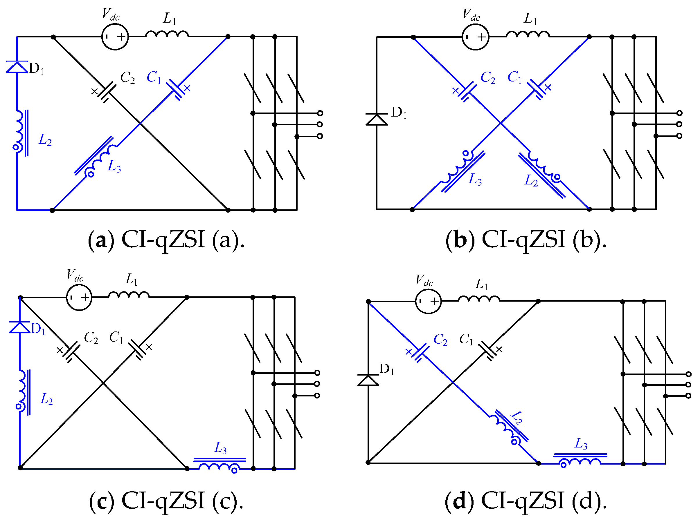
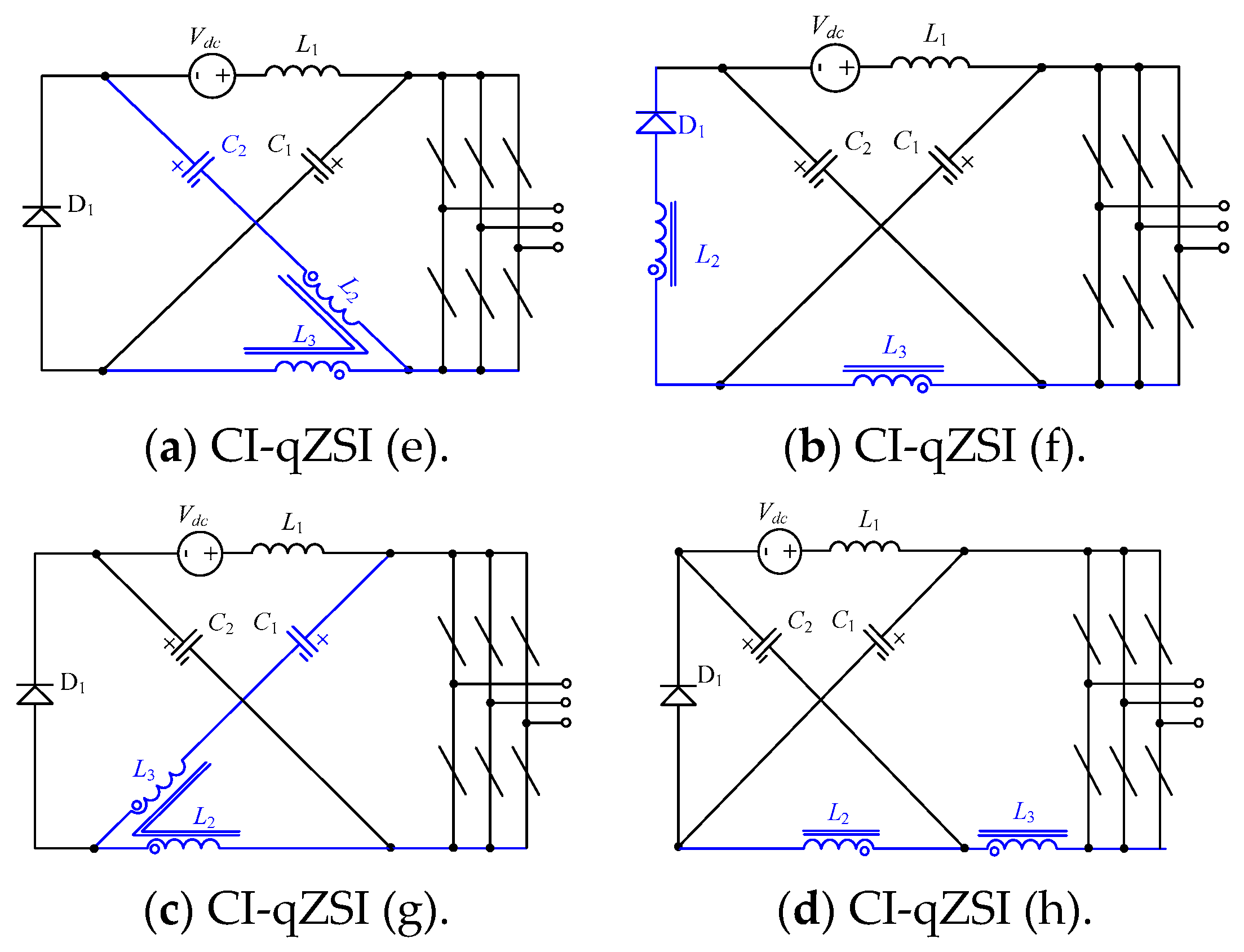
This paper deduces and discusses various topologies of coupled inductor qZSI (CL-qZSI). According to the different position arrangement of the coupled inductor, a family of CI-qZSI topology is summarized, and all feasible topologies and a detailed characteristics comparison analysis of these topologies are discussed. In the second section, the topology of CI-qZSI is derived, and the working principle of CI-qZSI is analyzed. In the third section, the characteristics of various topologies are compared and analyzed, including the voltage stress of capacitors and diodes, output current ripple, the size of the coupled inductor, and circuit efficiency. In the fourth section, two representative topologies are selected for simulation and experimental verification. The fifth section summarizes the full text.

2. Topological Derivation and Operating Principle

2.1. Derivation of CI-qZSI Topologies

The input current of traditional ZSI is discontinuous, so it has a limited scope of application in renewable energy generation systems. To extend the life span of renewable energy source such as fuel cells and photovoltaic system, the input current is expected to have a small ripple. The qZSI is shown in Figure 1 is derived from traditional ZSI, while the input voltage source is in series with the inductor to get continuous input current. In addition, compared to traditional ZSI, qZSI has lower voltage stress across one capacitor. The voltage boosting capability of qZSI is the same as ZSI. Thus, it cannot provide a higher gain in low input applications. By replacing the inductor of the LC network with the coupled inductor, high step-up is achieved easily. A class of coupled inductor based quasi-Z-source inverter (CI-qZSI) can be formed regarding the position of the coupled inductor located in the topologies. Ten types of different topologies can be formed by selecting two branches as the primary and secondary winding of the coupled inductor in branch ①–⑤. We can classify these circuits into two types as shown in Figure 2 and Figure 3, based on if there is the inductance in branch ④ or not. According to the basic principle of the circuit, there are two topologies which will have short circuit fault when they work in Figure 4. Hence, eight derived topologies of CI-qZSI are considered after excluding these two topologies.

2.2. Operating Principle of CI-qZSI

CI-qZSI is operating in shoot-through and non-shoot-through states just like the traditional ZSI. Figure 3a topology (e) is analyzed to illustrate the steady-state operating principle. Considering the shoot-through duty cycle is Dsh, the input voltage is Vdc.
When diode D1 is turned off, both of the switches in the same bridge are conducted, while the circuit operates in the shoot-through state, the equivalent circuit is shown in Figure 5a, so:
{ V d c + v C 2 + v L 2 _ s h o o t = v L 1 _ s h o o t v L 3 _ s h o o t = v C 1
When diode D1 is turned on, the DC link side can be considered as a current source, while the circuit operates in non-shoot-through state, the equivalent circuit is shown in Figure 5b, we can get:
{ V d c = V L 1 _ n o n s h o o t + v C 1 v L 3 _ n o n s h o o t + v L 2 _ n o n s h o o t + v C 2 = 0
Consider n is the turns ratio of the coupled inductor L2, L3. In a steady-state, one switching cycle of average inductor voltage is zero, so:
v L 2 v L 3 = n
From (1), (2) and (3), we get:
{ v C 1 = 1 D s h 1 ( 2 + n ) D s h V d c v C 2 = ( 1 + n ) D s h 1 ( 2 + n ) D s h V d c
The peak DC link voltage v ^ i can be derived as:
v ^ i = 1 1 ( 2 + n ) D s h V d c = B V d c
The output peak phase voltage v ^ o can be expressed as:
v ^ o = 1 2 M v ^ i = 1 2 M B V d c
B = 1 1 ( 2 + n ) D s h
where M is the modulation ratio and B is the boost factor.
The same analysis method can be applied to other CI-qZSI topologies because of the same operating principle. CI-qZSI can be classified into three types regarding the various gain expression of peak DC link voltage, as shown in Table 1.

3. Comparison of CI-qZSI Characteristics

3.1. Capacitor and Diode Voltage Stress

In the same design specifications, the eight topologies are designed under same conditions of maximum boost factor Bmax, DC link peak vi, the lowest input voltage Vdc_min, and output peak phase voltage vo_max. It is easy to find that in each topology modulation ratio M and shoot-through duty cycle 
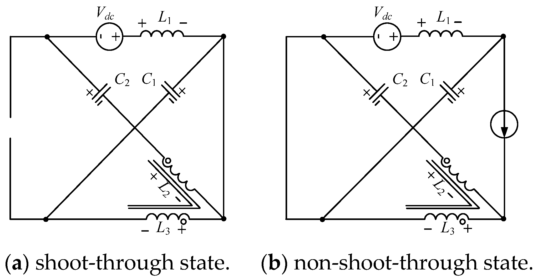
Dsh keep equal in each topology. For example, the average state of the topology is analyzed in CI-qZSI (e) in Figure 3. Based on this point, in one period the average voltage across the inductor is 0, so:
V d c _ min + v C 2 = v C 1
Through analysis under steady state, we can derive:
V d c _ min + v C 2 = v C 1 = v i  
It is easy to get:
v C 2 = v D 1 ( a v e r a g e )
Other topologies also have the same expression. Hence, with similar design parameters, switch voltage stress, diode voltage stress vD1, and capacitor voltage stresses vC1, vC2 of all other topologies, it is same. In the turn-on state, the voltage of the diode is 0. The diode withstands reverse voltage vD1 when turns off. Because the time of turn-on or turn-off is the same, the voltage stress of the diode is also equal. The corresponding information is listed in Table 2.

3.2. Effect of Shoot-Through Duty Cycle and Turns Ratio on the Boost Factor

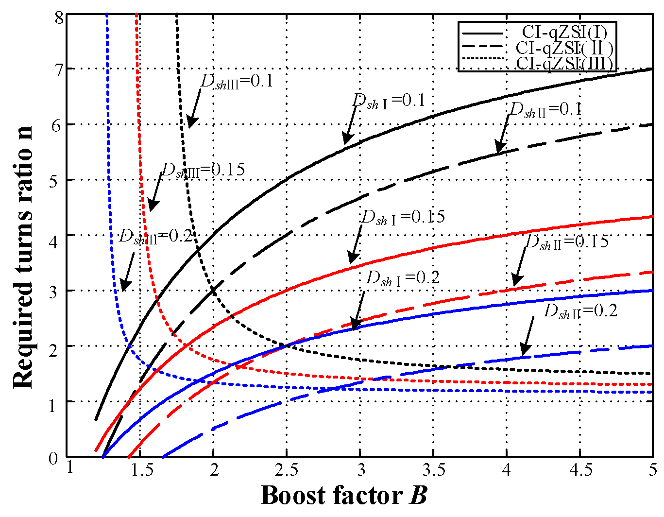
The relationships of the turn ratio and boost factor of three types of CI-qZSI are shown in Figure 6. The boosting capability of CI-qZSI (Ⅱ) is not only higher than that of CI-qZSI (Ⅰ), but also the required turns ratio under the same boot ratio and the shoot-through duty cycle is less. When the turns ratio of CI-qZSI (Ⅲ) gets close to one, it exhibits higher boost capability than CI-qZSI (Ⅱ) and CI-qZSI (Ⅰ). The boost ratio of CI-qZSI (Ⅲ) declines when its turns ratio slightly increases more than one. The boost feature of CI-qZSI varies with the shoot-through duty cycle and turns ratio of CI-qZSI. Thus, each topology has a different scope of applications.
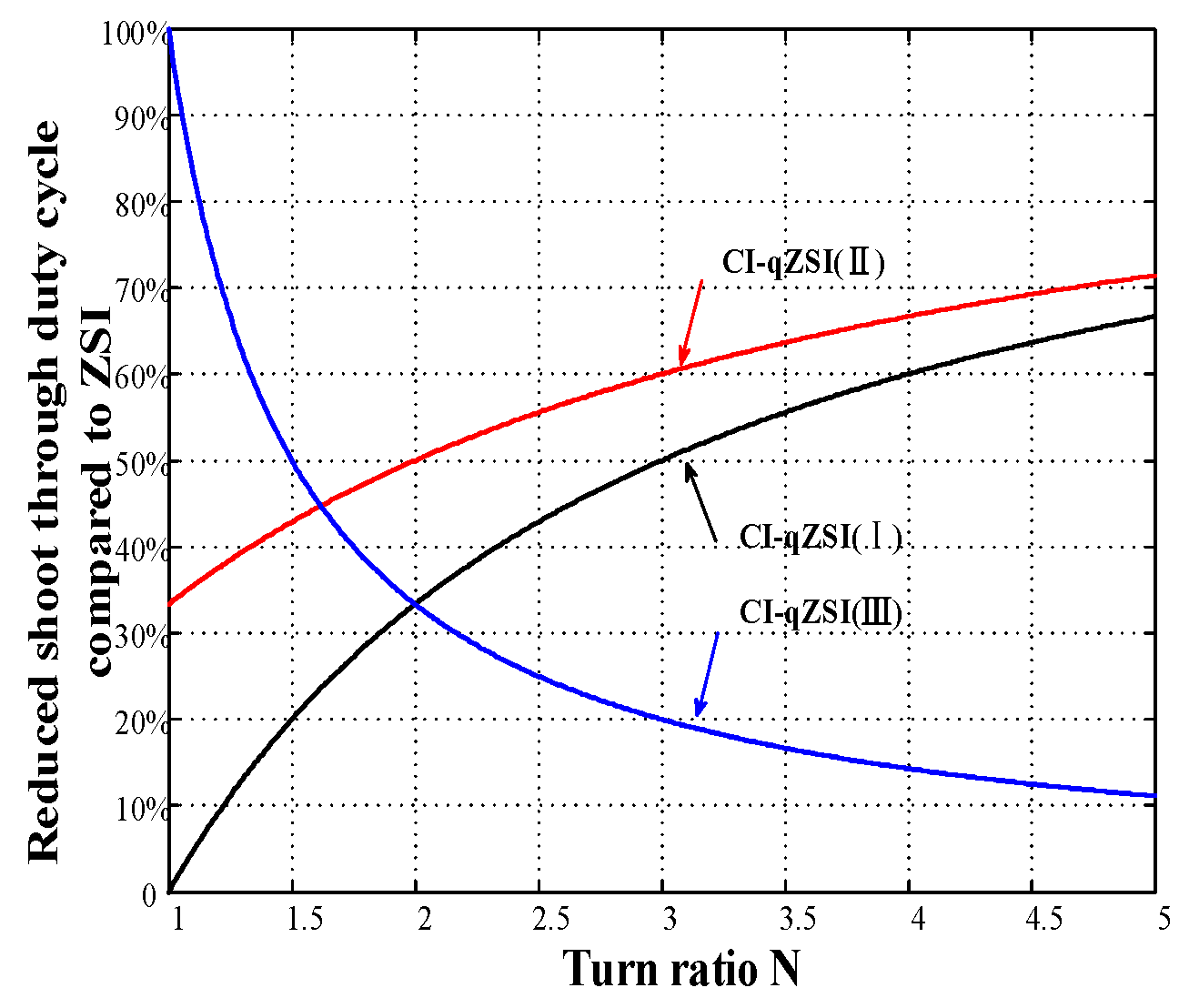
Figure 7 illustrates the reduced duty cycle of three types of CI-qZSI. CI-qZSI gets the same boost capability by using less shoot-through time compared to the traditional ZSI under the same boost factor B. When the boosting factor and turns ratio is the same, CI-qZSI (Ⅱ) needs a smaller shoot-through duty cycle as compared to the CI-qZSI (Ⅰ). When the turns ratio of CI-qZSI (Ⅲ) is closed to one, its voltage gain can get higher and its shoot-through duty cycle can be greatly reduced. When the turns ratio of CI-qZSI (Ⅲ) increases, a reduced percentage of shoot-through duty ratio lowers.

3.3. Volume Comparison of Coupled Inductor

From the above analysis, it is clear that these eight topologies have the same voltage stress of active and passive components if the design parameters remain the same. If these inverters operate under equal load, then the average input current value and ripples are also the same. Hence, a comparison of eight topologies mainly depends upon coupled inductor’s volume and turns ratio. These factors will decide the cost of the inverter. Hence, it is vital to design and compare the volume of the coupled inductor under the most severe operating conditions.
In terms of the DC/DC converter, the amount of energy stored in the core is proportional to the required volume of the core, where magnetizing inductance of the inductor is Lm, volume of the core is AeWa, the root-mean-square of magnetizing inductor’s current is Im, and the peak value of magnetizing inductors current is im_pk. The LC network for CI-qZSI can be assumed as a DC/DC converter. Therefore, the comparison of the coupled inductor in CI-qZSIs can be replaced by the comparison of the value AeWa shown in Equation (11).
A e W a 1 2 L m I m i m _ p k
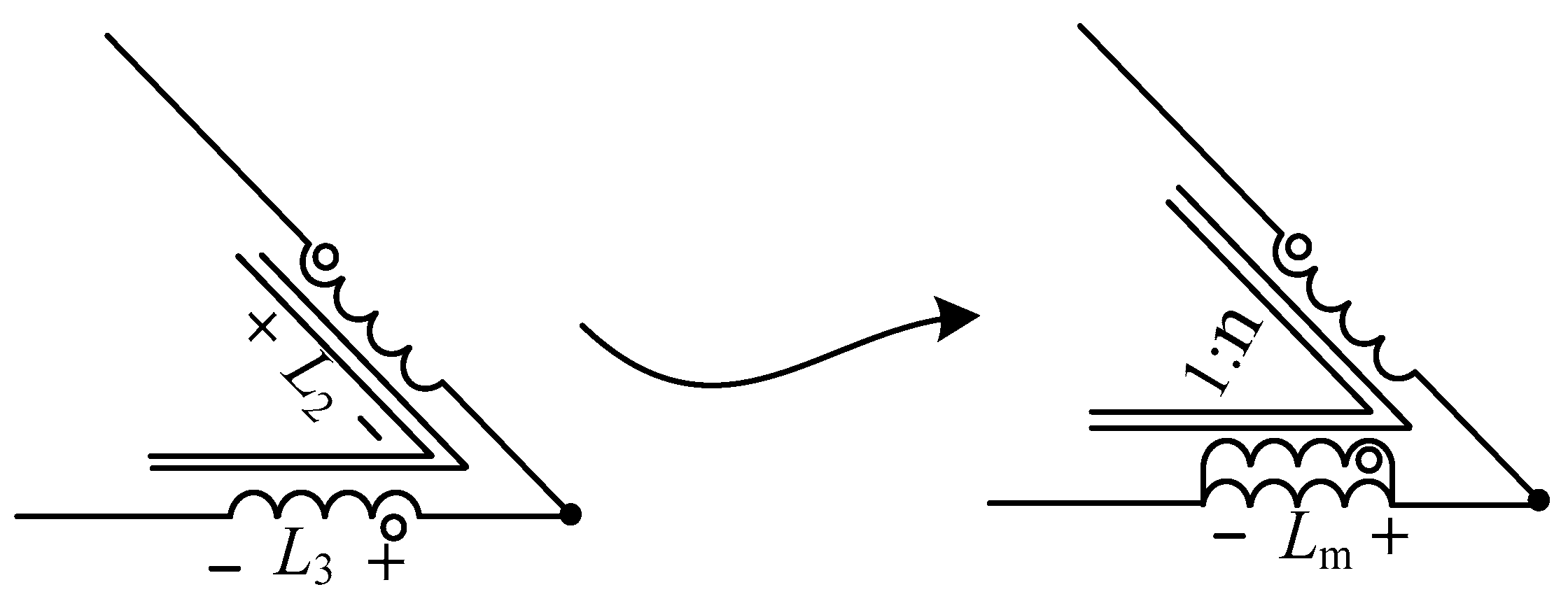
Consider CI-qZSI (e) topology as shown in Figure 3a, an ideal transformer parallel with the magnetizing inductor is equivalent to the coupled inductor L2, L3, as shown in Figure 8. The output power is Po. In the worst situation, the average current of the magnetizing inductor is:
I a v e r a g e = P o V d c _ min
When the inverter operates in the shoot-through mode, the coupled inductor’s voltage can be used to determine the value of magnetizing inductance, as Equation (13) shows below:
L m = V L Δ t Δ i = V C 1 ( 1 D s h ) T / I a v e r a g e Δ i / I a v e r a g e
Δ i I m = k %
i m _ p k = I a v e r a g e + Δ i 2
where k is the coupled inductor’s current ripple factor, the RMS (Root Mean Square) current is replaced by the average value approximately, and when the magnetizing inductor operates in continuous mode, from (11)–(15) we can get:
A e W a V L _ s h o o t I m V L _ s h o o t I a
In Equation (16), volume comparison of the coupled inductor can be reformed to a comparison of the product of Ia and VL_shoot. Other CI-ZSI topologies are analyzed by following the same method. The detailed comparisons are listed in Table 3.
CI-qZSI can be classified into four categories to the value of coupled inductor’s volume: (1) class A includes CI-qZSI (a), (f), (g); (2) class B includes CI-ZSI (c); (3) class C includes CI-ZSI (d), (e), (h); (4) class D includes CI-ZSI (b). From the above analysis, the weight and volume of class A coupled inductors are less than class B. In the other three classes of CI-ZSI, when 1 − 2 Dsh > 1/Bmax, the coupled inductor’s volume of class B is bulkiest, followed by class A, and the coupled inductor’s volume of class C is minimum. When 1 − 1/Bmax > Dsh, the volume of the coupled inductor of class C is maximum followed by class B, while class A has the smallest volume. When the value of 1/B lies between [1 − Dsh,1 − 2 Dsh], the coupled inductor’s volume of class C lies between class B and class A. The coupled inductor of class D acquires the least weight and volume, no average current is flowing through class D coupled inductor as compared to the first three CI-qZSI topologies.

3.4. Input Current Ripple

As is shown in Figure 5a, the expression of input current ripple in the shoot-through state is:
Δ i = V L L D s h T
According to KVL, we get:
Δ i = V c 1 + V L 2 L D s h T
From (3) and (7), we get:
Δ i = ( B 1 B D s h 1 ) V c 1 L D s h T
Similarly, all of the CI-qZSI can be classified into four categories with the value of input current ripple. Specific values and classifications are as follows in Table 4.
The value of filtering inductor L1 is designed according to the value of input current ripple, same as the volume of coupled inductors. The filtering inductors of these eight topologies can be divided to four kinds, but they are opposite to the volume of coupled inductors.

3.5. Efficiency Analysis

The power loss of eight types of converters is mainly composed of the loss of switches Pmos, the losses of diodes PD, the losses of filtering inductor PL1, coupled inductor PCL, and other small losses.
P l o s s = P m o s + P D + P L 1 + P C L + P o t h e r
According to the analysis in Section 3.1, the current and voltage stress of switch components are the same in all topologies. The main difference is the loss of filtering inductor PL1 and coupled inductor PCL. the coil (PCu) and core losses (PFe) have a very important relationship with the volume of the magnetic core (Vcore). However, the volume of filtering inductor and coupled inductor are inversed according to the analysis in Section 3.3 and Section 3.4. The dominated semiconductor loss of all topologies is the same, and the losses of magnetic elements have small differences according to practical working conditions but occupy only a small percentage. Therefore, the efficiency of all topologies is close to each other.

4. Simulation and Experiment Results

When the boost capacity is the same, the turns ratio of the coupling inductance required by CI-qZSI (Ⅱ) is the smallest. When the turns ratio of the coupling inductor is close to one, the boost capability of CI-qZSI (Ⅲ) is the best. Choose the representative topology of these two topologies for experiment. 
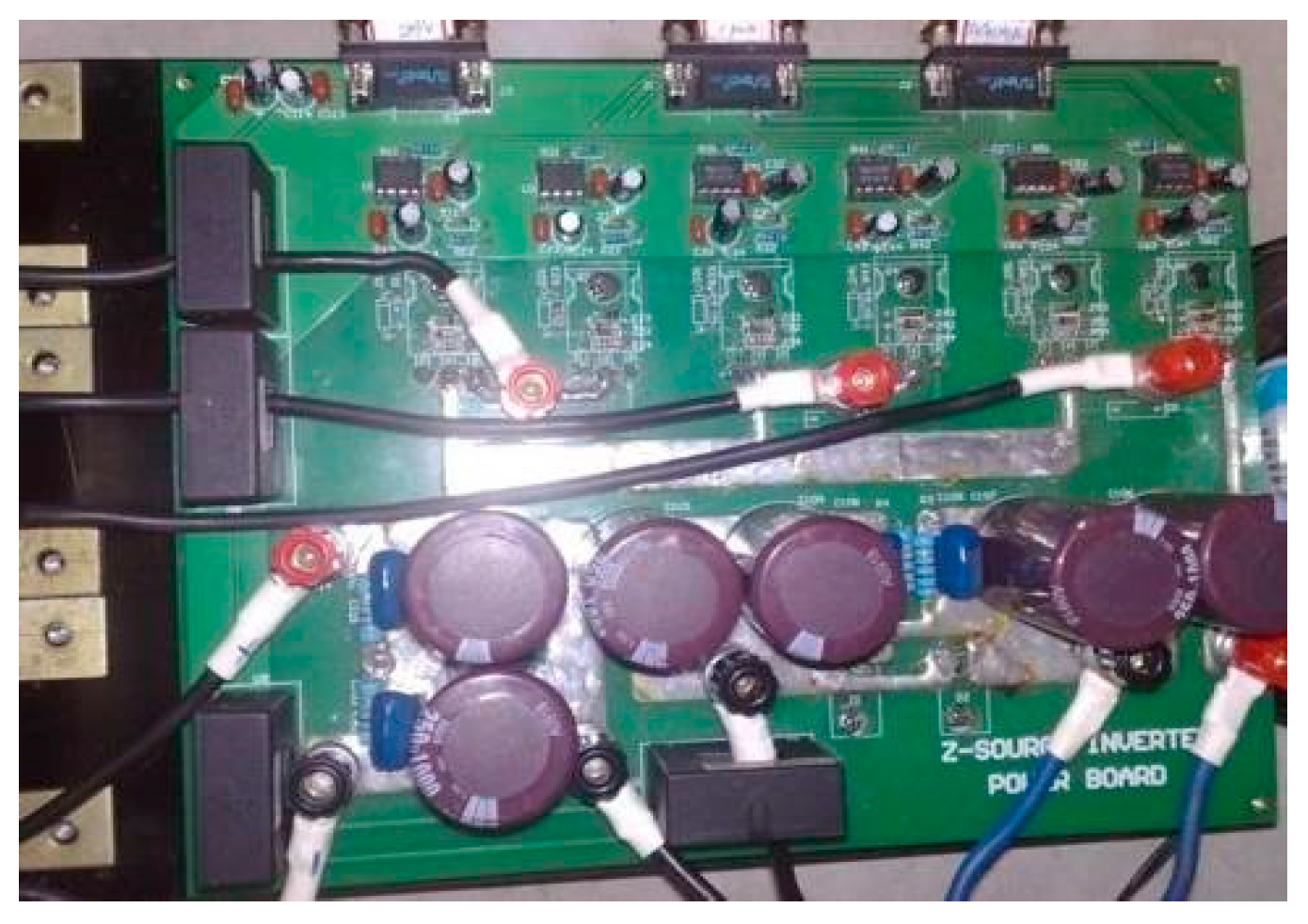
Figure 9 shows the experiment prototype, CI-qZSI’s operating modes can be classified into boost mode and buck mode, compared to the traditional Z source inverter. When the time of the shoot-through is zero, the LC network of CI-qZSI does not boost voltage, and the circuit operates in buck mode. When the time of shoot-through is not zero, the LC network of CI-qZSI boosts voltage, and the circuit operates in boost mode.
Experimental parameters are shown in Table 5. The traditional modulation strategy applied to the Z source is also suitable for the CI-qZSI. This paper adopts the SVPWM of a single-phase shoot-through method to generate the modulated signal.
Figure 10 and Figure 11 show the operating waveforms under buck mode in simulation and experiment.
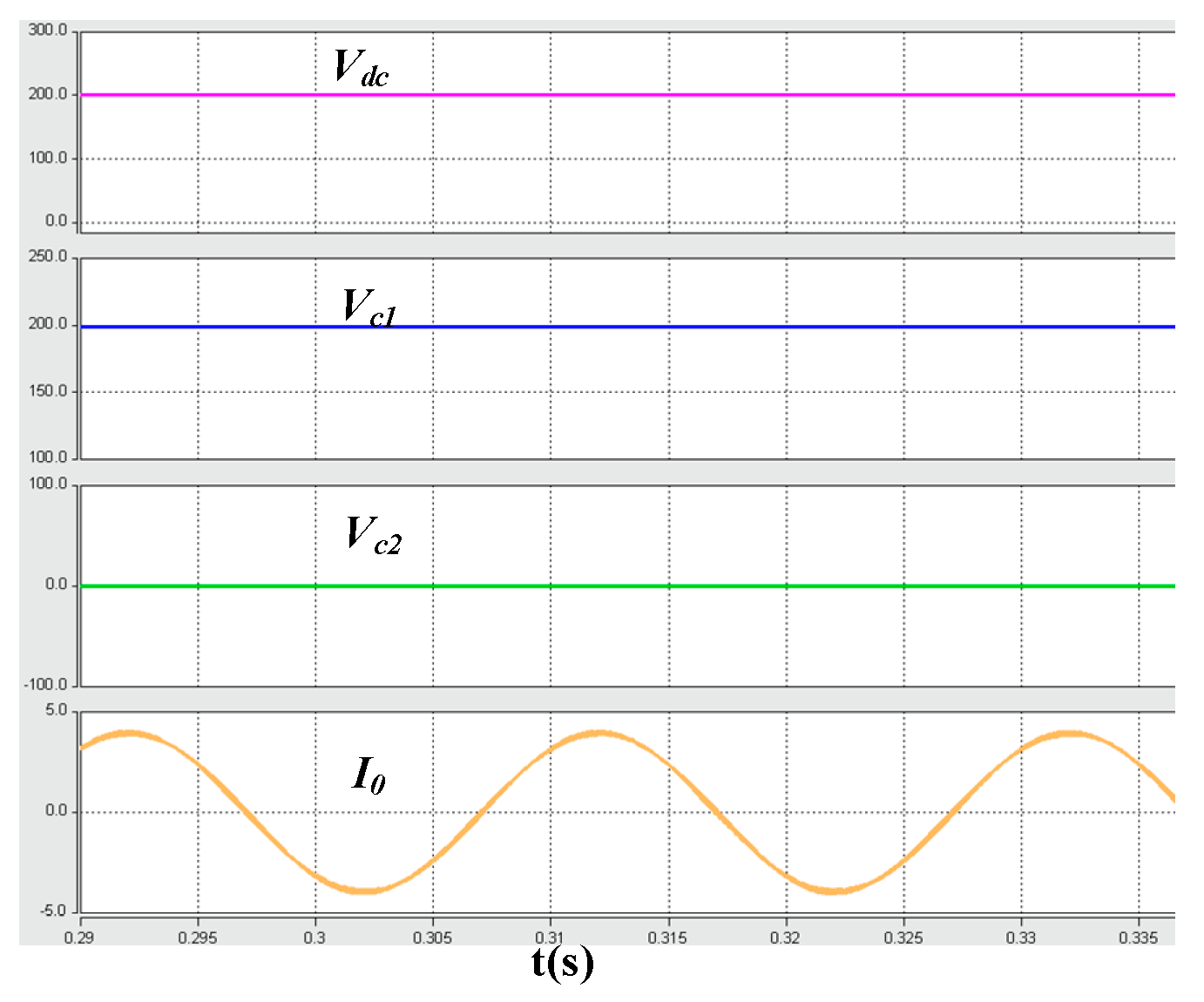
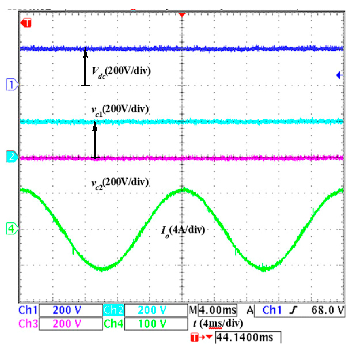
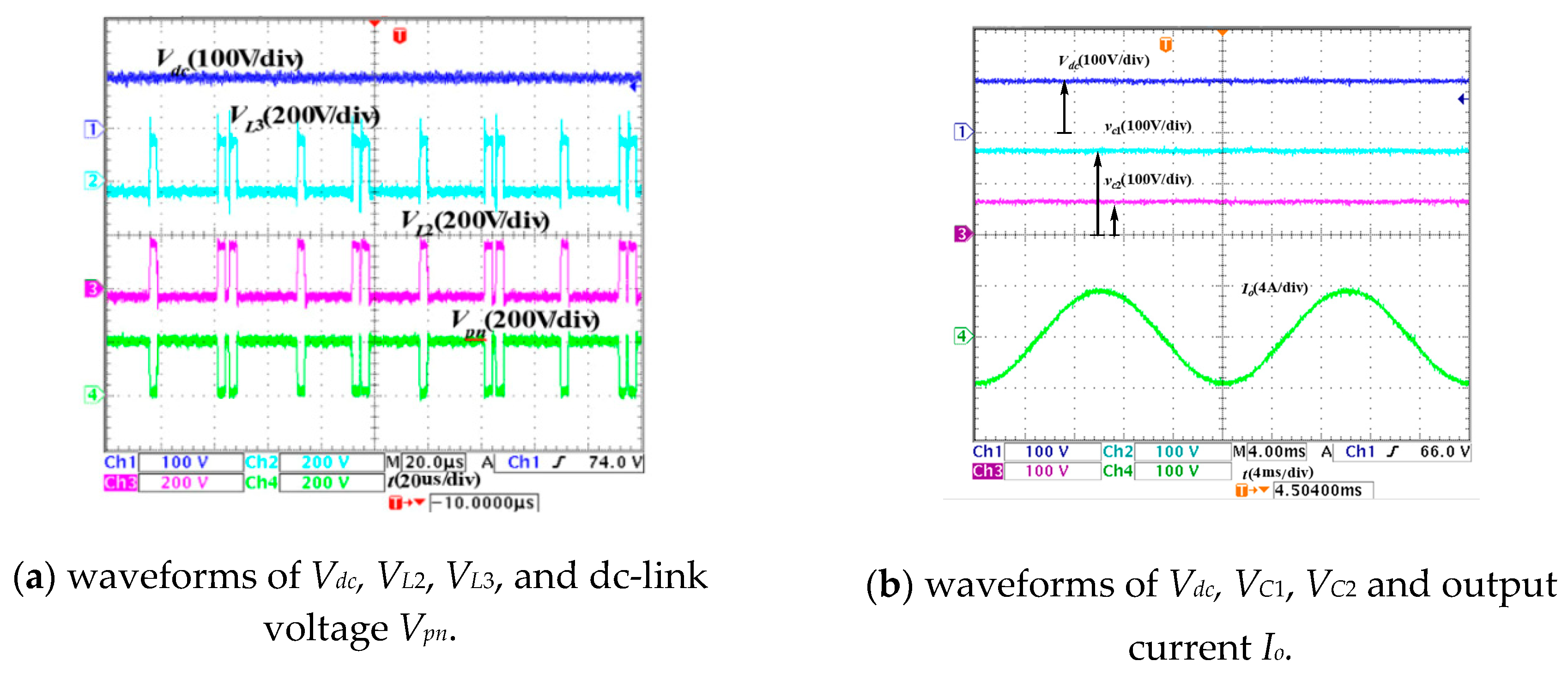
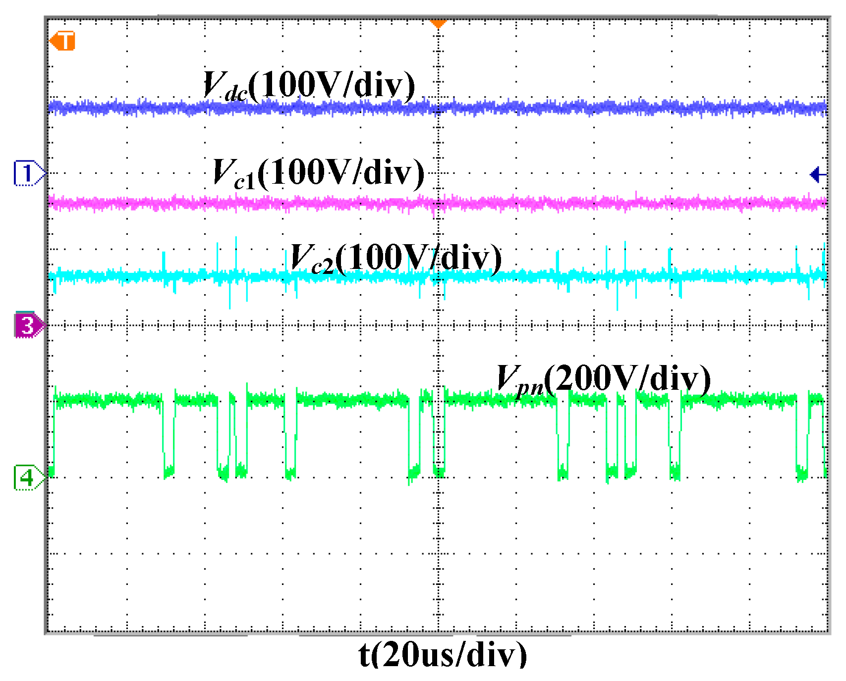
 Figure 12 and Figure 13 show the waveforms in boost mode in simulation and experiment. The DC link voltage pulsed six times in one switching period (100 µs). In shoot-through state, the value of voltage is zero. In non-shoot-through mode, the value of voltage is 200 V. When the boost ratio of CI-ZSI (e) is 2, The shoot-through duty cycle is 0.18, while ZSI needs 0.25. Hence, to get the same boost ratio, CI-qZSI shoot-through time is significantly less than ZSI. Thus, experimental and simulation results coincide with the analysis well.
In buck mode, the operation modes of different circuits are completely equivalent to that of qZSI, and the principle waveforms are the same. Therefore, only the comparison between simulation and experiment in boost mode is given in the following. 
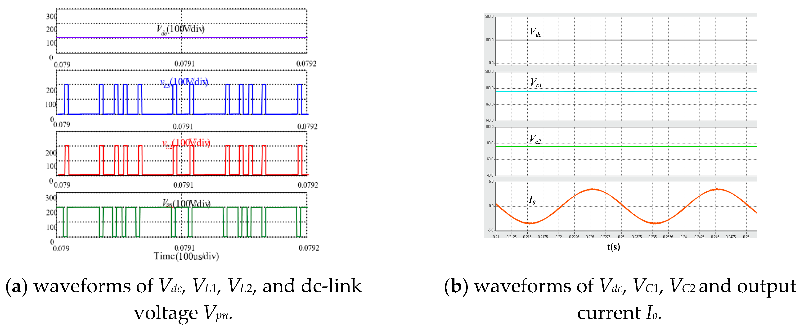
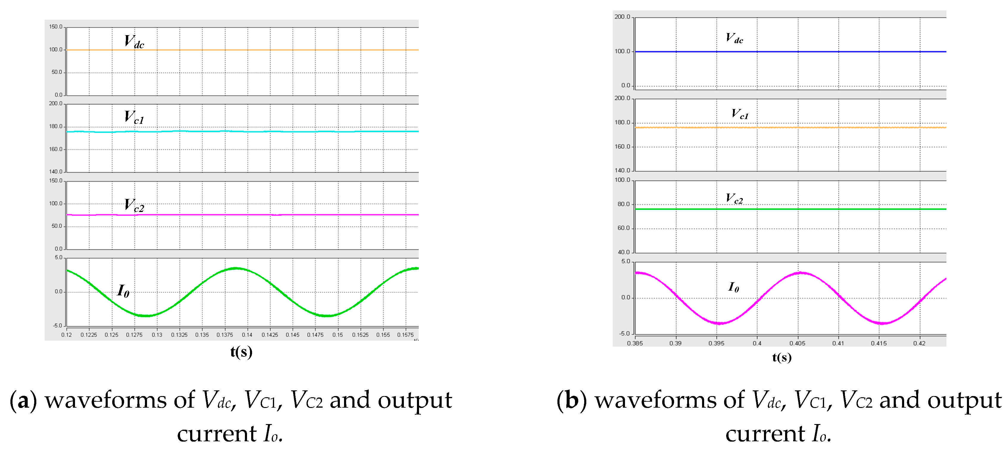
Figure 14 shows the simulation waveforms of CI-qZSI (a) and (g) in boost mode. The shoot-through duty ratio and boosting ratio are the same as CI-qZSI (e) (CI-qZSI (a) belongs to CI-qZSI (Ⅰ), CI-qZSI (e) belongs to CI-qZSI (Ⅱ), CI-qZSI (g) belongs to CI-qZSI (Ⅲ)). According to voltage gain listed in TABLE I, the turns ratio of the three circuits meets the requirements: n 1 = n 2 + 1 = n 3 n 3 1 (n1 = 2, n2 = 1, n3 = 2). It can be seen from the simulation that the capacitance-voltage and output current in the three circuits are equal. The experimental waveform of CI-qZSI (g) in boost mode is shown in Figure 15, and the capacitor voltage and DC-link voltage are consistent with the simulation results. From the verifications of different topologies, we can see that under the same shoot-through duty ratio, the capacitor voltage Vc1, Vc2 and DC-link voltage Vdc are the same.

5. Conclusions

Compared to the traditional Z-source inverter, the CI-qZSI has the following advantages: 1. Without adding passive components, a higher boost ratio can be obtained; 2. It can maintain the continuity of input current; 3. The components are subject to less voltage stress. From the regularity of the qZSI, this paper supplements the qZSI with coupled inductors that have been proposed in the existing literature, and it derives a family of qZSI with coupled inductors. By summarizing and categorizing all topologies, we determine: 1. Under the same turns ratio, CI-qZSI (e) CI-qZSI (f) has a stronger boosting ability; 2. under the same boost capacity, CI-qZSI (d) interchangeable inductors have a smaller volume; and 3. under the same operating parameters, CI-qZSI (c) has the smallest current ripple. Through analyzing all aspects of each variable, a suitable application place can be found.

Author Contributions

Conceptualization, Y.T., H.S. and S.W.; methodology, Y.T., H.S. and S.W.; software, H.S.; validation, Y.T., H.S. and S.W.; investigation, H.S. and S.W.; writing—original draft preparation, H.S.; writing—review and editing, Y.T., H.S. and S.W.; supervision, Y.T., H.S. and S.W. All authors have read and agreed to the published version of the manuscript.

Funding

The publication has been financed using a subsidy for maintenance and development of research potential and received no external funding.

Conflicts of Interest

The authors declare no conflict of interest.

References

  1. Yuan, J.; Yang, Y.; Blaabjerg, F. A Switched Quasi-Z-Source Inverter with Continuous Input Currents. Energies 2019, 13, 1390. [Google Scholar] [CrossRef] [Green Version]
  2. Stepenko, S.; Husev, O.; Vinnikov, D.; Roncero-Clemente, C.; Pimentel, S.P.; Santasheva, E. Experimental Comparison of Two-Level Full-SiC and Three-Level Si–SiC Quasi-Z-Source Inverters for PV Applications. Energies 2019, 12, 2509. [Google Scholar] [CrossRef] [Green Version]
  3. Mohammadi, M.; Moghani, J.S.; Milimonfared, J. A Novel Dual Switching Frequency Modulation for Z-Source and Quasi-Z-Source Inverters. IEEE Trans. Ind. Electron. 2018, 65, 5167–5176. [Google Scholar] [CrossRef]
  4. Minh-Khai, N.; Youn-Ok, C. Maximum Boost Control Method for Single-Phase Quasi-Switched-Boost and Quasi-Z-Source Inverters. Energies 2017, 10, 553. [Google Scholar]
  5. Liu, J.; Wu, J.; Qiu, J.; Zeng, J. Switched Z-Source/Quasi-Z-Source DC-DC Converters with Reduced Passive Components for Photovoltaic Systems. IEEE Access 2019, 7, 40893–40903. [Google Scholar] [CrossRef]
  6. Li, Z.; Pu, S.; Chen, Y.; Wei, R. An Integration Optimization Strategy of Line Voltage Cascaded Quasi-Z-Source Inverter Parameters Based on GRA-FA. Energies 2020, 13, 4391. [Google Scholar] [CrossRef]
  7. Ghosh, S.; Sarkar, K.; Maiti, D.; Biswas, S.K. A single-phase isolated Z-source inverter. In Proceedings of the 2016 2nd International Conference on Control, Instrumentation, Energy & Communication (CIEC), Kolkata, India, 18 July 2016; pp. 339–342. [Google Scholar]
  8. Yuan, J.; Guo, Q.; Liu, P.; Shen, Y.; Qiu, Z.; Blaabjerg, F. An Embedded Enhanced-Boost Z-Source Inverter. In Proceedings of the 2018 IEEE International Power Electronics and Application Conference and Exposition (PEAC), Shenzhen, China, 4–7 November 2018; pp. 1–6. [Google Scholar]
  9. Sharifi, S.; Monfared, M. Modified Series and Tapped Switched-Coupled-Inductors Quasi-Z-Source Networks. IEEE Trans. Ind. Electron. 2019, 66, 5970–5978. [Google Scholar] [CrossRef]
  10. Haji-Esmaeili, M.M.; Babaei, E.; Sabahi, M. High Step-Up Quasi-Z Source DC-DC Converter. IEEE Trans. Power Electron. 2020, 67, 4547–4555. [Google Scholar]
  11. Li, D.; Loh, P.C.; Zhu, M.; Gao, F.; Blaabjerg, F. Cascaded Multicell Trans-Z-Source Inverters. IEEE Trans. Power Electron. 2013, 28, 826–836. [Google Scholar]
  12. Vinnikov, D.; Roasto, I.; Strzelecki, R.; Adamowicz, M. Step-Up DC-DC Converters with Cascaded Quasi-Z-Source Network. IEEE Trans. Ind. Electron. 2011, 59, 3727–3736. [Google Scholar] [CrossRef]
  13. Li, L.; Tang, Y.; He, Y. Coupledinductor based high set-up quasi Z-source inverters. In Proceedings of the 2014 IEEE 9th Conference on Industrial Electronics and Applications (ICIEA), Hangzhou, China, 9–11 June 2014. [Google Scholar]
  14. Dong, S.; Zhang, Q.; Zhou, C.; Cheng, S. Analysis and design of snubber circuit for Z-source inverter. In Proceedings of the 2014 16th European Conference on Power Electronics and Applications, Lappeenranta, Finland, 26–28 August 2014; pp. 1–10. [Google Scholar]
  15. Forouzesh, M.; Abdelhakim, A.; Siwakoti, Y.; Blaabjerg, F. Analysis and design of an energy regenerative snubber for magnetically coupled impedance source converters. In Proceedings of the 2018 IEEE Applied Power Electronics Conference and Exposition (APEC), San Antonio, TX, USA, 4–8 March 2018; pp. 2555–2561. [Google Scholar]
  16. Strzelecki, R.; Adamowicz, M.; Strzelecka, N. New type T-source inverter. In Proceedings of the Compatibility and Power Electronics, Badajoz, Spain, 20–22 May 2009; pp. 191–195. [Google Scholar]
  17. Liu, H.; Zhou, B.; Li, Y. High-Efficiency T-Source Inverter with Low Voltage Spikes Across the Switch Bridge. IEEE Trans. Power Electron. 2020, 35, 10554–10566. [Google Scholar] [CrossRef]
  18. Reddivari, R.; Jena, D. A Negative Embedded Differential Mode Γ-Source Inverter with Reduced Switching Spikes. IEEE Trans. Circuits Syst. 2020, 7, 2009–2013. [Google Scholar] [CrossRef]
  19. Deepankar; Chauhan, A.K.; Singh, S.K. Integrated Dual-Output L-Z Source Inverter for Hybrid Electric Vehicle. IEEE Trans. Transp. Electr. 2018, 4, 732–743. [Google Scholar] [CrossRef]
  20. Surapaneni, R.K.; Das, P. A Z-Source-Derived Coupled-Inductor-Based High Voltage Gain Microinverter. IEEE Trans. Ind. Electron. 2017, 65, 5114–5124. [Google Scholar] [CrossRef]
  21. Battiston, A.; Miliani, E.H.; Pierfederici, S. A Novel Quasi-Z-Source Inverter Topology with Special Coupled Inductors for Input Current Ripples Cancellation. IEEE Trans. Power Electron. 2015, 31, 2409–2416. [Google Scholar] [CrossRef] [Green Version]
  22. Banaei, M.R.; Oskouei, A.B.; Dehghanzadeh, A. Extended switching algorithms based space vector control for five-level quasi-Z-source inverter with coupled inductors. IET Power Electron. 2014, 7, 1509–1518. [Google Scholar] [CrossRef]
  23. Peng, W.; Liu, P.; He, M. Electro-thermal Analysis of the Coupled Inductor for Quasi-Z Source Inverters. In Proceedings of the 2019 22nd International Conference on Electrical Machines and Systems (ICEMS), Harbin, China, 11–14 August 2019. [Google Scholar]
  24. Zhao, Z.; Muhammad, M.; Armstrong, M. Quasi-Z-source Inverter with Coupled Inductor. In Proceedings of the 2019 IEEE Conference on Power Electronics and Renewable Energy (CPERE), Aswan City, Egypt, 23–25 October 2019. [Google Scholar]
  25. Samadian, A.; Hosseini, S.H.; Sabahi, M. A New Coupled Inductor Non-isolated High step up Quasi Z-Source DC-DC Converter. IEEE Trans. Ind. Electron. 2019, 67, 5389–5397. [Google Scholar] [CrossRef]
Figure 1. Quasi-Z-source inverter.
Energies 13 05667 g001
Figure 2. CI-qZSI topologies without inductance in ④.
Energies 13 05667 g002
Figure 3. CI-qZSI topologies with inductance in ④.
Energies 13 05667 g003
Figure 4. Wrong CI-qZSI topologies.
Energies 13 05667 g004
Figure 5. Equivalent circuit of CI-qZSI (e).
Energies 13 05667 g005
Figure 6. Relationship of n and B.
Energies 13 05667 g006
Figure 7. Reduced shoot-through time comparison.
Energies 13 05667 g007
Figure 8. Equivalent circuit of coupled inductor.
Energies 13 05667 g008
Figure 9. The prototype of the proposed converter.
Energies 13 05667 g009
Figure 10. Simulation waveforms in buck mode.
Energies 13 05667 g010
Figure 11. Experimental waveforms in buck mode.
Energies 13 05667 g011
Figure 12. Simulation waveforms of CI-qZSI (e) in boost mode.
Energies 13 05667 g012
Figure 13. Experimental waveforms of CI-qZSI (e) in boost mode.
Energies 13 05667 g013
Figure 14. Simulation waveforms in boost mode, (a) CI-qZSI (a), (b) CI-qZSI (g).
Energies 13 05667 g014
Figure 15. Experimental waveforms of CI-qZSI (g) in boost mode.
Energies 13 05667 g015
Table 1. Classification of CI-qZSI topologies.
TypeBoost Factor BTopologies
CI-qZSI (Ⅰ) 1 1 ( 1 + n 1 ) D s h CI-qZSI (a)
CI-qZSI (b)
CI-qZSI (c)
CI-qZSI (d)
CI-qZSI (Ⅱ) 1 1 ( 2 + n 2 ) D s h CI-qZSI (e)
CI-qZSI (f)
CI-qZSI (Ⅲ) 1 1 ( 2 + 1 n 3 1 ) D s h CI-qZSI (g)
CI-qZSI (h)
Table 2. Voltage stress of CI-qZSI topologies.
CategoryDC Bus Voltage ViCapacitor Voltage vC1Capacitor Voltage vC2Diode Voltage vD1
CI-qZSI (Ⅰ) S D ¯ B max V d c _ min ( B max B max D s h ) V d c _ min ( B max 1 B max D s h ) V d c _ min S D ( B max 1 B max D s h ) V d c _ min D s h
CI-qZSI (Ⅱ) S D ¯ B max V d c _ min ( B max B max D s h ) V d c _ min ( B max 1 B max D s h ) V d c _ min S D ( B max 1 B max D s h ) V d c _ min D s h
CI-qZSI (Ⅲ) S D ¯ B max V d c _ min ( B max B max D s h ) V d c _ min ( B max 1 B max D s h ) V d c _ min S D ( B max 1 B max D s h ) V d c _ min D s h
where, S D represent the shoot-through state of bridge arms, when a bridge arm is in the shoot-through state, S D is 1 and S D ¯ is 0.
Table 3. Volume comparison of coupled inductors in CI-qZSI topologies.
TopologiesVL_shootIaverageVL_shootImClassification
CI-qZSI (a) ( B max B max D s h ) V d c _ min n a P o V d c _ min B max 1 B max D s h B max D s h ( 1 D s h ) B max P o A
CI-qZSI (b) ( B max B max D s h ) V d c _ min 00D
CI-qZSI (c) ( B max B max D s h ) V d c _ min ( n c + 1 ) P o V d c _ min B max 1 B max D s h ( 1 D s h ) B max P o B
CI-qZSI (d) ( B max B max D s h ) V d c _ min P o V d c _ min ( 1 D s h ) B max P o C
CI-qZSI (e) ( B max B max D s h ) V d c _ min P o V d c _ min ( 1 D s h ) B max P o C
CI-qZSI (f) ( B max B max D s h ) V d c _ min ( n f + 1 ) P o V d c _ min B max 1 B max D s h B max D s h ( 1 D s h ) B max P o A
CI-qZSI (g) ( B max B max D s h ) V d c _ min n g 1 n g P o V d c _ min B max 1 B max D s h B max D s h ( 1 D s h ) B max P o A
CI-qZSI (h) ( B max B max D s h ) V d c _ min n h 1 ( n h 1 ) P o V d c _ min ( 1 D s h ) B max P o C
Table 4. Input current ripple of CI-qZSI topologies.
TopologiesInput Current Ripple Δi
CI-qZSI (a)
CI-qZSI (f)
CI-qZSI (g)
V c 1 L D s h T
CI-qZSI (b) ( B 1 B D s h ) V c 1 L D s h T
CI-qZSI (c) 0
CI-qZSI (d)
CI-qZSI (e)
CI-qZSI (h)
( B 1 B D s h 1 ) V c 1 L D s h T
Table 5. Simulation and experimental parameters.
ParametersValueParametersValue
Input voltage Uin/V 200 ( Buck ) 100 ( Boost ) DC link voltage Vi/V 200 ( Buck ) 200 ( Boost )
L1/mH1C1,C2/µF2000
L2,L3µH 300
Turn ratio1Switching frequency fs/kHz10
Shoot-through duty cycle 0 ( Buck ) 0.18 ( Boost )
Load ( L / m H R / Ω ) 10 25 Modulation ratio 1 ( Buck ) 0.82 ( Boost )
Publisher’s Note: MDPI stays neutral with regard to jurisdictional claims in published maps and institutional affiliations.

