1. Introduction
Nowadays, the research of renewable energy is increasing due to energy shortages and pressure to reduce greenhouse gas emissions [
1]. Power converters play an important role in renewable energy conversion [
2]. Fuel cell hybrid electric vehicles need a DC–DC boost converter to suppress the variations of the fuel cell output voltage [
3,
4]. The nonlinearity of the boost converter is an obstacle when we analyze its characters [
5,
6,
7]. To overcome this problem, a linear model of the boost converter should be built. The state-space averaging method is a commonly used linear modeling method, that is, its linear small-signal model is established around the steady-state operating point [
8]. However, in the start-up process, the initial value of output voltage and the initial value of input current are both equal to zero and there is a large deviation from the target equilibrium point. The inrush current and voltage overshoot occur during the start-up process. Moreover, there is a nonminimum phase phenomenon in the control method of a boost converter based on the small-signal model, Therefore, it is impossible to deal with the system parameter changes and large-signal transient caused by start-up or load changes [
9,
10,
11].
In a practical application, the sliding mode control (SMC) has the advantages of a fast dynamic response, good stability and strong anti-disturbance ability [
12,
13,
14]. A grid voltage observer based on a sliding mode is proposed in [
15] and verified by experiments. The basic positive and negative sequences can be accurately estimated and separated for voltage sensorless operation in an unbalanced network. An extended Luenberger-sliding mode observer is proposed in [
16], which can estimate the rotor flux and resistance along with the adaptation method to compensate for the error caused by the mismatch between the motor parameter and the model in the controller. A novel adaptive-gain sliding mode observer is proposed in [
17], which can improve the precision of sensorless control of permanent magnet linear synchronous motors. In [
18], an improved sliding controller design method for the photovoltaic system is proposed, which can alleviate the disturbance caused by irradiance change and oscillation in large capacity voltage. Moreover, the controller designed by the improved method can drive photovoltaic voltage to accurately track MPPT reference value obtained from external calculation. For the quadratic boost converter, a sliding-mode controller based on a fixed-frequency pulse-width modulation (PWM) is proposed in [
19]. A feed-forward control technique is proposed in [
20] to improve the steady-state performance of the DC–DC asymmetric Multistage Stacked Boost Architecture converter. A sliding mode controller of the boost converter based on a robust pulse-width modulation is proposed in [
21], which supplies power to constant power load in typical DC micro-grid. The methods of [
19,
20,
21] do not consider the start-up situation and are only suitable for the steady-state.
The inrush current or voltage overshoot occurs in many power electronic converters during the start-up process. An input-adaptive boost converter that can start up by itself is proposed in [
22], which has the advantages of strict input regulation and high efficiency. However, due to many passive devices in a boost converter, the efficiency is reduced. The inrush current analysis is given in [
23,
24], where the auxiliary diode and inductor of a boost converter are connected in parallel to obtain the minimum inrush current. However, although the inrush current can be reduced by an auxiliary diode branch, high
du/
dt happens in the filter capacitor, which may damage the components and devices.
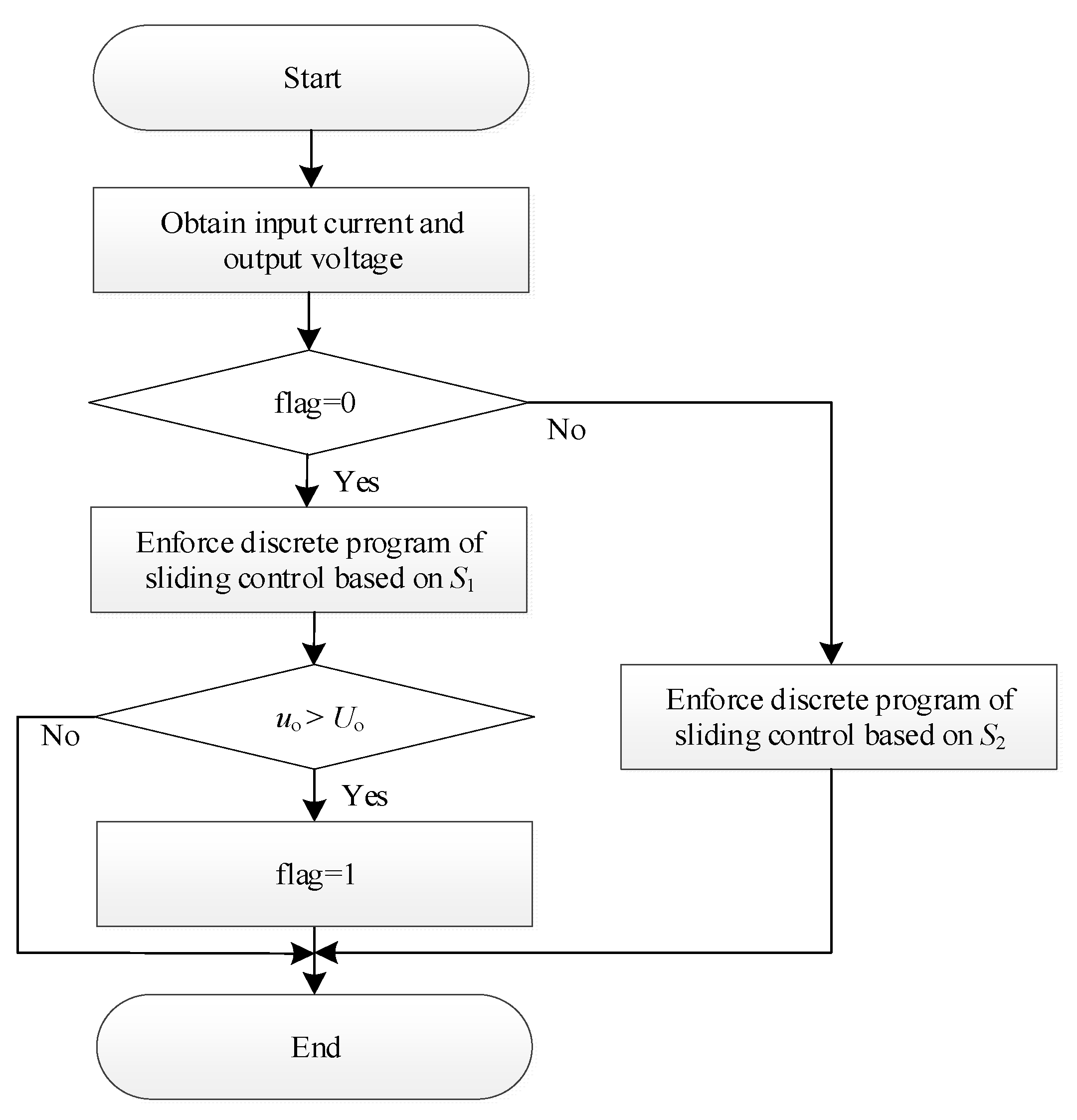
Based on the analysis given above, a sliding mode control method combining two switching surfaces is proposed for different operating conditions of the boost converter in the start-up and the steady-state in this paper. The first switching surface is based on the big-signal model for start-up processes, to reduce the inrush current and voltage overshoot. The second surface with the PI controller is adopted to regulate the output voltage and suppress the perturbation of the input voltage and load when the boost converter is in the steady-state.
The rest of this paper is arranged as follows. In
Section 2, the first switching surface
S1 (
t) is proposed in the start-up process of the boost converter, and its stability is analyzed. In
Section 3, the other switching surface
S2 (
t) is proposed to regulate the output voltage in the steady-state. After that, the proposed discrete sliding mode control strategy is implemented based on DSP in
Section 4. Then the experimental results are shown and analyzed in
Section 5. Finally, conclusions are summarized in
Section 6.
2. Sliding Control Strategy for Start-Up
Figure 1a,b corresponds to the circuit states of the boost converter in the switching-on state and switching-off state of a switching tube VT, respectively. The corresponding Equations (1) and (2) of
Figure 1a is as follows:
where
L,
iL,
uin,
C,
uo and
R represent inductor, inductor current, input voltage, capacitor, output voltage and load resistance, respectively. The corresponding Equations (3) and (4) of
Figure 1b is as follows:
Variable
p is defined as a switching state variable, if VT is switching-on,
p = 1; else
p = 0, the equations of boost converter can be expressed as:
2.1. Sliding Function for Start-Up
The average input power of the battery in one switching period is equal to the output power of load when the boost converter operates at a steady state. Ignoring the internal resistance and voltage drop of tube and diode, the relationship between
iL and
uo at steady-state is satisfied as follows:
Due to
uo >
uin, the trajectory of Equation (7) is a part of a parabola. Define
S1 (
t) as the switching surface for the start-up process, as shown below:
(
IL,
Uo) is the target equilibrium point satisfying Equation (7) at steady-state.
IL and
Uo represent the inductor current and output voltage at the target equilibrium point respectively. The sliding mode control law is shown as:
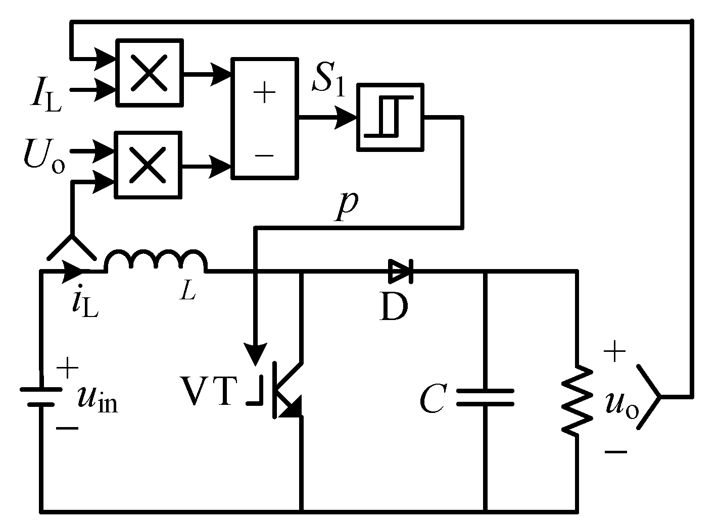
Figure 2 shows the sliding mode control model for start-up process,
iL and
uo are detected in the sampling period and substitute into Equation (8), so
S1 can be obtained. Finally, the switching signal of VT is generated by Equation (9).
2.2. Stability Analysis of the Sliding Function
Define the Lyapunov function as follows:
where the derivative of
P is:
According to Equations (5), (6) and (8), the expression of
can be obtained:
According to Equation (9), if
S1 > 0,
can be rewritten as:
Due to uo > uin > 0, so < 0.
According to the characteristics of voltage boost and current buck, iL > uo/R, so > 0.
Based on the above analysis, regardless of the value of S1, can be satisfied. Therefore, the proposed sliding mode control system is stable in this paper, iL and uo can move to the trajectory of S1 from any initial state, then reach the equilibrium point (IL, Uo) along the switching surface.
2.3. Simulation of the Sliding Mode Control Based on S1 in the Start-Up Process
The parameters of the boost converter adopted in this paper are shown in
Table 1, where the values of inductance and capacitance are satisfied as follows:
where
Dmax is the max duty,
fs is switching frequency, Δ
iLmax is the max current ripple, and
ηmax is the max voltage ripple ratio. After setting
Dmax = 0.8, Δ
iLmax = 0.5 A,
ηmax = 1%,
fs = 10 kHz, Equations (15) and (16), can get the range of
L and
C is
L > 1.9 mH and,
C > 192 μF, respectively. In this paper,
L take the value of 2 mH and
C is set to 265 μF.
The target equilibrium point is set as
IL = 1.02 A,
Uo = 24 V.
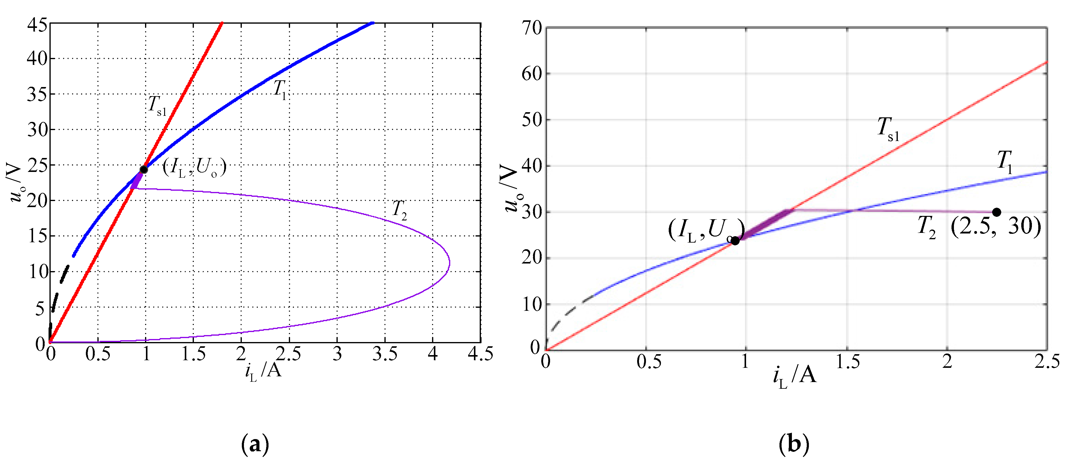
Figure 3a shows the trajectory from original point (0 A, 0 V) to the target equilibrium point (
IL,
Uo) by Matlab. The motion process of
iL and
uo is divided into two steps: Firstly, they deviate from
TS1 and increase simultaneously until
uo >
uin; then they start to approach
TS1. After that, when they reach
TS1, they move along
TS1 to the target equilibrium point (
IL,
Uo). Even if the initial point is not at the original point,
iL and
uo can still adjust to the target equilibrium point by
S1. The trajectory from the initial point (2.5 A, 30 V) to the target equilibrium point is shown in
Figure 3b.
Figure 4a shows the simulation results of the control strategy based on the small-signal model in the start-up process. For comparison,
Figure 4b shows the simulation results of the sliding mode control strategy proposed in this paper. In
Figure 4a, the peak of
iL and
uo is corresponding to 5.86 A and 28.75 V, respectively. However, there is no voltage overshoot in
Figure 4b, and the peak of
iL is only 4.12 A, which is lower than
iL shown in
Figure 4a. Moreover, current discontinuation occurs in
Figure 4a, therefore the time from the zero initial state to a steady state is much longer than
Figure 4b. The results show that the sliding mode control of
S1 is correct and feasible.
3. Voltage Control Strategy for Steady-State
Since the control strategy based on
S1 has a long time along the sliding line and poor robustness, it is only suitable for the start-up process. During steady-state, an error will occur when
uin or
R changes, therefore, another control strategy should be adopted to regulate the output voltage at this stage. Define switching surface
S2 (
t) as follows:
where Δ
iL is current error compensation. When
uin or
R is perturbed, if
Uo is constant, the target equilibrium point changes from (
IL,
Uo) to (
IL+ Δ
iL,
Uo). Δ
iL can be expressed as
where
kp is the proportional gain and
ki is the integral gain of the voltage PI controller.
t1 is the moment that the switching surface is switched from
S1 to
S2. Substituting Equation (18) into Equation (17),
S2 (
t) can be expressed as:
The sliding control law of
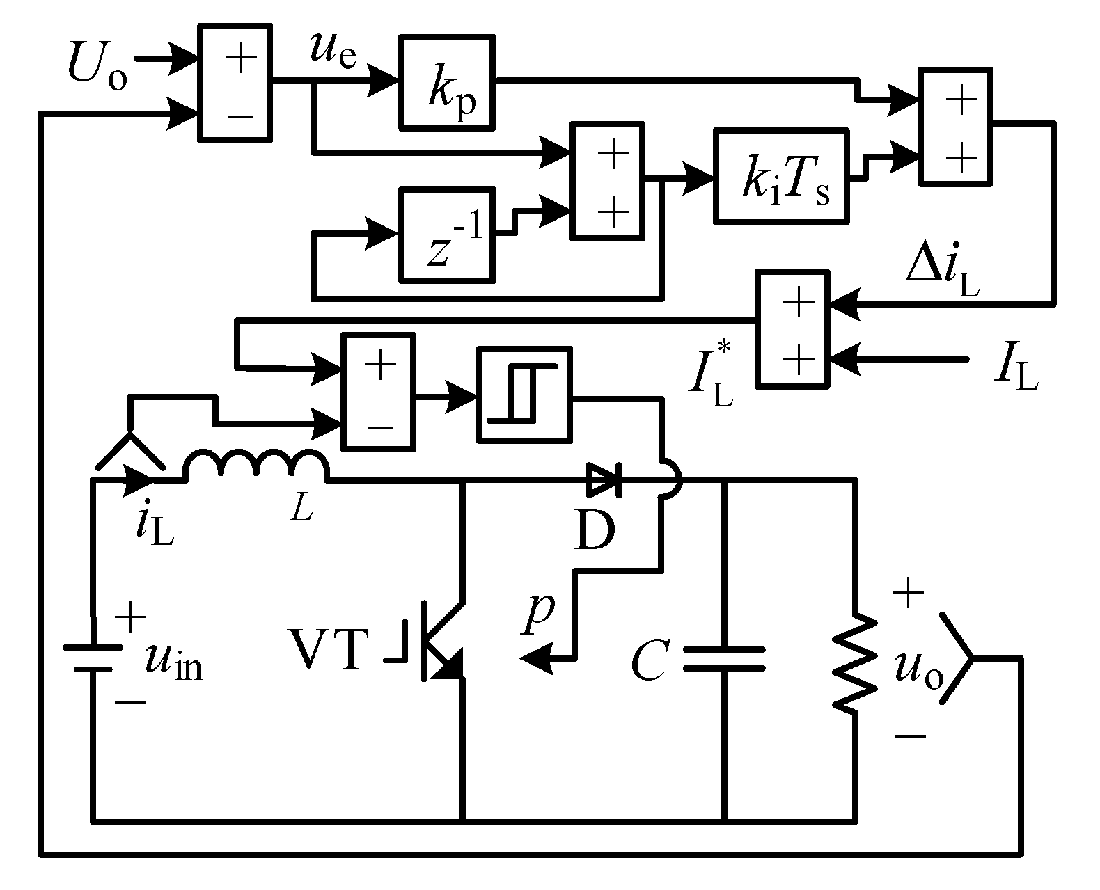
S2 is shown as:
Figure 5 shows the discrete sliding mode control model for steady-state. Δ
iL is obtained by discrete PI operation of voltage error
ue, then the switching signal of VT is generated by Equation (20).
z−1 is the delay unit, which is used to implement the discrete integral operation.
3.1. Analysis of Transient Process under Input Voltage Perturbations
Figure 6 shows the transient trajectory of
iL and
uo under different input voltage perturbations. The increase or decrease of
uin will lead to the deviation of the equilibrium point locus (EPL). Therefore, the steady-state equilibrium operating point will change from O (
IL,
Uo) to Q (
ILQ,
Uo) or P (
ILP,
Uo).
ILP and
ILQ represent the inductor current at P and Q points respectively. When
uin steps from
U1 to
U3 (
U1 >
U3), (
iL,
uo) immediately move from initial equilibrium operating point O (
IL,
Uo) to Q
1. The new reference value of
iL can be obtained by PI operation of voltage error and generates the VT switching signal according to the sliding control law of
S2, makes
iL equal to
ILQ and
uo recovers to
Uo correspondingly due to power conservation. A symmetrical situation will occur when
uin steps from
U1 to
U2. As shown in the same figure, the correction effects make
iL equal to
ILP. Along the trajectory O→P
1→P, (
iL,
uo) reach to the new equilibrium point P (
ILP,
Uo).
3.2. Analysis of Transient Process under Load Perturbations
Figure 7 shows the transient trajectory of
iL and
uo under different load perturbations. When
R decreases from
R0 to
R1, the transient output power is larger than the input power, which results in
uo decreases and
iL increases. Therefore, (
iL,
uo) immediately move from the initial equilibrium operating point O (
IL,
Uo) to M
1, then reach the new equilibrium operating point M (
ILM,
Uo) under the control of the sliding law of
S2. A symmetrical situation will occur when load resistance
R increases from
R0 to
R2. As shown in the same figure, the correction effects make
iL equal to
ILN. Along the trajectory O→N
1→N, (
iL,
uo) reach to the new equilibrium point N (
ILN,
Uo).
3.3. Simulation of the Sliding Control Based on S2 in Steady-State
Figure 8 shows the simulation result of the transition between switching sliding function
S1 and
S2 when the
uo increases to
Uo (24 V), there is only a small dynamic voltage deviation from
Uo due to the PI regulator of
uo. As shown in
Figure 8, the duration of the start-up is 13 ms. The ripple of
uo is less than 0.05 V.
Figure 9 shows the simulation response of the step perturbation superimposed on the input voltage. The nominal value of the input voltage is 12 V in
Figure 9a.
uin is reduced from 12 V to 9 V at 0.15 s, which leads to a deviation of
uo. However, it only takes 22 ms for
uo to recover to nominal value due to the sliding mode control based on
S2. Moreover, the maximum reduction value is only 1.28 V.
Figure 9b also shows good dynamic and steady-state performance when
uin increases from 12 V to 15 V. The transient process is consistent with the (
iL,
uo) trajectory shown in
Figure 6.
Figure 10 shows the simulation responses of
uo and
iL under the perturbation of load from 40 Ω to 50 Ω and from 50 Ω to 40 Ω respectively. After a slight transient oscillation,
uo returned to the nominal value of 24 V. The maximum reduction value is 0.7 V and dynamic adjustment time is 15 ms. The transient process is consistent with the track of (
iL,
uo) shown in
Figure 7.
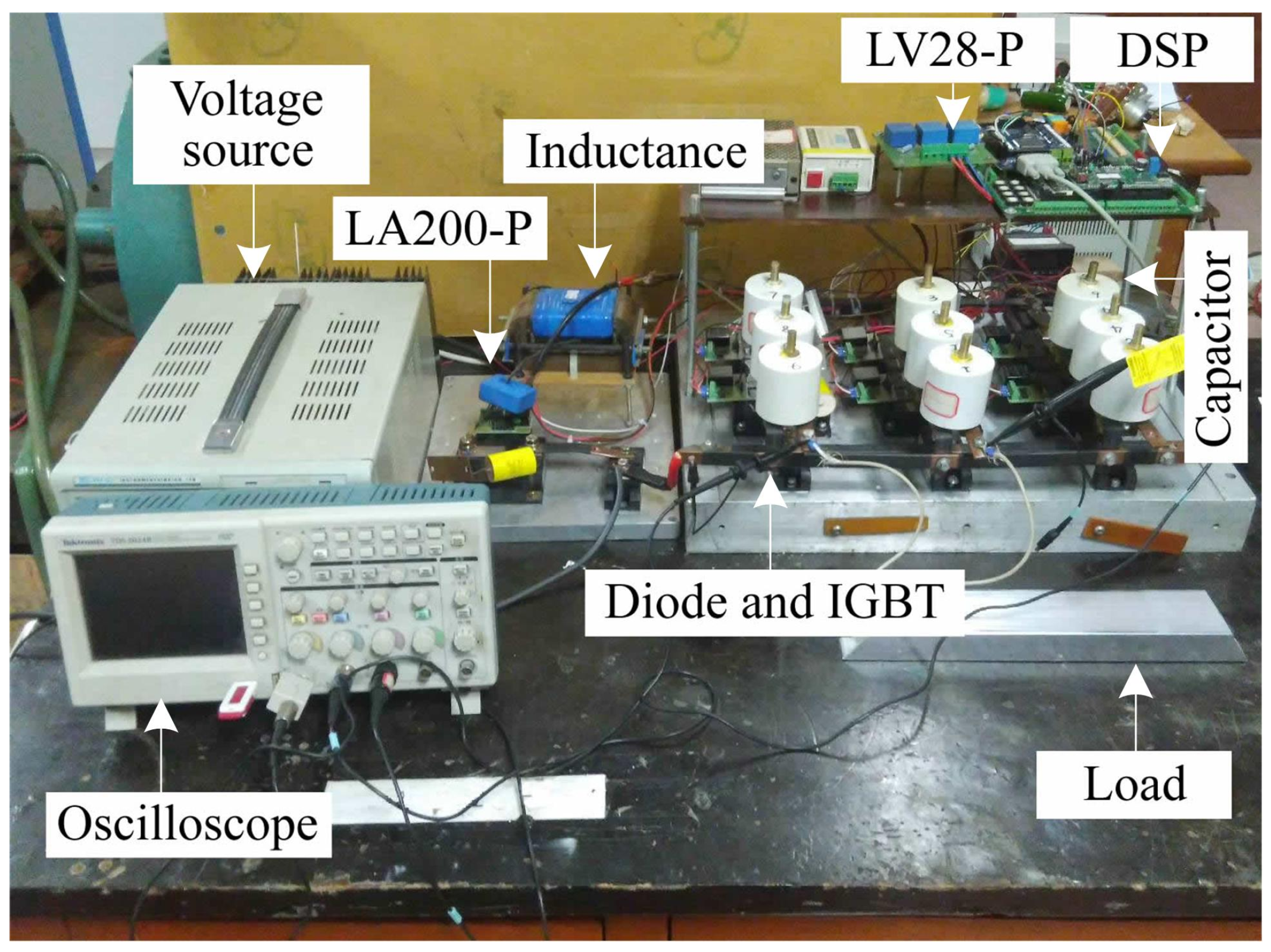
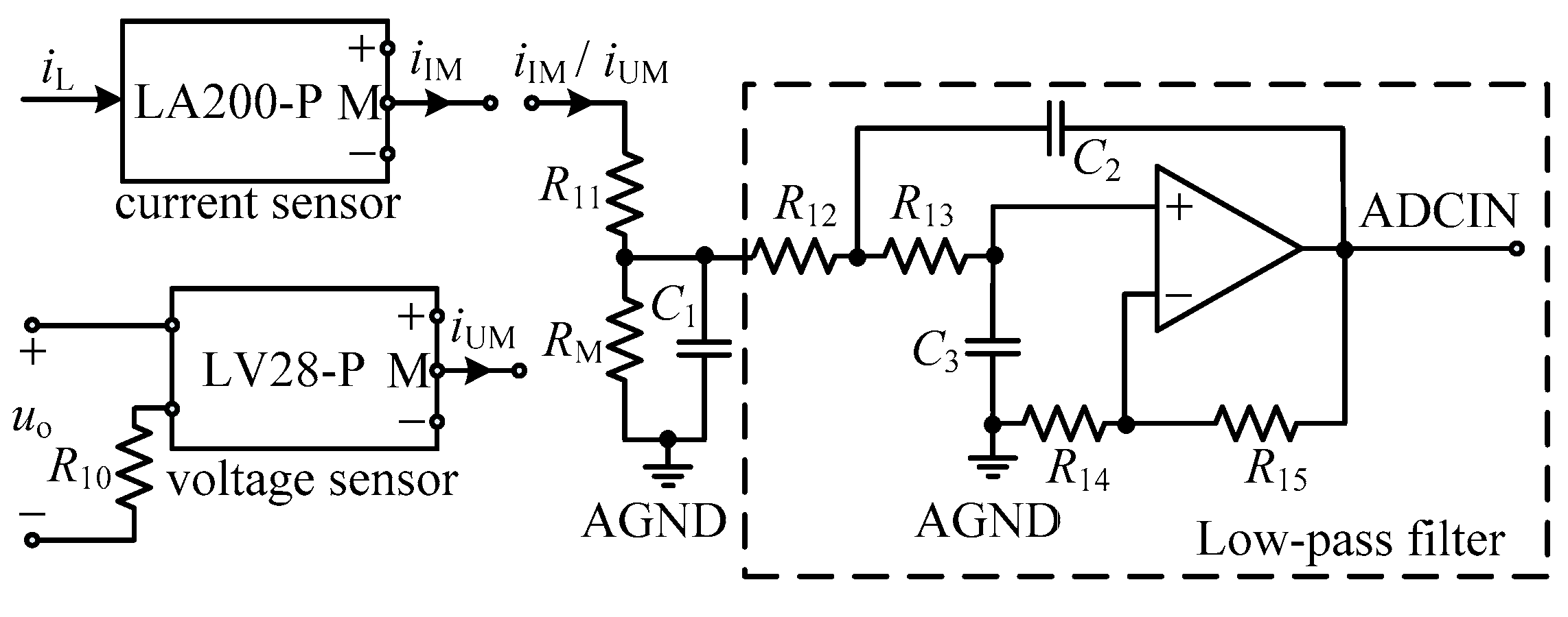
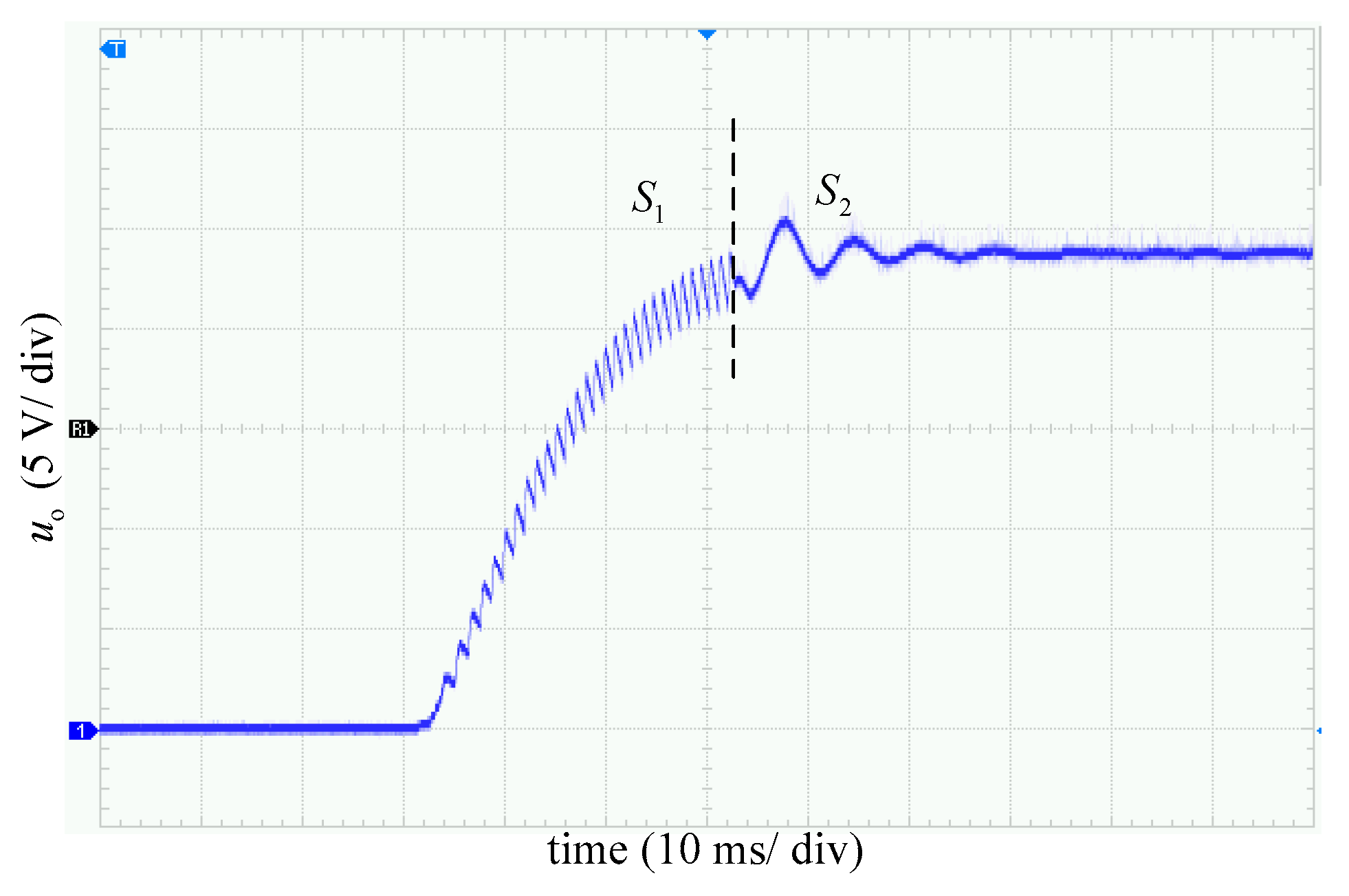
5. Experimental Results
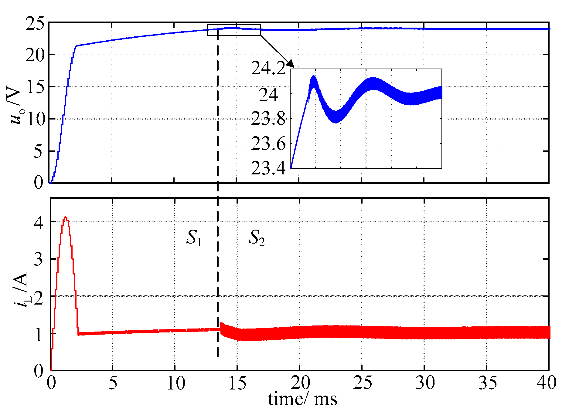
Figure 14 shows the experimental waveform of
uo from the zero initial-state to the steady-state. Compared to the results shown in
Figure 4a, there is no overshoot of
uo in the start-up process under the effect of sliding mode control based on
S1. When
uo first increases to 24 V, sliding mode control based on
S2 is adopted, the transition between switching surface
S1 and
S2 is in an agreement with the simulation results shown in
Figure 8. As shown in this figure, good performance of the boost converter in the start-up process can be obtained by the switching surface
S1. The duration of the start-up is 20 ms and the voltage overshoot is only 4.1%.
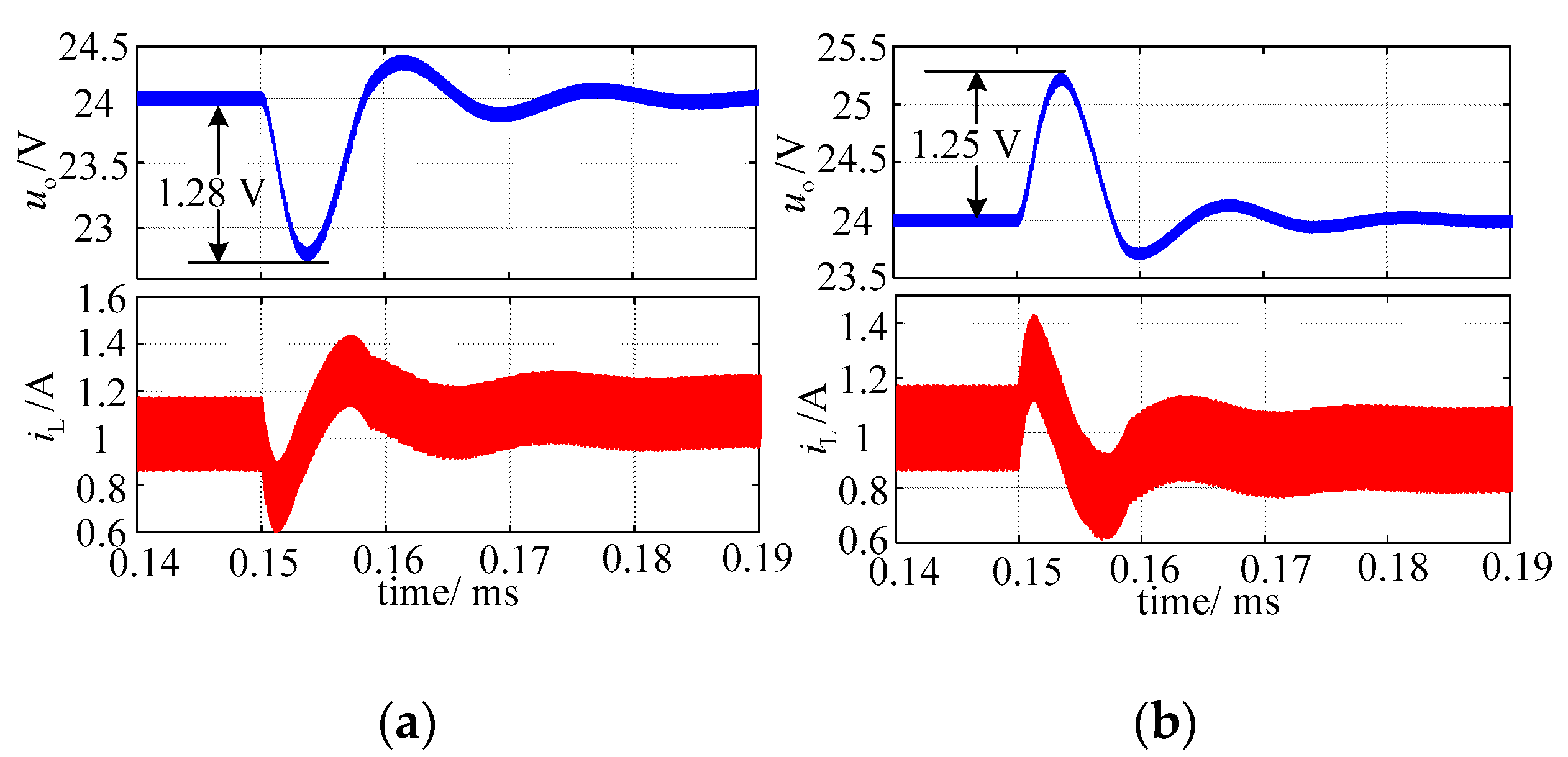
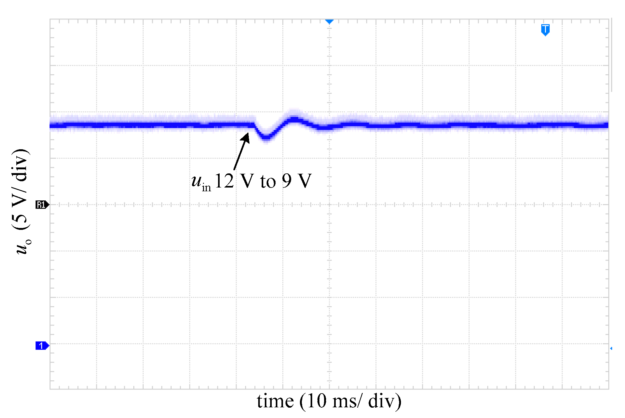
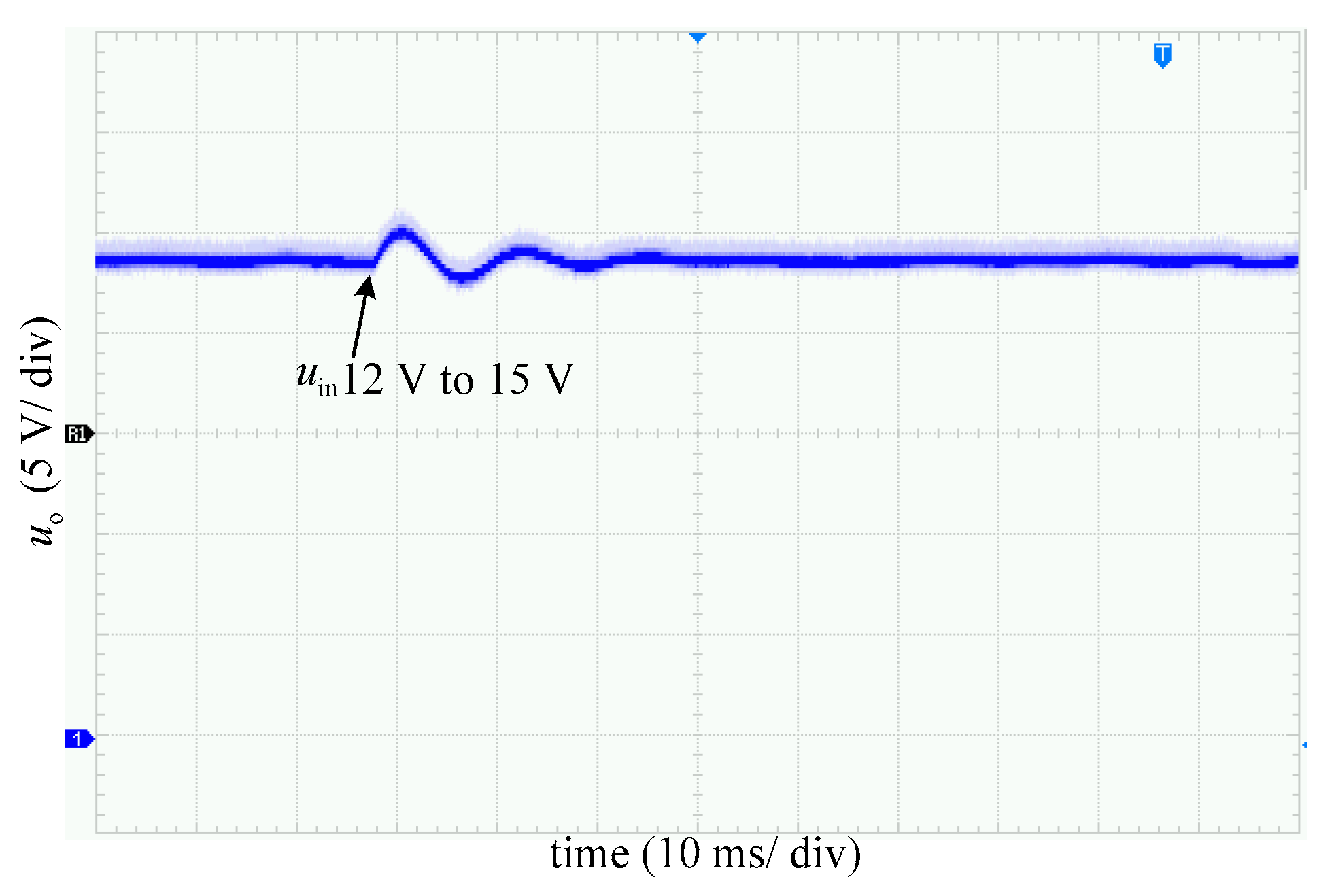
Figure 15 illustrates the experimental response of the input voltage step decreasing from 12 V to 9 V. In contrast,
Figure 16 illustrates the response of the input voltage, increasing from 12 V to 15 V. The experimental results are in good agreement with the simulation results shown in
Figure 9. After ignoring the transient state, the action of the switching surface
S2 can realize a zero steady-state error of
uo. The maximum deviation value is 1.3 V and the dynamic adjustment time is less than 20 ms.
Figure 17 shows the experimental response of the perturbation of load from 40 Ω to 50 Ω and from 50 Ω to 40 Ω respectively. A resistance of 200 Ω series connected with an auxiliary tube is parallel in the nominal load. The perturbation of load is achieved by controlling the auxiliary tube by the switching-on or switching-off state, the switching signal of the auxiliary tube is shown in
Figure 17. Under the action of the switching surface
S2, A zero steady-state error of
uo is also achieved after ignoring the transient state. The maximum deviation value is 2.5 V and the dynamic adjustment time is less than 22 ms. The robustness is proved by simulation and experimental results.
6. Conclusions
For the different conditions of the start-up process and steady-state process of the boost converter, two switching surfaces are proposed in this paper respectively. In the start-up process of the boost converter, switching surface S1, which based on the large-signal model to minimize inrush current, voltage overshoot and adjustment time, is adopted. When the converter operates at a steady-state, the other switching surface S2 including PI compensator is employed to regulate the output voltage, which can suppress the perturbation of input voltage and load fluctuation on the output voltage. Furthermore, the effectiveness of the control strategy proposed in this paper is verified by simulation and experiment. The research results can provide a reference for the engineering design of the sliding mode boost controller, so that the minimum value of the inrush current is compatible with the high voltage regulation value. In electric vehicle applications, the sliding mode control strategy proposed in this paper can be used in a boost converter between the battery and the inverter to suppress battery voltage fluctuations and improve system efficiency.


