Article

One Cycle Control of a PWM Rectifier a New Approach

by
Rodrigo De A. Teixeira
1,†,
Werbet L. A. Silva
1,†,
Guilherme A. P. De C. A. Pessoa
1,†,
Joao T. Carvalho Neto
2,†,
Elmer R. L. Villarreal
3,†,
Andrés O. Salazar
1,*,† and
Alberto S. Lock
4,†
1
Department of Computer Engineering and Automation, Federal University of Rio Grande do Norte (DCA-UFRN), Natal 59072-970, Brazil
2
The Federal Institute of Education, Science and Technology of Rio Grande do Norte (IFRN), Natal 59015-000, Brazil
3
Department of Natural Sciences, Mathematics, and Statistics, Federal Rural University of Semi-Arid (DCME-UFERSA), Mossoro 59625-900, Brazil
4
Renewable and Alternative Energy Center (CEAR-UFPB), João Pessoa, PB 58051-900, Brazil
*
Author to whom correspondence should be addressed.
These authors contributed equally to this work.
Energies 2020, 13(20), 5523; https://doi.org/10.3390/en13205523
Submission received: 1 September 2020 / Revised: 1 October 2020 / Accepted: 3 October 2020 / Published: 21 October 2020
(This article belongs to the Special Issue Power Electronic Converters: Control and Applications)

Abstract

:
This paper analyzes a Digital Signal Processor (DSP) based One Cycle Control (OCC) strategy for a Power Factor Corrector (PFC) rectifier with Common-mode Voltage (CMV) immunity. It is proposed a strategy that utilizes an emulated-resistance-controller in closed-loop configuration to set the dc-link voltage to achieve unity power factor (UPF). It is shown that if the PFC can achieve UPF condition and if the phase voltage is only affected by CMV, then phase current is free from CMV, as well as a lead-lag compensator (LLC) to average phase current.

1. Introduction

One-Cycle Control (OCC)is a nonlinear control theory proposed by [1] able to control switching converters with only one switching cycle. The controller achieves instantaneous dynamic control of an average value of the switching variables after a transient. The most important feature of OCC is the control of the carrier amplitude, in contrast to Pulse Width Modulation, which controls the variable. The OCC technique provides: low complexity, low-cost implementation, disturbance rejection, robustness, good stability and fast dynamic response. OCC based controllers have been widely used to control power factor correction and it has been applied in modular multilevel converters [2], grid-tied single-stage buck-boost DC-AC micro-inverters [3], Vienna Rectifiers [4], novel multi-converter-based unified power quality conditioners (MCB-UPQC) [5] and analysis of harmonics, energy consumption and power quality of light-emitting diode lamps equipped in building lighting systems [6]. The literature also presents a novel, two-stage and hybrid approach based on variational mode decomposition (VMD) and the deep stochastic configuration network (DSCN) for power quality (PQ) disturbances detection and classification in power systems [7]. In the field of power quality, two of the most significant concerns are harmonic currents and power factor (PF) caused by nonlinear loads. While the former may cause false triggering of protection devices and bad functioning of motors and transformers, the later reduces available active power at the utility grid. The past few decades have witnessed extensive studies on power quality, mainly to satisfy specific standards, i.e., IEEE 519-1992 [8], which recommend limiting harmonics distortion. In order to solve these issues for end-consumer, a PWM rectifier can be used to substitute each nonlinear load by an active resistance seen from the utility grid [9]. Hence, this rectifier always tries to achieve unity power factor. If the grid voltage is sinusoidal, then the current drawn by the rectifier must be sinusoidal and in phase with the voltage, avoiding any current harmonics. Several methods have been proposed to achieve UPF in PWM rectifiers based on the enhanced control-loops concept [10], such as: inner current loop, instantaneous power loop and outer voltage loop. To force the phase-current to follow voltage loop reference it is necessary to sense three-phase voltages, a DC-link voltage, three-phase currents [11] and in some cases, the use of a phase-locked loop (PLL) to guarantee voltage and current synchronization [12]. The control techniques based on this concept use space vector modulation (SVM), Park/Clarke transformations and control coupled terms such as: voltage oriented control (VOC) [13], direct power control (DPC) [14], model predictive control (MPC) [15], deadbeat control [16], fuzzy control [17] and neural networks [18]. Nevertheless, these methods are time-consuming, as they rely on system parameters, requiring complicated online calculation. Resistance-emulation is another technique employed in PWM rectifiers, generally using average value and PWM modulators. In this technique is always assumed that UPF is already achieved. There are two main methods based on open-loop and closed-loop controls [9]. Open-loop methods control the estimated emulated-resistance assuming a fixed value [19] while closed-loop methods adjust the emulated-resistance value by feedback [20]. Although these techniques were proposed for single-phase boost converters with diode rectifiers, they are complicated to implement as they employ the four arithmetical operations.
The One Cycle Control is a kind of open-loop method, originally proposed as a hardware technique [21] (Figure 1a) implemented either by a few commercials ICs or just a single chip as a cost-effective solution. It uses a variable sawtooth-carrier-amplitude (Figure 1b) and only adding and subtracting operations, contributing to its arithmetic simplicity and performing its control tasks in the only one switching cycle, therein the name OCC, despite this technique was also proposed for three-phase, six power-switches boost-converter. The OCC technique does not use neither phase-locked-loop (PLL) nor Park/Clarke transformations, which allows a fast dynamic system response while satisfying the UPF condition. Moreover, it eliminates the need of three grid-voltage sensors, which adds control and hardware simplicity. Although this technique was applied several times in active power filters (APF) [22,23], in flexible ac transmission systems (FACTs) [24] and in photovoltaic grid-connected inverters (GCI) [25,26,27], the OCC has presented such serious instability problems [21,28,29]. To solve these issues it was necessary to add extra circuitry sacrificing control and hardware simplicity.
In order to preserve the control and hardware simplicity, the OCC was emulated in a DSP system. A DSP-based software-OCC was proposed in [30] based on the scheme shown on the Figure 1c. This version enhances OCC with DSP calculation capability and uses closed-loop resistance emulation. Then, the software offers more possibilities to apply the OCC to the most complex control issues than those of hardware [31,32,33]. Besides, unlike enhanced-loops methods mentioned above [11,12,13,14,15,16,17,18] The software-OCC does not use PLL, Park/Clarke transformations or online parameter calculations, therefore, it achieves some control simplicity. However, it was not reported any further analysis, in spite DSPs have already applicated to OCC as a control core, i.e., for motor drivers [34,35] and photovoltaics [27], while OCC runs as a sort of auxiliary circuit. Previous treatments to solve stability problems at no-load have sacrificed OCC simplicity once they use an additional bulky resistor at DC-link [21,29]. Instead, in order to decrease current distortion, an artificial phase-current was created [36,37,38]. However, despite the efforts, instability remains when load current falls below a certain limit [24,39,40]. On the other side, due to a lack of PLL synchronization, OCC has experienced PF derating at high-load [21,29,37,38,39]. To avoid this, OCC has sacrificed its simplicity again as they use input voltage multiplexers, and other additional analog and logic circuits [23,24,39,40,41], requiring the knowledge of 600 angular sectors and to select positive and negative peak voltages as reference current vectors. In [28,42], it was also necessary to sacrifice OCC simplicity by adding a few analog multipliers and heavy and bulky inductors (10 mH), but sacrificing the cost-effectiveness of OCC solution. Hence, despite all the efforts, it is apparent that, to date, OCC has been not able, whatsoever, to solve its own problems fully. Above all, even though a few hardware methods have solve partially OCC stability issues at no-load [21,36,37,38,42] and at high-load [28,39,40,41], they were never reported working together over a wide load range. Thus, one of the paper’s major contributions is to present a simple and stable DSP based OCC system working at no-load and high-load considering that the proposed digital implementation presents improvements relationed to hardware-OCC systems. Thus, one of the paper’s major contributions is to present a simple and stable OCC system working at no-load and high-load.
In this paper, analysis, simulation, and experimental results prove, based on the resistance-emulated controller [30], that software-OCC does not possess instability issues and preserves OCC simplicity and dynamical response, also satisfying UPF condition. The paper is organized as follows: Section 2 presents a review of software-OCC fundamentals. Section 3 shows OCC issues and discusses software-OCC solving method. Section 4 depicts DSP implementation and discusses the cost-effectiveness of software-OCC. Simulation and experimental results are shown in Section 5. Conclusions are shown in Section 6.

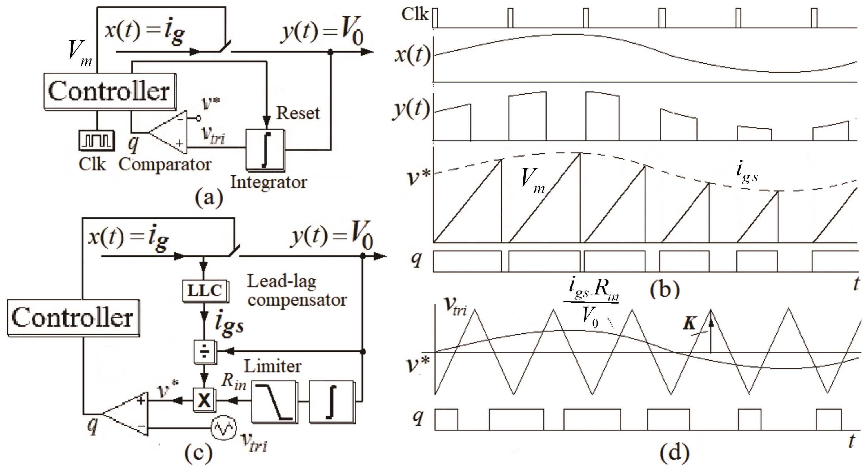
2. Fundamentals of Software-OCC

Software-OCC is a PWM, where an average phase-current compares to carrier and control system is integrated into the modulator, similar to hardware-OCC of (Figure 1c) [21]. Nevertheless, unlike hardware-OCC, this version is not a circuit, but a software. Hence, software-OCC implements OCC features by programming embedded DSP devices and using just a few equations. However, a high-performance OCC system is obtained, as using a high-frequency DSP, the one switching-cycle control can be guaranteed. (Figure 2) displays a three-phase, IGBT PWM rectifier. As in hardware-OCC, it is assumed that,
  • The switching frequency f C is much higher than line frequency f, hence the switching period T C is much lower than the line period T, so f C > > f and T C < < T .
  • The switches in each leg operate in a complementary fashion, i.e., the duty cycle for the upper and bottom switch is d g and d g n = ( 1 d g ) , respectively ( g = a , b , c ), 0 < d g < 1 .
  • Input impedance seen from the grid is a resistance, similar to the resistance emulation concept in [9]. Besides, software-OCC, (Figure 1c), presents the following differences from hardware-OCC.
(i)
Multipliers and dividers presence, as they are not much DSP time-consuming [43].
(ii)
The average method, i.e., a LLC (Figure 1c) decreases the delay response caused by the lagging part, using a leading constant.
(iii)
Carrier generation uses a triangular waveshape, (Figure 1d), instead of a sawtooth carrier in the hardware OCC.
(iv)
Fixed amplitude carrier due of a software DSP limitation.
(v)
Closed-loop emulated resistance-control, guaranteeing UPF by feedback.
(vi)
Use of limiters at resistance control output.
Except for the item (iv), these differences result of the superior software-DSP-calculation capability over hardware technique.
Applying Kirchhoff voltage law to the r L branch in the Figure 2, where r is inductor resistance, L is inductor inductance; v S g and i g are grid voltage and phase current, respectively; v G N is pole voltage ( G = A , B , C ) , O is the middle point of dc-link capacitors C 1 and C 2 , v N O is the voltage between neutral of the utility grid and middle point O of dc-link voltage, and V 0 and I 0 are load voltage and current respectively.
v S a r i a L d i a d t = v A N + v N O v S b r i b L d i b d t = v B N + v N O v S c r i c L d i c d t = v C N + v N O

Analysis of Voltage v N O

The expressions given by (1), it is apparent that to obtain an exact expression for phase-current, it is necessary to find an analytical expression for voltage v N O . However, although some previous works indicate that this voltage does not depend on grid frequency [13,44], the mathematical proof is missing. It is always possible to bypass the problem by assuming some control strategy, as it allows additional simplifications [45,46]. Hence, considering a balanced system:
v S a + v S b + v S c = 0 i a + i b + i c = 0
Grid voltages are given by:
v S a = V p c o s ω t v S b = V p c o s ( ω t 2 π 3 ) v S c = V p c o s ( ω t + 2 π 3 )
where V p is voltage amplitude, V p > 0 . Although OCC does not use references [21,40], for mathematical purposes, it could be useful to admit grid voltage (3), as a virtual phase-current reference, as phase-current has the same waveshape and in phase with of the grid voltages. In addition, considering a balanced system, given by (2), and manipulating (1):
v N O = 1 3 ( v A N + v B N + v C N )
The Equation (4) says that voltage v N O is related to pole voltage. In this way, finding an analytical expression for v N O could be long and tedious as in a PWM modulator, pole voltage depends on Bessel functions and Fourier series [47]. From the Equation (4), the average v N 0 is:
1 T C 0 T C v N O d t = 1 3 T C ( 0 T C v A N d t + 0 T C v B N d t + 0 T C v C N d t )
To find the average pole voltage (Figure 2) it should be noted that:
1 T C 0 T C v G N d t = 1 T C 0 T C v G M d t V 0 2
Since average value of pole voltage v G N over switching period is given by (see Figure 3):
1 T C 0 T C v G N d t = 1 T C [ 0 t g n V 0 d t + t g n T C 0 d t ] = V 0 d g n
where t g n = d g n T C . Hence, combining (6) and (7):
1 T C 0 T C v G N d t = V 0 2 ( 1 2 d g n )
Moreover, as duty cycle in a PWM modulator is proportional to its reference (3), provided that f C > > f [47]:
d g n = D p c o s ( ω t + ϕ )
where 0 < D p < 1 , ϕ is such that, ϕ = 0 for g = a , ϕ = 2 π 3 for g = b and ϕ = 2 π 3 for g = c . Then, combining (5), (8) and (9) yields:
1 T C 0 T C v N O d t = V 0 2
A common assumption in hardware OCC is that the current ripple is small and that inductor current works in current continuous mode, (CCM) [21], so phase-current is proportional to its average value. Thereby, using this assumption in software-OCC, phase-current can be written as:
i g = K T C 0 T C i g ( γ ) d γ
where K is proportionality constant. Then, for t > 0 ,
t d i g ( t ) = K 0 t i g ( γ ) d γ
differentiating former equation:
t d i g d t = ( K 1 ) i g
combining (1) and (13):
v S g r i g L t ( K 1 ) i g = v G N v N O
As input impedance seen from the utility grid is assumed a resistance (condition c):
v S g = R i n 0 i g
where R i n 0 is assumed input resistance seen from the grid. This resistance is based on loss-free resistor concept [48], since it transfers all energy from the input to the output port and does not dissipate active power. Denoting r = ( K 1 ) L t , where K is a constant ( K > 1 ), and combining (14) and (15):
R i n i g = v G N v N O
R i n = R i n 0 ( r + r )
Likewise, resistance R i n is input resistance seen from the grid. Nonetheless, this is the final resistance which is controlled by software-OCC (21) [30,32]. Averaging Equation (16), it leads to:
R i n 1 T C 0 T C i g d t = 1 T C 0 T C v G N d t 1 T C 0 T C v N O d t
Combining the Equations (8), (10) and (18):
R i n i g s = V 0 ( 1 d g n )
where i g s is average phase-current. The right term of the former equation is the variable amplitude of the hardware-OCC carrier. The negative signal means that the carrier comes from V 0 to 0 ( d g n = 1 ).
The former equation is consistent to emulated resistance concept, as that resistance was assumed since operation beginning [9]. Furthermore, this constitutes a classical OCC equation as it achieves the same level of OCC simplicity, i.e., it uses a sawtooth carrier and does not employ coupled terms, nor Park/Clarke transformations [21,40]. In addition, emulated resistance R i n satisfies:
v S g = R i n i g
In order to ensure that resistance is seen from the grid, satisfying condition c, R i n can become a V 0 voltage controller. So if R i n is a V 0 controller, it also controls active power P as it depends on V 0 , since P = V 0 I 0 , where I 0 is load current, Figure 2. Resistance R i n also controls power factor indirectly, since active power (P), reactive power (Q) and apparent power (S) are related by the expression S = P 2 + Q 2 . In this sense, as S is fixed, if power P is set to a relatively high value (close to S), reactive power Q should be close to zero:
R i n = K p ( V 0 V 0 ) + K I ( V 0 V 0 ) d t
where V 0 is load voltage reference, K p , K I are proportional and integrative P I constants, respectively. PI constants are positive K p > 0 , K I > 0 , to guarantee that R i n > 0 , when V 0 > V 0 . R i n controller, name as emulated resistance controller, leads to a resistive impedance seen from the grid. Moreover, in frequency domain R i n controller can be expressed as a function of load voltage error ( V 0 V 0 ) :
R i n = ( V 0 V 0 ) ( K p 1 + K I 1 s )
According to Equation (19), the average current multiplied by R i n is compared to variable amplitude carrier, V 0 A t r i ( t ) , where carrier A t r i ( t ) = ( 1 d g ) . This could be the essence of the OCC method when implemented by hardware since a variable carrier amplitude s a hardware-OCC characteristic [21,36]. However, as the goal of the system is a software implementation, therefore, DSP characteristics must be included. In this order, it would be useful to modify classical software-OCC modulator, (19) to:
q g n = 1 , w h e n i g s . R i n V 0 . A t r i ( t ) 0 , o t h e r w i s e
where q g n is the logical state at the gate of lower switch of power converter shown in Figure 1a. Yet, as DC-link voltage is positive, V 0 > 0 , former relation can be modified as:
q g n = 1 , w h e n ( i g s R i n ) V 0 A t r i ( t ) 0 , o t h e r w i s e
The relationships (23) and (24) are equivalent, once generate the same firing pulses. The relationship represents OCC variable-amplitude carrier Figure 4a while the former is adequate for DSP manipulation, as we willl see later in Section 4. Besides, it resembles a PWM modulator with zero-sequence injection producing Space Vector PWM, (SVPWM [49]), or phase-clamping [50], but without phase-current distortion.

3. Occ Stability Analysis

There is no simple method to analyze hardware-OCC stability by conventional control theory, as this technique is all except conventional, once control and hardware are integrated, while in software-OCC control and hardware are implemented and integrated by software. There are two main stability issues reported in hardware-OCC, at no-load [21,29,36], and high-load [28]. This situations were adressed using a hardware analysis instead of traditional control theory once the OCC instability is provoked by over modulation [21] and hardware limitations and not by poles or zeros misplacement. Stability issues in hardware-OCC can be solved by using an emulated-resistance controller R i n of software-OCC [30] and maximum and minimum limiters (Figure 5). The next subsection presents a model based on emulated-resistance control, which explains the hardware-OCC instability and software-OCC solutions to the problem.

3.1. Hardware-OCC Theoretical Background

In hardware-OCC, voltage V m is a PI controller of DC voltage, given by [21]:
V m = ( V 0 V 0 ) ( K p 1 + K I 1 s )
where V m is the carrier amplitude controller, in frequency domain, V m is defined by [21]:
V m = K 1 R s V 0 R i n 1
where K 1 is a parameter, ( V S g V 0 < K 1 < 1 + V S g V 0 ) ; R S is current sensor resistance ( R S = 1 Ω ) and R i n 1 is emulated resistance [21]. In addition, as in hardware-OCC firing pulses can be defined as:
q g n h = 1 , w h e n i g s v m . A t r i ( t ) 0 , o t h e r w i s e
where q g n h is the logical state at the gate of lower switch of power converter, A t r i h is fixed carrier amplitude. The former equation represents the hardware-OCC modulator since modulating wave is compared to a variable-amplitude carrier, controlled by V m (25). Note that this carrier leads to a multiplication operation, despite OCC arithmetic simplicity. Besides, as for a PWM rectifier, as shown in (Figure 2), average dc voltage V 0 has a voltage ripple V 0 r related to its peak value V 0 p [51], (see Figure 5). Hence
V 0 = V 0 p I 0 8 C T S W
where V 0 r = I 0 8 C , I 0 is the DC-link current; R L is dc-link load; I 0 = V 0 R L ; C the DC-link equivalent capacitor, C = C 1 C 2 ( C 1 + C 2 ) , T S W is switching time period, T S W = 2 T 0 , T 0 is time period between peaks of voltage ripple. Although dc-link capacitor C is assumed large that voltage ripple is neglected and hence average and peak DC-link values are the same [51]. Yet, for practical values of capacitance, only Equation (28) is valid.

3.2. Hardware-OCC Issues

In principle the control technique with hardware-OCC offers a simple solution in terms of hardware, control and arithmetic, however, every system connected to the network needs synchronization, and the lack of synchronization may result in instability and power factor reduction. In order to overcome this situation, the carrier with variable amplitude was created, but at the cost of instability in the system without load.
Stability at no-load: in general in a PWM rectifier the output power P 0 equals input power P T minus power losses, P L , ( P 0 = P T P L ). Then, admitting a proportionality factor ( K 3 ) between power losses and input power:
P 0 = K 3 P T
In addition, assuming UPF, input power is given by:
P T = 3 V S g I g
where V S g and I g denotes grid voltage and phase current in frequency domain, respectively, while the output is:
P 0 = V 0 I 0
Then, combining Equations (29)–(31), it yields:
I g = K 4 I 0
where ( K 4 = V 0 ( 3 K 3 V S g ) ) and I 0 is the DC current. The former equation says that phase-current I g is proportional to I 0 . Yet, Equation (32) has practical limits given by the sensitivity of the technique. A small phase-current could exist when I 0 is null, or lower than a threshold value, I 0 t h , causing phase-current distortion when I g is greater than amplitude V m , as reported in [21,24,29,36,37,38,39,40]. In order to explain this phenomenon from an emulated-resistance approach, the Equation (26) can be rewritten as:
R i n 1 = K 1 V 0 V m
Which leads to a virtual input resistance R i n 1 , as a sort of V 0 controller. Besides, as in OCC, phase-current varies according to [52]:
I g = V S g R e + s L
where R e denotes the OCC input resistance in frequency domain. Hence, by making R e = R i n 1 and combining Equations (25), (33) and (34):
m a = I g V m = V S g K 1 V 0 + L ( V 0 V 0 ) ( s K P 1 + K I 1 )
The Equation (35) denotes the modulation index m a , as I g is the phase current in the frequency domain and V m is carrier amplitude [21]. Applying the final value theorem to Equation (35), for a unit step response ( 1 s ) :
m a = l i m S 0 1 S S I g V m = V S g K 1 V 0 + L K I ( V 0 V 0 )
Due to the increase of V 0 without load, it tends to its reference V 0 , while V 0 V 0 approaches zero. In this case, Equation (36) becomes:
m a = V S g K 1 V 0
The overmodulation occurs when m a > 1 Equation (37) as V p V 0 > K 1 > 0 , once ( V S g = V p c o s ω t ) , Equation (3), m a > 0 , K 1 = 0.25 V p V 0 , m a = 4 , V p > 0 , V 0 > 0 . The Equation (37) can explain why previous works did not suppress fully the overmodulation by growing or falling the I g [24,36,37,38,39,40], once K 1 cannot be controlled [21]. The Figure 6 illustrates this by ploting m a vs. K 1 , Equation (37), for 0.67 > K 1 > 0.19 , V p = 155.56 V, V 0 = 467 V, when I g grows 20 % (A) and when I g falls 20 % (C). Notice that when K 1 0.25 , the method does not work, as m a > 1 .
As was mentioned earlier, PF derating occurs through a lack of grid synchronization. However, this can not be predicted by an open-loop resistance-emulator value, r e [12,21] as in frequency domain it leads to R e = r e s , which combined to Equation (34), it gives I g = s V S g ( r e + s 2 L ) , leading to an admittance angle ϕ v = a r c t a n ( I g V S g ) = π 2 . However, a better prediction can be obtained by combining Equations (25) and (35):
I g V S g = ( V 0 V 0 ) ( s K P 1 + K I 1 ) [ s K P 1 L ( V 0 V 0 ) + K I 1 L ( V 0 V 0 ) + K 1 V 0 ] s
Therefore, the phase angle ϕ v is given by:
ϕ v = ϕ 1 a r c t a n [ ω L K P 1 ( 8 C ( V 0 V 0 p ) + I 0 T S W ) L K I 1 ( 8 C ( V 0 V 0 p ) + I 0 T S W ) + K 1 ( 8 C V 0 p + I 0 T S W ) ]
ϕ I 0 = 8 ω L C T S W K P 1 K 1 V 0 ( L K I 1 I 0 T S W + K 1 ( 8 C V 0 p I 0 T S W ) ) 2 + ( ω L K P 1 I 0 T S W ) 2
It can be noticed that the former equation predicts PF derating because admittance angle ϕ v is a decreasing function. It matches the results of previous works [29,37,38,39]. The Figure 7 shows Equation (39), V p = 155.56 V, V 0 p = V 0 = 467 V, K 1 = 1 , K p 1 = 1 , K I 1 = 1 . The figure confirms that ϕ v is decreasing when I 0 increases, from I 0 = 10 A (P) to I 0 = 20 A (N) and I 0 = 30 A (M).

3.3. Software-OCC Solutions

Although subtle, the main difference between Hardware-OCC and Software-OCC is in bus voltage control, in the hardware version this controller is called V m and controls the amplitude of the carrier Equations (25) and (27), in the software version this controller is called R i n and controls modulation. However, only R i n allows the OCC to solve instability problems and power factor decrease.
As was mentioned earlier, phase-current is proportional to DC current, Equation (32), but only under practical limits, through the sensitivity of OCC modulator. Since a small distorted phase-current could appear when DC current is less than the threshold current, I 0 t h . In order to avoid this effect in software-OCC, maximum the controller limiter R i n m a x could be calibrated to set up minimum phase-current I g m i n , since I g = V S g R i n , Equation (20). Then, as voltage V S g is fixed, minimum phase-current I g m i n occurs when the resistance R i n m a x is reached, as I g R i n = V S g is a hyperbolic curve working at first quadrant, I g > 0 , R i n > 0 . That is:
I g m i n = V S g R i n m a x
Thereby, to avoid phase-current distortion at no-load, R i n m a x must be set up to achieve a minimum phase-current I g m i n when DC current is less than I 0 t h . Thus:
I g = I g m i n , w h e n I 0 < I 0 t h K 4 I 0 , w h e n I 0 I 0 t h
Figure 8 shows a plot of I g vs. I 0 , Equation (32), when I g m i n = 1.4 A, I 0 t h = 0.5 A, v S g = 110 V, R i n m a x = 78.01 Ω . Unlike hardware-OCC, a tiny DC controller value does not provoke overmodulation, so the current distortion becomes simpler to avoid. As at no-load, there is no current distortion, it would be necessary to check if at no-load PF derating could be generated. In this sense, no-load and high-load cases must be analyzed for PF derating. Thus, substituting R e = R i n in Equation (34):
I g = V S g R i n + s L
Note that in the former equation if denominator left term is much greater than the right one, ( R i n > > s L ) on this way, the last equation becomes equivalent to Equation (20). However, to achieve UPF, another expression can be found by combining Equations (22) and (43), and relation ( R i n > > s L ) :
I g = V S g ( V 0 V 0 ) ( K P + K I s )
The Relation ( R i n > > s L ) can be forced by setting resistance lower limit R i n m i n = 10 ω L , as showed in Figure 5, since in practice this relation implies ( R i n 10 ω L R i n 10 ω L ) . Besides, from the Expression (44), admittance angle ( ϕ = a r c t a n ( I g V S g ) ) is given by:
ϕ v = π 2 a r c t a n ( ω K P K I )
It can be noticed that this angle does not depend on the DC current, nor dc voltage. Figure 9 shows a plot of admittance angle ϕ v vs. ω , for the software-OCC, Equation (45), when K P = 1 and K I = 1 . This plot does not depend on the DC current.

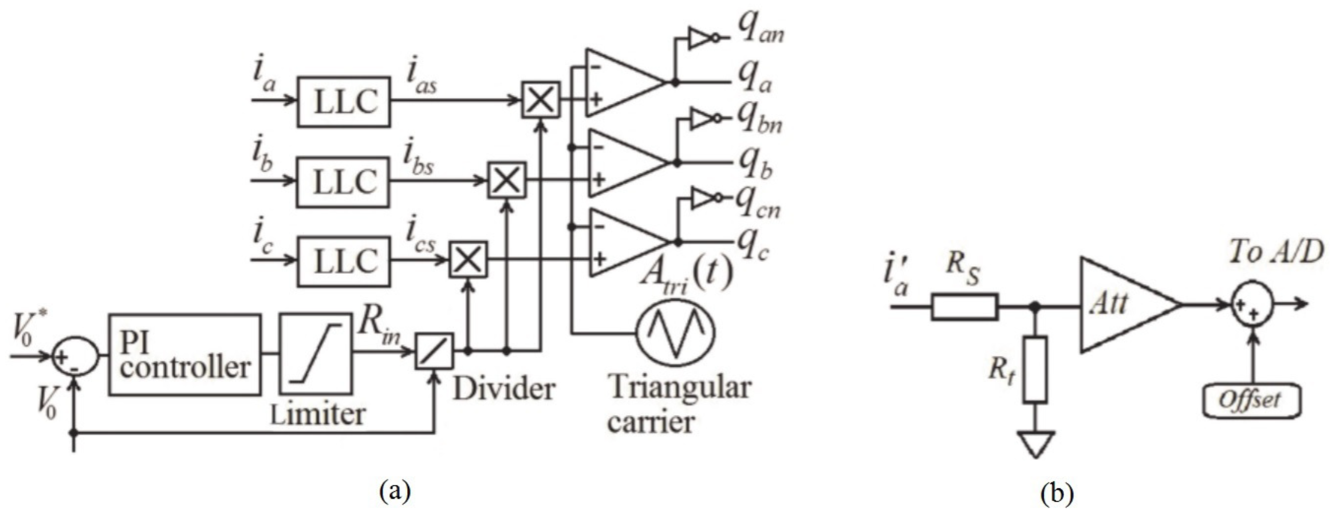
4. DSP Implementation

As can be observed in Figure 10a, Software-OCC controller employs embedded DSP devices like PWM modulators, analog to digital converters and the arithmetic-logic unit, blocks to perform all its tasks digitally, arithmetic and logic operations (including multiplication and division), digital comparators, digital inverters, PI controllers, output limiters and lead-lag compensators (LLC). Yet, it is necessary a phase-current conditioner. As observed in the Figure 10b, it is necessary a phase-current conditioner consisting of a Hall-effect current-sensor [53], some operational amplifiers, OP-AMPs, and a few resistors to change phase-current over dc voltage and then transforms it into digital, through A/D converter.
Hence, a proportionality between analog and digital is guaranteed for DSP to perform OCC control operations, once a scale factor K S (bits /A) is maintained for all currents. For hardware-OCC, something similar occurs, but now the scale factor is a resistance R S (V/A), since a current-sensor resistor is generally used in hardware systems. Anyway, for the sake of simplicity, to establish an equivalency between hardware and software-OCC, it is defined in the later, resistor R S as unity, R S = 1 Ω , denoting that phase-current corresponds to the digital value adopted in DSP control operations. After the digitalizing process, phase-current pass through the software implemented LLC, which averages phase-current according to:
F ( s ) = G 0 ( 1 + s τ 1 ) ( 1 + s τ 2 )
where ( F ( s ) = I g s ( s ) I g ( s ) ) , and I g s ( s ) and I g ( s ) correspond in the frequency domain to the phase current and its average respectively, in the time domain G 0 is the gain, and τ 1 , τ 2 are lead and lag compensator constants. The main idea of the former equation is to average the phase-current i g without unwanted delay on phase angle, from the manipulation of τ 1 and τ 2 values. A further analysis of LLC on software-OCC is performed in [32]. On the other hand, for DSP, carrier waveshape (a sawtooth or a symmetrical triangle) is a choice of DSP-PWM modulator. Thus, in software-OCC, a triangle carrier is chosen since, for a sinusoidal modulating wave, it produces less current harmonics than those in a sawtooth carrier [54]. Another DSP choice is produced when carrier slope (rising or falling) intercepts current, generating an inherent delay related to the inverse of the carrier frequency. This does not jeopardize the time control algorithm, as DSP operations are performed between the interceptions. Yet, in software-OCC, a variation in carrier amplitude also involves a variation in carrier frequency, as shown in Table 1 [55]. Then, there is no direct method to change carrier amplitude without vary carrier frequency also. However, in order to solve this issue, focusing on generating the same firing pulses, the OCC modulator (Equation (23)) is modified as in the Equation (24), which becomes the most suitable expression for DSP implementation as it considers a fixed carrier amplitude. In fact, the software-OCC controller is based on Equations (21) and (24), as observed in Figure 10.

Cost-Effectiveness Software-OCC Discussion

Although the solution with Hardware-OCC is a cost effective solution [21], it presented serious stability problems, which was not practical for applications like APF [56] and photovoltaic systems [27]. Later instability solutions performed by hardware at no-load were reported, but there was always current distortion when dc current falls below a certain level [24,36,37,38,39,40], except when a bulky resistor was placed at dc-link [21,29] and at high-load where complex circuits [23,24,39,40,41], or costly systems were used [28,42]. Thereby, despite these works represent a nice try to solve specific problems, they do not provide a definitive solution, even sacrificing hardware simplicity, or cost-effectiveness of OCC [21,29]. Furthermore, any of the above-mentioned reported works were capable of operating both at no-load and at high-load. Thus, to compare the fair cost-effectiveness of existing hardware-OCC works with present software-OCC, it would be necessary to compare reported works of the same performance, that is, OCC rectifiers operating at a wide range of load. Otherwise, it is like comparing a calculator with a computer. Above all, although the present work was implemented by using a TMS 320 F 28335 evaluation board in a laboratory prototype, a pretty cost-effective solution could be found acquiring a DSP chip and its accessories separately, or by using a simpler DSP, or a microcontroller chip, i.e., a PIC. In any case, the present proposal results in a cost-effective solution on a full range of load, at least, for lack of another option.

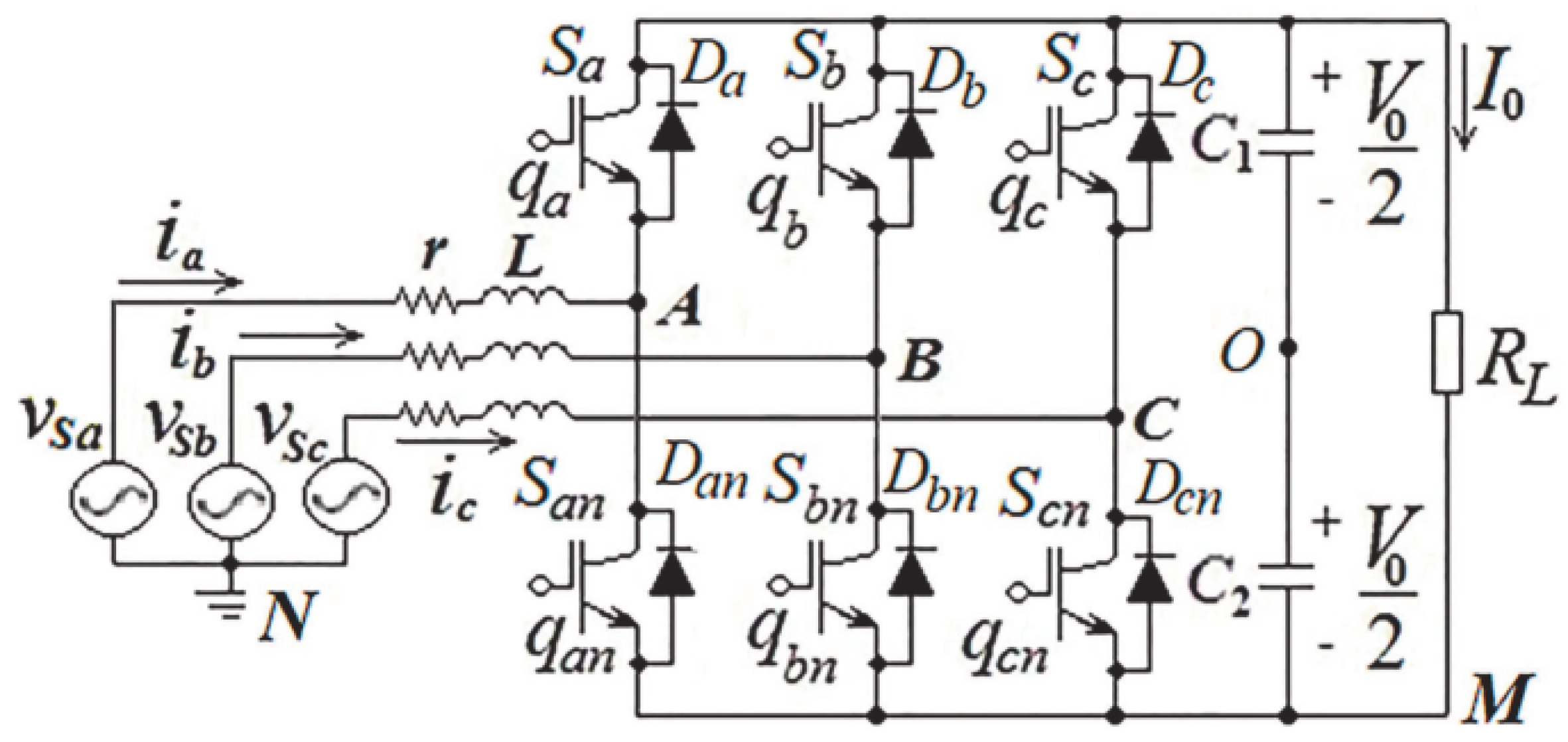
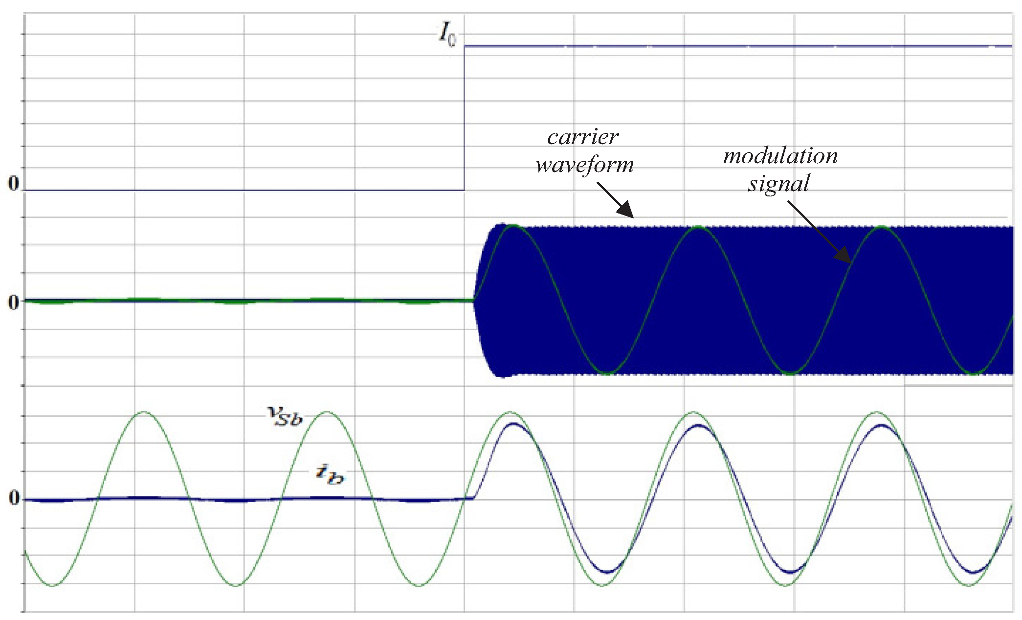
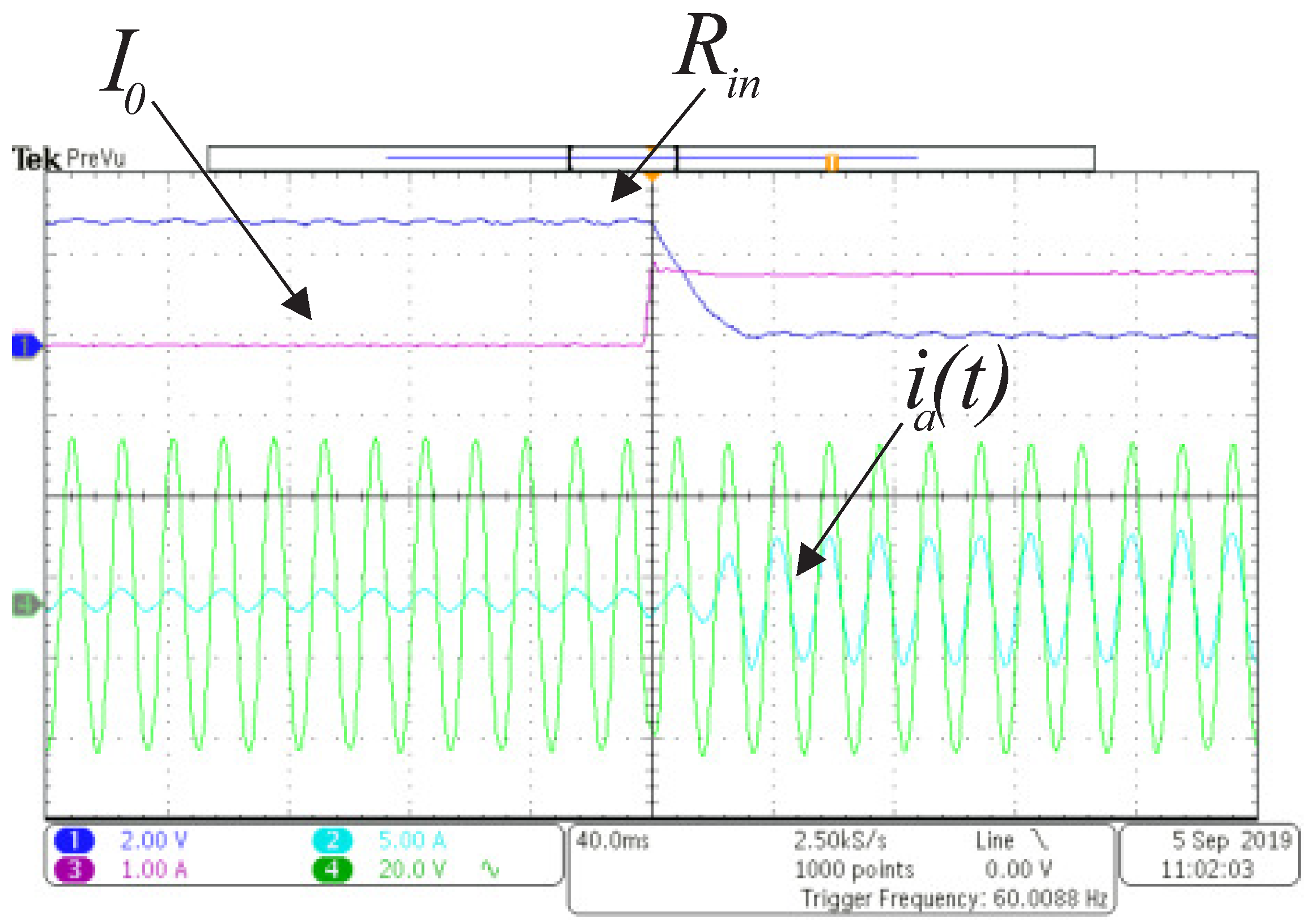
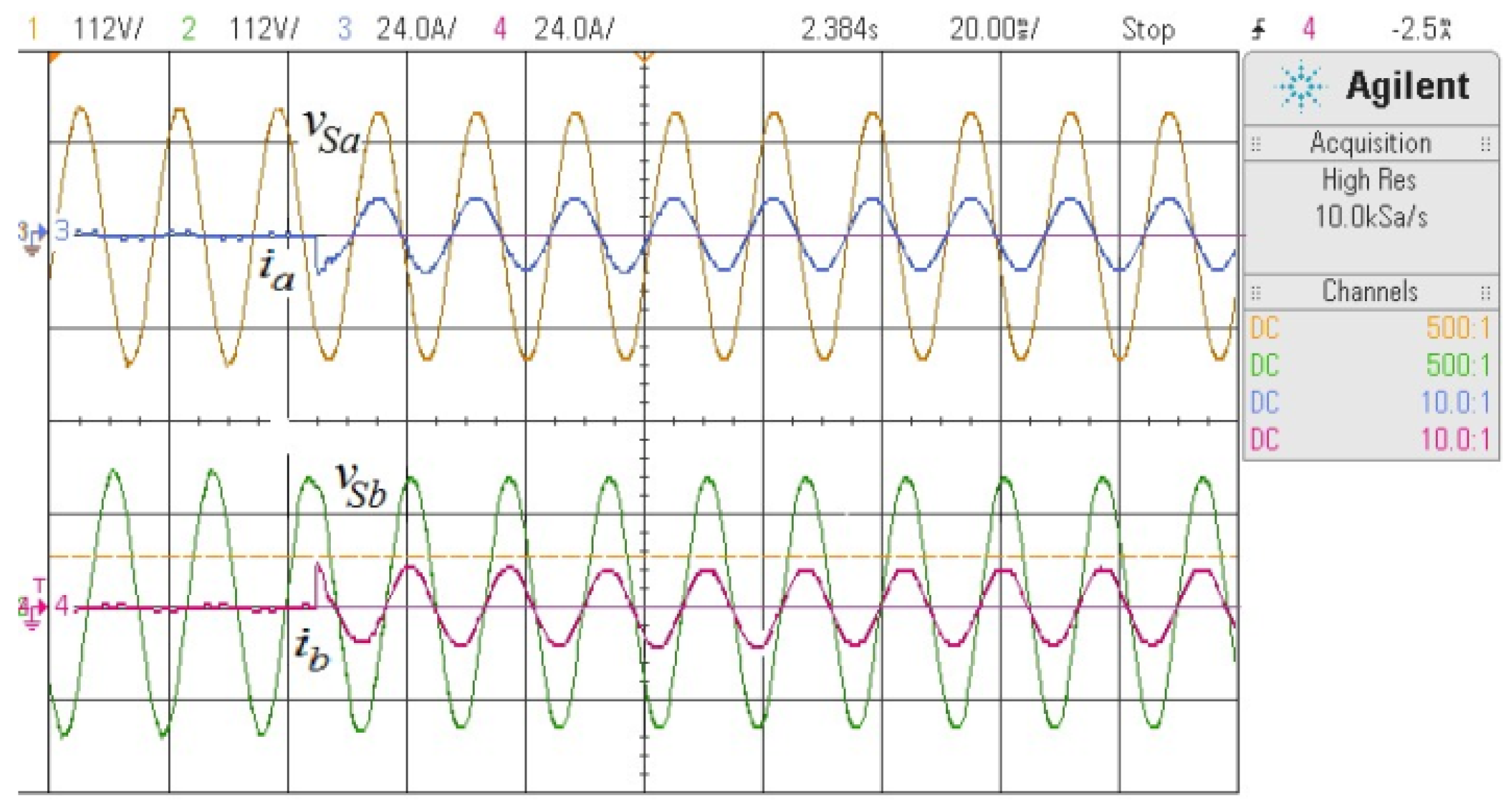
5. Simulation and Experimental Results

The performance of software-OCC has been verified by simulation by using MATLAB and PSCAD/EMTDC and by experimental runs using DSP TMS320F28335. The experiments were performed in a three-phase rectifier similar to the one shown on the Figure 11. The simulation results from PSCAD software are shown in the Figure 12, Figure 13 and Figure 14. The MATLAB ones are shown in the Figure 7 and Figure 9. From the Figure 15, Figure 16, Figure 17, Figure 18, Figure 19, Figure 20, Figure 21, Figure 22, Figure 23, Figure 24 and Figure 25 we show the experimental results.
Parameter values are in Table 2. In Figure 21 and Figure 26, V g r m s = 110 V and V 0 = 100 V, but in Figure 15, Figure 16, Figure 17, Figure 18, Figure 19 and Figure 20, due to technical problems, V g r m s = 21 V and V 0 = 100 V. Figure 12 presents a simulation result only with hardware-OCC evidencing its instability, while the Figure 26 presents a simulation result on stability at no-load and high-load conditions for software-OCC. It can be observed that at no-load, it does not present hardware-OCC stability issues, like overmodulation [21] (current distortion), nor present PF derating. This result verify Equation (43) when K P 1 > > K I 1 .
Experimental results in Figure 15, Figure 16, Figure 17, Figure 18, Figure 19, Figure 20, Figure 21, Figure 22, Figure 23 and Figure 24 are dedicated to confirm former result, or enhance it. Figure 26 shows software-OCC behavior at start-up at no-load, verifying that there is no current distortion, unlike [21], nor even in smaller amount [36,37,38]. This is because to avoid current distortion, software-OCC can define minimum current when load current is null, by using R i n . Figure 15 illustrates dc-link voltage response to a current step, from no-load to high-load, showing a relatively fast-software-OCC dynamic-response considering dc-link capacitors size, thus complementing the Figure 12, Figure 13 and Figure 14. Figure 16 is the enlargement of Figure 15 highlighting the rapid dynamics of the system. Figure 15 shows the dynamics of the emulated resistor R i n due to load variation in the rectifier circuit.
It can be noticed in the Figure 26, that at no-load, when I 0 = 0 , phase-current is small, but it does not exhibit current distortion, as it could be expected considering power balancing in Equation (41), but instead, regarding a minimum phase-current, according to Equation (42), see Figure 16, Figure 17 and Figure 19. Also, it can be observed that there is no power factor derating, as occurs in conventional hardware-OCC [21], (see Figure 18 and Figure 20), and to preserve power factor, it is not necessary to use bulky inductors, unlike [28,42], as observed in Table. Table 2. Thus, also confirming the Figure 26.
From Figure 17 and Figure 19, it can be deduced that the present proposal satisfies IEEE Std 519-1992 [8], as current distortion is small. The Figure 18 shows the proposed controller start-up when the load is high. It illustrates a high dynamic response of software-OCC at high-load and that in such conditions there is no PF derating. This result could substitute Figure 16 and Figure 23 results, once these figures do not achieve high-load results. On the other hand, the Figure 20 shows PF derating vs. phase current at different load conditions. Figure 20 demonstrates that there is a tiny variation when phase currents change. Figure 21 and Figure 22 illustrate DC-link voltage response to a current step, from high-load to no-load, showing a relatively fast software-OCC dynamic-response due to DC-link capacitors size, thus complementing the Figure 26. Figure 23 illustrate the current variation at the output of the rectifier I 0 and the resistance R i n .
Figure 24 illustrates the dynamic response of software PWM-OCC (switching frequency: 24 kHz, R L : 100 Ω ) as well as the charging capacitor of the dc-link voltage. It spends approximately 0.55 s, which is consistent with C = 1100 μ F, Table 2, and R L . The time constant τ = R L C and charging capacitor should last 3 τ approx. Although OCC systems usually have a high dynamic response, for DC-link capacitor charging, this response depends on the capacitor value. In the present case, the capacitor value could not be changed due to the physical stability of the Semikron board and laboratory facilities setup Figure 25.

6. Conclusions

Despite the stability problems, the hardware-OCC contributions to power quality like hardware and control simplicity and high dynamic response are well known. Somehow, software-OCC raises as a solution to these problems and as a way to enhance and increase OCC contributions. The DSP can not emulate variable-carrier amplitude OCC in this software version, since switching frequency depends on the carrier amplitude and vice versa. However, using a mathematical equivalency, the firing gate pulses of the software-OCC and the hardware-OCC are equivalent. This allows the resistance controller limiters to solve stability issues.
From the stability analysis of the emulated-resistance controller for a PWM rectifier, it has stated that: despite, several authors provided solutions to hardware-OCC instability at no-load, or at high-load separately; any of these provide a full-load solution, at no-load and at high-load at the same time. The Software-OCC does not present Hardware-OCC problems, even over a wide load range, and presents a cost-effective solution, once DSP and its components were acquired separately, or a simpler DSP or a PIC was acquired. The Software-OCC also provided fast dynamic-response in comparison to the researches in this field, eliminating power factor derating and minimizing current distortion caused by overmodulation.

Author Contributions

A.O.S. and A.S.L. conceived and designed the study; J.T.C.N., methodology; R.D.A.T., G.A.P.D.C.A.P. and W.L.A.S. performed the simulations and experiments; J.T.C.N. and A.S.L. reviewed the manuscript and provided valuable suggestions; E.R.L.V. and A.L. wrote the paper; supervision, A.O.S. All authors have read and agreed to the published version of the manuscript.

Funding

This research was funded in part by the Coordenacao de Aperfeicoamento de Pessoal de Nivel Superior-Brasil (CAPES)-Finance Code 001 and Conselho Nacional de Desenvolvimento Cientifico e Tecnologico (CNPq).

Conflicts of Interest

The authors declare no conflict of interest.

Abbreviations

The following abbreviations are used in this manuscript:
DSPDigital Signal Processor
OCCOne Cycle Control
CMVCommon-mode Voltage
LLClead-lag compensator
UPFunity power factor
APFactive power filters
FACTsflexible ac transmission systems
GCIphoto-voltaic grid-connected inverters.

References

  1. Smedley, K.M.; Cuk, S. One-cycle control of switching converte. In Proceedings of the 22nd Annual IEEE Power Electronics Specialists Conference (PESC ’91), Cambridge, UK, 24–27 June 1991; pp. 888–896. [Google Scholar]
  2. Zhao, B.; Huangfu, Y.; Abramovitz, A. Derivation of OCC Modulator for Grid-Tied Single-Stage Buck-Boost Inverter Operating in the Discontinuous Conduction Mode. Energies 2020, 13, 3168. [Google Scholar] [CrossRef]
  3. Tian, X.; Ma, Y.; Yu, J.; Wang, C.; Cheng, H. A Modified One-Cycle-Control Method for Modular Multilevel Converters. Energies 2019, 12, 157. [Google Scholar] [CrossRef] [Green Version]
  4. Wang, C.; Liu, J.; Cheng, H.; Zhuang, Y.; Zhao, Z. A Modified One-Cycle Control for Vienna Rectifiers with Functionality of Input Power Factor Regulation and Input Current Distortion Mitigation. Energies 2019, 12, 3375. [Google Scholar] [CrossRef] [Green Version]
  5. Yang, B.; Liu, K.; Zhang, S.; Zhao, J. Design and Implementation of Novel Multi-Converter-Based Unified Power Quality Conditioner for Low-Voltage High-Current Distribution System. Energies 2018, 11, 3150. [Google Scholar] [CrossRef] [Green Version]
  6. Phannil, N.; Jettanasen, C.; Ngaopitakkul, A. Harmonics and Reduction of Energy Consumption in Lighting Systems by Using LED Lamps. Energies 2018, 11, 3169. [Google Scholar] [CrossRef] [Green Version]
  7. Cai, K.; Alalibo, B.P.; Cao, W.; Liu, Z.; Wang, Z.; Li, G. Hybrid Approach for Detecting and Classifying Power Quality Disturbances Based on the Variational Mode Decomposition and Deep Stochastic Configuration Network. Energies 2018, 11, 3040. [Google Scholar] [CrossRef] [Green Version]
  8. IEEE Standard 519-1992. Recommended Practice and Requirements for Harmonic Control in Electric Power Systems; IEEE: Piscataway, NJ, USA, 1992. [Google Scholar]
  9. Erickson, R.W. Fundamentals of Power Electronics; Kluwer Academic Publishers: Dordrecht, The Netherlands, 2000. [Google Scholar]
  10. Rodriguez, J.R.; Dixon, J.W.; Espinoza, J.R.; Pontt, J.; Lezana, P. PWM regenerative rectifiers: State of the art. IEEE Trans. Ind. Electron. 2005, 52, 5–22. [Google Scholar] [CrossRef]
  11. Hartman, M.; Ertl, H.; Kolar, J.W. Current control of three phase rectifier system using three independent current controllers. IEEE Trans. Power Electron. 2013, 28, 2088–3000. [Google Scholar] [CrossRef]
  12. Chung, S.K. Phase-locked loop for grid-connected three-phase power conversion systems. IEE Proc.-Electr. Power Appl. 2000, 147, 213–219. [Google Scholar] [CrossRef]
  13. Kazmierkowski, M.; Malesani, L. Current control techniques for three-phase voltage-source PWM converters: A survey. IEEE Trans. Ind. Electron. 1998, 45, 691–703. [Google Scholar] [CrossRef]
  14. Monfared, M.; Rastegar, H.; Kojabadi, H.M. High performance direct instantaneous power control of PWM rectifiers. Energy Convers. Manag. 2010, 51, 947–954. [Google Scholar] [CrossRef]
  15. Bouafia, A.; Gaubert, J.; Krim, F. Design and implementation of predictive current control of three-phase PWM rectifier using space-vector modulation (SVM). Energy Convers. Manag. 2010, 51, 2473–2481. [Google Scholar] [CrossRef]
  16. Malesani, L.; Mattavelli, P.; Buso, S. Robust dead-beat current control for PWM rectifier and active filters. IEEE Trans. Ind. Appl. 1999, 35, 613–620. [Google Scholar] [CrossRef]
  17. Dixon, J.; Contardo, J.; Moran, L. A Fuzzy-Controlled Active Front-End Rectifier with Current Harmonic Filtering Characteristics and Minimum Sensing Variables. IEEE Trans. Power Electron. 1999, 14, 724–729. [Google Scholar] [CrossRef]
  18. Coteli, R.; Acikgoz, H.; Ucar, F.; Dandil, B. Design and implementation of Type-2 fuzzy neural system controller for PWM rectifiers. Int. J. Hydrogen Energy 2017, 42, 20759–20771. [Google Scholar] [CrossRef]
  19. Chattopadhyay, S.; Ramanarayanan, V. Digital Implementation of a Line Current Shaping Algorithm for Three Phase High Power Factor Boost Rectifier Without Input Voltage Sensing. IEEE Trans. Power Electron. 2004, 19, 709–711. [Google Scholar] [CrossRef] [Green Version]
  20. Maksimovic, D.; Jang, Y.; Erickson, R.W. Nonlinear-carrier control for high-power-factor boost rectifiers. IEEE Trans. Power Electron. 1996, 11, 578–584. [Google Scholar] [CrossRef]
  21. Qiao, C.; Smedley, K.M. Unified constant-frequency integration control of three-phase standard bridge boost rectifiers with power-factor correction. IEEE Trans. Ind. Electron. 2003, 50, 100–107. [Google Scholar] [CrossRef]
  22. Qiao, C.; Smedley, K.M. Three-Phase Bipolar Mode Active Power Filters. IEEE Trans. Ind. Appl. 2002, 38, 149–158. [Google Scholar] [CrossRef]
  23. Qiao, C.; Jin, T.; Smedley, K.M. One-cycle control of three-phase active power filter with vector operation. IEEE Trans. Ind. Electron. 2004, 51, 455–463. [Google Scholar] [CrossRef]
  24. Jin, T.; Li, L.; Smedley, K.M. A Universal Vector Controller for Four-Quadrant Three-Phase Power Converters. IEEE Trans. Circuits Syst. Regul. Pap. 2007, 54, 377–390. [Google Scholar] [CrossRef]
  25. Chen, Y.; Smedley, K.M. A cost-effective single-stage inverter with maximum power point tracking. IEEE Trans. Power Electron. 2004, 45, 1289–1294. [Google Scholar] [CrossRef]
  26. Chen, Y.; Smedley, K.M. Three-Phase Boost-Type Grid-Connected Inverter. IEEE Trans. Power Electron. 2008, 23, 2301–2309. [Google Scholar] [CrossRef]
  27. Fortunato, M.; Giustiniani, A.; Petrone, G.; Spagnuolo, G.; Vitelli, M. Maximum Power Point Tracking in a One-Cycle-Controlled Single-Stage Photovoltaic Inverter. IEEE Trans. Ind. Electron. 2008, 55, 2684–2693. [Google Scholar] [CrossRef]
  28. Ghodke, D.V.; Sreeraj, E.S.; Chatterjee, K.; Fernandes, B.G. One-Cycle-Controlled Bidirectional AC-to-DC Converter with Constant Power Factor. IEEE Trans. Ind. Electron. 2009, 56, 1499–1519. [Google Scholar] [CrossRef]
  29. Smedley, K.; Zhou, L.; Qiao, C. Unified constant-frequency integration control of active power filters-steady-state and dynamics. IEEE Trans. Power Electron. 2001, 16, 428–436. [Google Scholar] [CrossRef]
  30. Lock, A.S.; Da Silva, E.R.C.; Elbuluk, M.E.; Fernandes, D.A. A hybrid current control for a controlled rectifier. In Proceedings of the IEEE Energy Conversion Congress and Exposition (ECCE), Atlanta, GA, USA, 12–16 September 2010; pp. 920–926. [Google Scholar]
  31. Lock, A.S.; Da Silva, E.R.C.; Elbuluk, M.E.; Fernandes, D.A. Torque control of induction motor drives based on One-Cycle Control method. In Proceedings of the 2012 IEEE Industry Applications Society Annual Meeting, Las Vegas, NV, USA, 7–11 October 2012; pp. 1–8. [Google Scholar]
  32. Lock, A.S.; Da Silva, E.R.C.; Elbuluk, M.E.; Fernandes, D.A. An -OCC strategy for common-mode current rejection. IEEE Trans. Ind. Appl. 2016, 52, 4935–4945. [Google Scholar] [CrossRef]
  33. Bento, A.M.; Lock, A.S.; Da Silva, E.R.C.; Fernandes, D.A. Hybrid one-cycle control technique for three-phase power factor Control. IET Power Electron. 2018, 11, 484–490. [Google Scholar] [CrossRef]
  34. Primavera, S.; Rella, G.; Maddaleno, F.; Smedley, K.; Abramovitz, A. One-cycle controlled three-phase electronic load. IET Power Electron. 2012, 5, 827–832. [Google Scholar] [CrossRef]
  35. Niasar, A.H.; Moghbeli, H.; Kashani, E.B. A Low-Cost Sensorless BLDC Motor Drive using One-Cycle Current Control Strategy. In Proceedings of the 2014 22nd Iranian Conference on Electrical Engineering (ICEE), Tehran, Iran, 20–22 May 2014; pp. 659–664. [Google Scholar]
  36. Vamanan, N.; John, V. Dual comparison One Cycle Control for single phase AC to DC converters. IEEE Trans. Ind. Appl. 2016, 52, 3267–3278. [Google Scholar] [CrossRef]
  37. Ghodke, D.V.; Chatterjee, K.; Fernandes, B.G. Modified One-Cycle Controlled Bidirectional High-Power-Factor AC-to-DC Converter. IEEE Trans. Ind. Electron. 2008, 55, 2459–2472. [Google Scholar] [CrossRef]
  38. Chatterjee, K.; Ghodke, D.V.; Chandra, A.; Al-Haddad, K. Modified one cycle controlled load compensator. IET Power Electron. 2011, 4, 481–490. [Google Scholar] [CrossRef]
  39. Chen, Y.; Smedley, K.M. Parallel operation of one-cycle controlled three-phase PFC rectifiers. IEEE Trans. Ind. Electron. 2007, 54, 3217–3224. [Google Scholar] [CrossRef]
  40. Chen, G.; Smedley, K.M. Steady-State and Dynamic Study of One-Cycle-Controlled Three-Phase Power-Factor Correction. IEEE Trans. Ind. Electron. 2005, 52, 355–362. [Google Scholar] [CrossRef]
  41. Jin, T.; Li, L.; Smedley, K. A universal vector controller for three-phase PFC, APF, STATCOM, and grid-connected inverter. In Proceedings of the Nineteenth Annual IEEE Applied Power Electronics Conference and Exposition (APEC ’04), Anaheim, CA, USA, 22–26 February 2004; pp. 594–600. [Google Scholar]
  42. Ghodke, A.A.; Chatterjee, K. One-cycle-controlled bidirectional three-phase unity power factor ac/dc converter without having voltage sensors. IET Power Electron. 2005, 5, 1944–1955. [Google Scholar] [CrossRef]
  43. Texas Instruments (2012) SPRS439M: TMS320F28335 Data Manual. Available online: http://www.ti.com (accessed on 29 July 2020).
  44. Hava, A.M.; Un, E. Performance Analysis of Reduced Common-Mode Voltage PWM Methods and Comparison with Standard PWM Methods for Three-Phase Voltage-Source Inverters. IEEE Trans. Power Electron. 2009, 45, 782–793. [Google Scholar] [CrossRef]
  45. Lai, R.; Wang, F.; Burgos, R.; Boroyevich, D.; Jiang, D.; Zhang, D. Average Modeling and Control Design for VIENNA-Type Rectifers Considering the DC-Link Voltage Balance. IEEE Trans. Power Electron. 2009, 24, 2509–2521. [Google Scholar]
  46. Lee, D.; Lim, D. AC Voltage and Current Sensorless Control of Three-Phase PWM Rectifiers. IEEE Trans. Power Electron. 2002, 17, 883–890. [Google Scholar]
  47. Holmes, D.G.; Lipo, T.A. Pulse Width Modulation for Power Converters; Wiley: New York, NY, USA, 2003. [Google Scholar]
  48. Singer, S.; Smilovitz, D. Transmission line-based loss free resistor. IEEE Trans. Circuits Syst. Fundam. Theory Appl. 1994, 41, 120–126. [Google Scholar] [CrossRef] [Green Version]
  49. Blasko, V. A hybrid PWM strategy combining modified space vector and triangle comparison methods. In Proceedings of the PESC Record. 27th Annual IEEE Power Electronics Specialists Conference, Baveno, Italy, 23–27 June 1996; pp. 872–1878. [Google Scholar]
  50. Hava, A.M.; Kerkman, R.J.; Lipo, T.A. Simple analytical and graphical methods for carrier-based PWM-VSI drives. IEEE Trans. Power Electron. 1999, 14, 49–61. [Google Scholar] [CrossRef]
  51. Mohan, N.; Undeland, T.M.; Robbins, W.P. Power Electronics Converters, Applications, and Design, 3rd ed.; John Wiley & Sons: Hoboken, NJ, USA, 2002. [Google Scholar]
  52. Ben-Yaakov, S.; Zeltser, I. The dynamics of a PWM boost converter with resistive input. IEEE Trans. Ind. Appl. 1999, 46, 613–619. [Google Scholar] [CrossRef]
  53. LEM, Current Sensor LA25-NP. Available online: https://uk.rs-online.com/web/p/current-transducers/0286311/ (accessed on 29 July 2020).
  54. Sun, J. Pulse-width Modulation in Dynamics and Control of Switched Electronic Systems; Springer: London, UK, 2012. [Google Scholar]
  55. Texas Instruments, Inc. Using PWM Output as a Digital-to-Analog Converter on a TMS320F28X, Dallas, TX, USA, Appl. Rep. SPAA88A. 2008. Available online: http://www.ti.com (accessed on 29 July 2020).
  56. Qasim, M.; Kanjiya, P.; Khadkikar, V. Artificial-neural-network-based phase-locking scheme for active power filters. IEEE Trans. Ind. Electron. 2014, 61, 3857–3866. [Google Scholar] [CrossRef]
Figure 1. (a) Hardware OCC. (b) Associate waveforms. (c) Software-OCC. (d) Associate waveforms.
Energies 13 05523 g001
Figure 2. Three phase, PWM rectifier.
Energies 13 05523 g002
Figure 3. Pole voltage, v G M .
Energies 13 05523 g003
Figure 4. Software-OCC waveforms to f C = 15 kHz and f = 60 Hz, it was considered V 0 = 450 + 67.5 s i n ( 2 π f 2 t ) V , where f 2 = 3.6 kHz and R i n = 1 Ω . (a) Classical modulator Equation (23). (b) Modified modulator Equation (24).
Energies 13 05523 g004
Figure 5. R i n controller and its maximum R i n m a x and minimum R i n m i n limits.
Energies 13 05523 g005
Figure 6. Hardware-OCC. m a vs. K 1 , Equation (37), The curve denoted by A: I g grows 20 % , The curve denoted by B: Without correction C: I g falls 20 % .
Energies 13 05523 g006
Figure 7. Hardware-OCC. Angle ϕ v ( 0.1 0 /div) vs. angular frequency (rad/s) as a function of the dc current I 0 , V 0 = V 0 p = 467 V, T s w = 8.33 ms, C = 1000 μ F, L = 1 mH, K p 1 = K I 1 = K I = 1 .
Energies 13 05523 g007
Figure 8. Software-OCC, I g vs. I 0 , Equation (34), with a minimum value, I g m i n = 1 , V S g = 110 V and V 0 = 467 V.
Energies 13 05523 g008
Figure 9. Software-OCC. Angle ϕ v ( 0.10 /div) vs. angular frequency (rad/s) as a function of dc current I 0 , V 0 = V 0 p = 467 V, T S W = 8.33 ms, C = 1000 μ F, L = 1 mH and K p 1 = K I 1 = K I = 1 .
Energies 13 05523 g009
Figure 10. (a) Software-OCC. (b) Phase-current conditioner.
Energies 13 05523 g010
Figure 11. Electrical diagram of the PWM rectifier used on the experimental setup.
Energies 13 05523 g011
Figure 12. Hardware-OCC. Overmodulation at no-load. Transitory from no-load to high-load (10 ms/div). Upper: DC current I 0 (5 A/div). Middle: waveform carrier and modulation signal (2 V/div). Down: Grid voltage (50 V/div) and phase current (5 A/div).
Energies 13 05523 g012
Figure 13. Overmodulation at no-load (5 ms/div). Detailed view. Upper: waveform carrier and modulation signal (0.05 V/div). Down: Grid voltage (2.5 V/div) and phase current (2.5 A/div).
Energies 13 05523 g013
Figure 14. No overmodulation (5 ms/div). Detailed view. Upper: waveform carrier and modulation signal (0.05 V/div). Down: Grid voltage (2.5 V/div) and phase current (2.5 A/div).
Energies 13 05523 g014
Figure 15. R i n controller (5 Ω /V) (2 V/div), dc-link current (1 A/div), grid voltage (20 V/div) and phase current (5 A/div) for PWM rectifier transient from no-load to high-load. Hor. 40 ms/div.
Energies 13 05523 g015
Figure 16. R i n controller (5 Ω /V) (2 V/div), DC-link current (1 A/div), grid voltage (20 V/div) and phase current (5 A/div) for PWM rectifier transient from no-load to high-load. Hor. 40 ms/div.
Energies 13 05523 g016
Figure 17. Harmonic spectrum. Phase a current, at no = load. f C = 24 kHz. THD = 1.36 % .
Energies 13 05523 g017
Figure 18. (20 ms/div). Grid voltage (2 V/div) and phase-current (1 A/div) at high-load, f C = 24 kHz. Phase A.
Energies 13 05523 g018
Figure 19. Phase A current at a high-load situation with f C = 24 kHz and T H D = 2.5 % .
Energies 13 05523 g019
Figure 20. Power factor vs. phase current.
Energies 13 05523 g020
Figure 21. DC-link voltage V 0 (20 V/div) and DC-link current I 0 (0.5 A/div), for the PWM rectifier transient from no-load to high-load. V g r m s = 21 V and 2 s/div.
Energies 13 05523 g021
Figure 22. PWM rectifier transient from high-load to no-load. DC-link voltage (50 V/div) and dc-link current (2 A/div). V g r m s = 21 V. Hor 0.4 s/div.
Energies 13 05523 g022
Figure 23. R i n controller (5 Ω /V) (2 V/div), DC-link current (1 A/div), grid voltage (20 V/div) and phase current (5 A/div) for the PWM rectifier transient from high-load to no-load. Hor 40 ms/div.
Energies 13 05523 g023
Figure 24. DC-link voltage V 0 (300 V/div) and phase currents i a , i b and i c (14 A/div), V 0 = 390 V and V g r m s = 110 V. Hor 100 ms/div.
Energies 13 05523 g024
Figure 25. Experimental set-up.
Energies 13 05523 g025
Figure 26. Software-OCC. Transitory from no-load to high-load (10 ms/div). DC current I 0 (5 A/div). waveform carrier and modulation signal (0.1 u/div). Grid voltage (50 V/div) and phase currents (5 Ω /div).
Energies 13 05523 g026
Table 1. Carrier Amplitude and frequency for DSP TMS3020F335.
Carrier Amplitude (A) f C (kHz)
375020
500015
750010
Table 2. Parameters on simulation and experimentals.
ParameterR ( Ω ) ω (r/s)L (mH) C 1 ( μ F) C 2 ( μ F) v Sg (V) τ 1 (ms) τ 2 (ms) f C (kHz)
Simulation1377167067011010.1520
Experimental137712200220011010.1525
Publisher’s Note: MDPI stays neutral with regard to jurisdictional claims in published maps and institutional affiliations.

