1. Introduction
Energy is the driving force for development, economic growth, automation, and modernization. Energy usage and demand are increasing globally and researchers have taken this seriously to fulfill future energy demands. Most of the energy demand projections show that current and expected energy sources are not sustainable. Renewable energy can be a source of sustainable power generation. Renewable energy usage has increased in recent years but is not widespread. As an option for providing power, solar energy is gaining popularity [
1]. As a result, there is a growing demand for manufacturing technology to produce low-cost, high-efficiency solar cells needed to achieve grid parity. Among various types, Cu(In,Ga)(S,Se)
2 absorber layers are known to be cheaper to fabricate and provide high efficiency with fewer amounts of added In and Ga [
2].
However, Cu(In,Ga)(S,Se)2 (CIGSSe)-based solar cells require a buffer layer to address problems related to the bandgap difference between the CIGS absorber layer and the transparent conductive oxide (TCO) layer, as well as the resulting lattice mismatch. Buffer layers intended for CIGS solar cell applications have mostly been CdS layers, which are fabricated using a chemical bath deposition (CBD) method. Since CdS is almost identical to CIGS in terms of lattice constant, it has been used as an essential material for fabricating high-efficiency CIGS solar cells, because it improves interfacial properties when used as a buffer layer. The material, however, inherently absorbs short-wavelength light and uses Cd, a highly toxic metallic element. Additionally, its fabrication process gives rise to large amounts of chemical substances, thus leading to serious environmental degradation.
Against this backdrop, Zn(O,S) has attracted significant attention as an eco-friendly buffer layer material that can overcome the problems of existing CdS buffer layers, and replace them. Due to its high transmittance in short wavelengths, various studies are currently underway to find ways to use the material as buffer layers for chalcopyrite solar cells with a wide bandgap [
3,
4].
The atomic layer deposition (ALD) method is considered a highly suitable manufacturing technique for the buffer layers of CIGS solar cells because the method allows for the uniform deposition of large-area thin films, which makes it easier to control the composition of the thin films. It also enables in-line processing and mass production lines [
4,
5].
In the present study, Zn(O,S) films were formed using the atomic layer deposition (ALD) technique under various experimental conditions and examined while varying the thickness and composition of the films and the substrate temperature. Based on the results, the effect of the Zn(O,S) film formation conditions on the efficiency of the CIGSSe solar cells was also examined [
5,
6].
2. Materials and Methods
The devices in this study had the structure SLG/Mo/CIGSSe/ buffer/ZnO:B, where the buffer is either CdS deposited by chemical bath deposition (CBD) or Zn(O,S) deposited by ALD. In this work, all of the CIGSSe absorber and CdS buffer layers were provided by STION in the USA.
ZnO:B window layers grown by metal-organic chemical vapor deposition (MOCVD) were deposited in a low-pressure MOCVD system. Prior to the deposition of the Zn(O,S) buffer layers, an absorber film was etched in a 10 wt% KCN solution for 10 min to eliminate Cu2-xSe at the film surface. A buffer layer was then deposited by atomic layer deposition.
The carrier and purging gas was nitrogen. An ALD cycle consisted of a 0.1-sec DEZn pulse, 2.3 sec purge, 0.2 sec H2S/H2O pulse, and a 2.4-sec purge. For the Zn(O,S) films, sequences with H2O and H2S pulses were alternated. The layer composition and thickness were controlled by the pulsing sequence of the precursor gases, and by the number of pulsing cycles, respectively. For example, a film with 20% H2S/DEZn pulses was obtained by alternating four sequences with H2O and one with H2S repeatedly. The Zn(O,S) 20% (Pulse Ratio: H2S/H2O+H2S) process gives a S/Zn ratio of 0.7. The performance of the CIGSSe solar cells was investigated using a solar simulator (McScience, Xe55) at AM 1.5G illumination.
3. Results
To begin, the process conditions for the unit layers, i.e., ZnO and ZnS, were determined, and the number of ALD cycles for each unit layer was accordingly adjusted to achieve the intended composition and thickness of Zn(O,S) thin films. As such, it was possible to precisely control the composition and thickness of the Zn(O,S) thin films [
7].
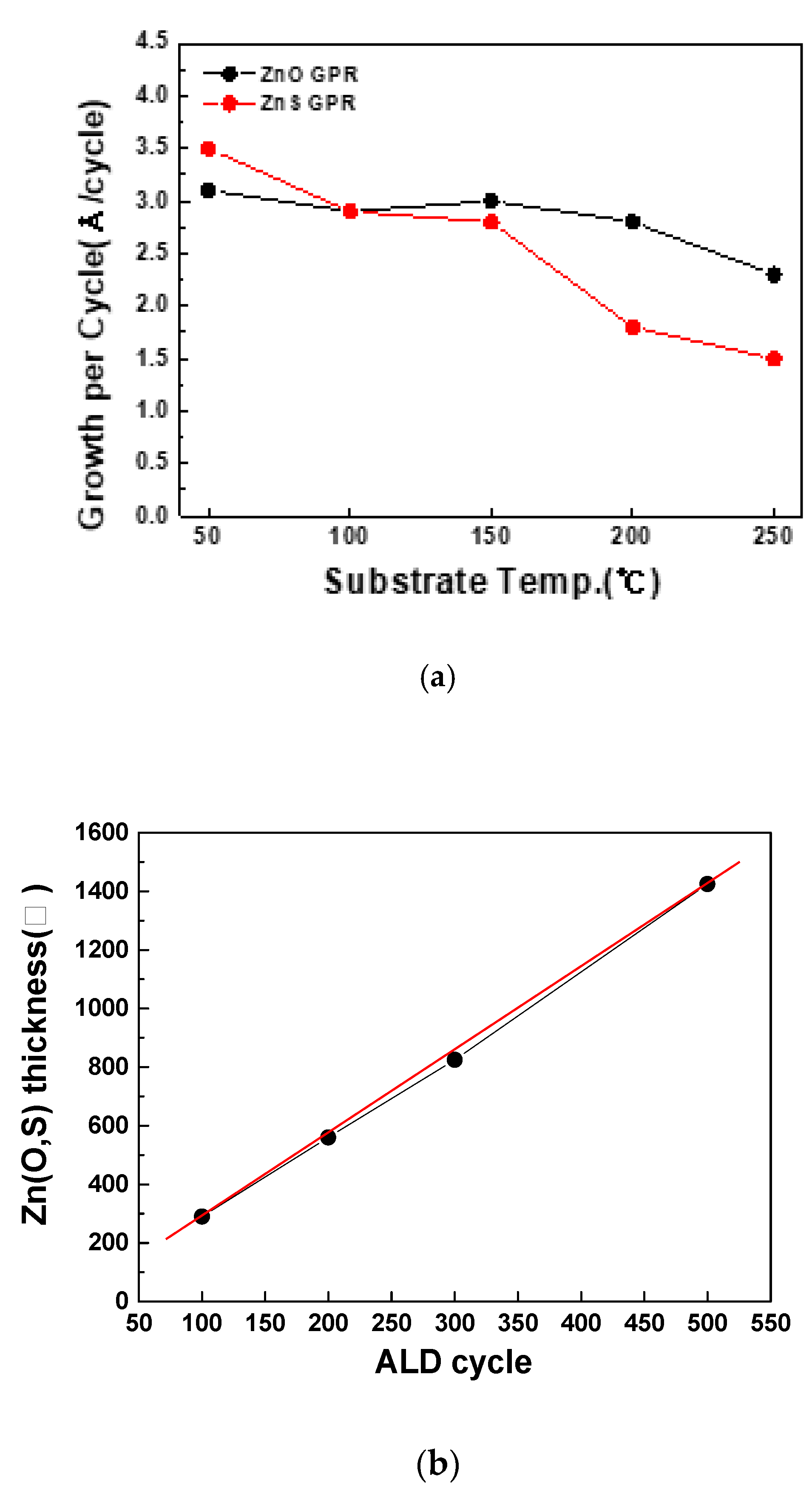
The thickness of the deposited thin films was then analyzed based on SEM images, to verify whether the ALD process had been successfully implemented. In the ALD process, a film is deposited by the self-limiting surface reaction of gas molecules on the substrate surface. Thus, sufficient source exposure time is essential to enable the gas molecules to be uniformly deposited on the substrate as reaction sources. After this sufficient amount of time, the growth rate of thin films starts to saturate. Additionally, at low-temperatures, the deposition rate of thin films remains constant. This temperature window is where the ALD process takes place, i.e., 50–200 °C for ZnO and 90–130 °C for ZnS. These temperatures are highly suitable for process applications because only surface reactions occur in those ranges. As can be seen in
Figure 1, the thin-film thickness linearly increases with the increasing number of ALD cycles, and this implies that the ZnO thin films were successfully deposited on the substrate in the temperature ranges mentioned above [
4,
8,
9].
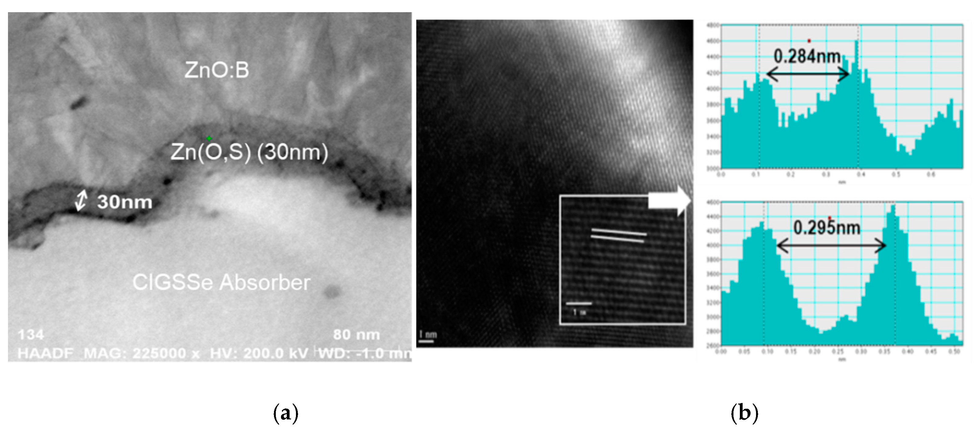
Figure 2 shows the cross-sectional TEM image of Zn(O,S) thin films grown after 100 cycles on CIGS absorber, using ALD at a substrate temperature of 120 °C. The thickness of the TEM sample is approximately 30 nm. In
Figure 2, the good step coverage of the deposited ALD buffer layer can be seen in the cross-section TEM image. The average deposition rate was measured to be 0.29 nm/cycle. From the above observations, we believe that the stable self-limiting growth of Zn(O,S) films was successfully achieved by using ALD at a low substrate temperature of 120 °C [
10].
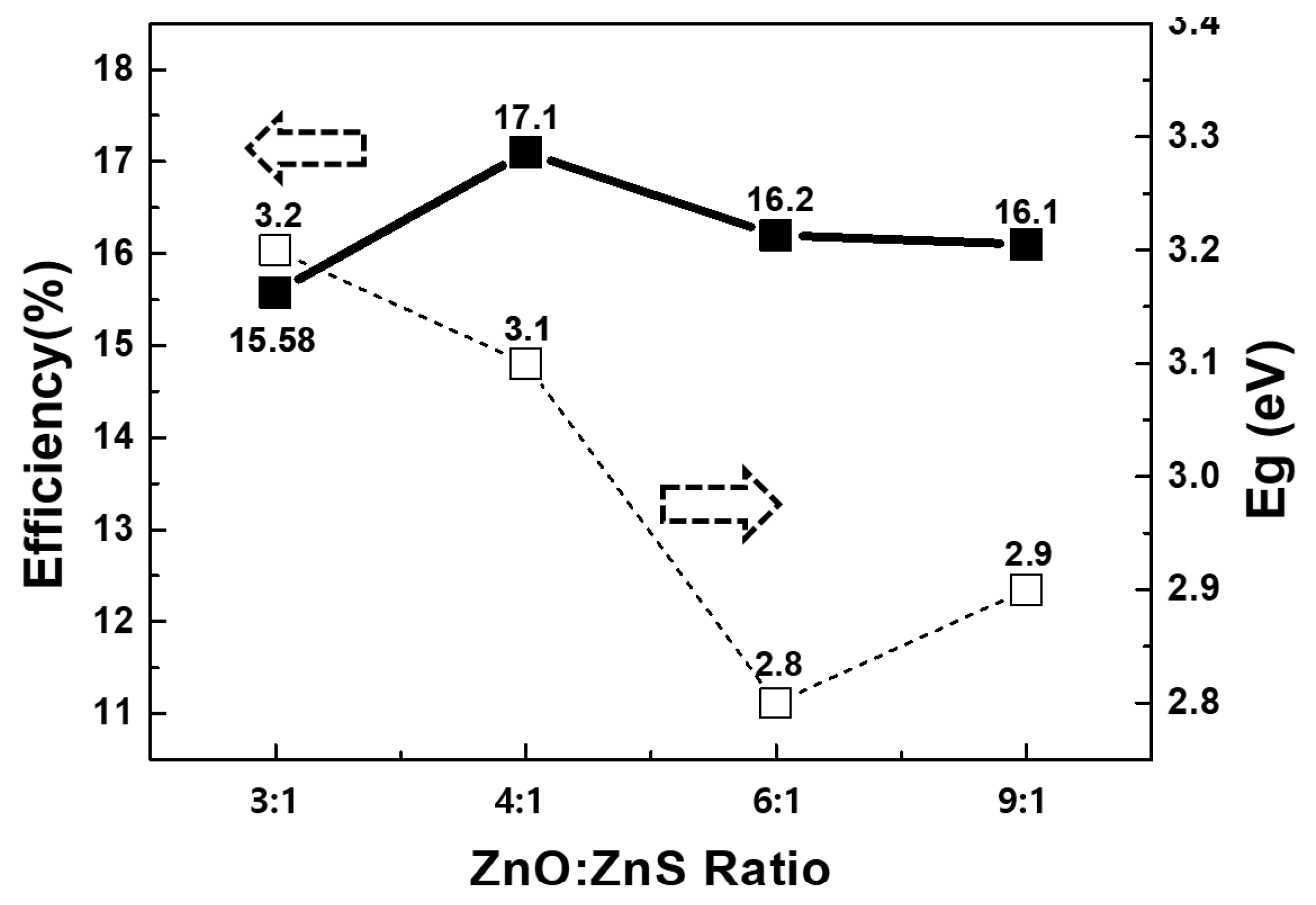
The energy bandgap and photo-conversion efficiency of the CIGSSe solar cells were measured and analyzed with respect to the Zn(O,S) ratio, as shown in
Figure 3. The composition, structure and optical properties of the Zn(O,S) films were determined using samples deposited with 100 cycles on SLG. The total S/Zn ratio in the Zn(O,S) films as a function of the H
2S/DEZn pulse ratio is shown in
Table 1. About S/Zn, we checked sulfur and zinc according to the Zn(O,S) ratio by XPS measuring equipment and also checked the efficiency difference. The sulfur concentration in the films was higher than the fraction of H
2S-containing cycles in the process. For example, the Zn(O,S) 20% process produced a S/Zn ratio of 0.7. One possible explanation for the higher sulfur concentration is that the precursors reacted with the previously deposited film during a pulse. For example, H
2S may adsorb on the surface and consume oxygen in the film by an exchange reaction where water is desorbed as a reaction product. In the case of H
2S/(H
2S+H
2O), it explains the ratio that includes H
2S from all the reactance gas. Additionally, we calculated the bandgap energy after measuring transmittance.
The bandgap energy was analyzed using the optical properties of the deposited Zn(O,S) thin-films. As shown in
Figure 3, the bandgap energy was found to decrease from 3.2 eV to 2.8 eV with decreasing sulfur content in the Zn(O,S) thin-films. The results above demonstrate that it is possible to control the characteristics of Zn(O,S) thin-films by adjusting their composition. Additionally, the results indicate the potential to develop an optimal band structure between the CIGSSe absorber layer and the Zn(O,S) buffer layer using the variation in bandgap energy, depending on the composition [
11,
12,
13].
The application of the ALD method in the deposition of a Zn(O,S) thin-film reduces the occurrence of defects inside the film because the film is formed monolayer by monolayer, and thus, electrons generated by the photovoltaic reaction are less likely to be trapped (or captured) when passing through the buffer layers.
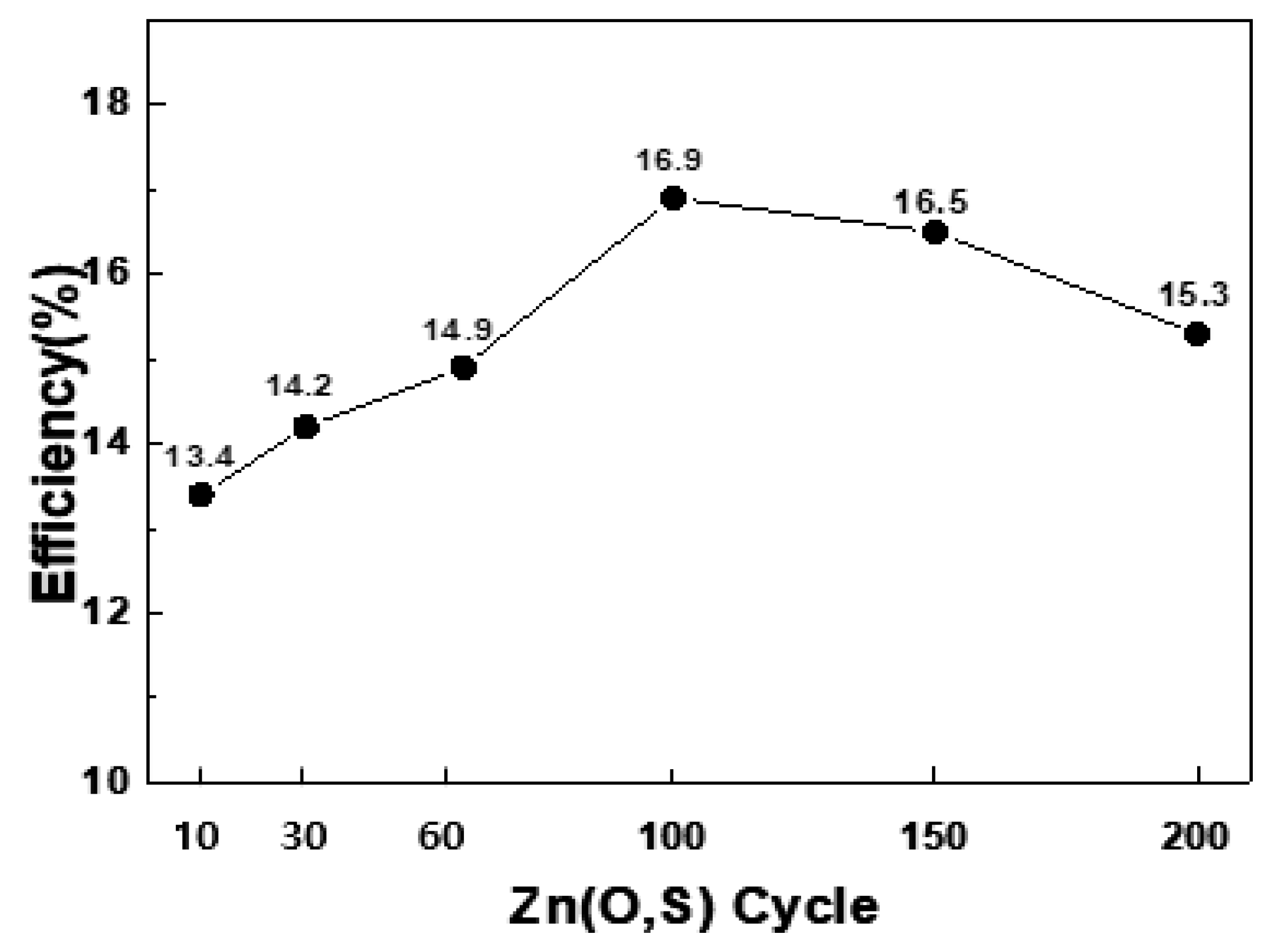
Figure 4 shows how the efficiency of the CIGSSe solar cells changed according to the thickness of the Zn(O,S). When the number of cycles was 100, and the thickness was about 29 nm, the efficiency was determined to be 16.9%, and the efficiency started to gradually decrease, exceeding the thickness threshold. As such, the application of the ALD method for Zn(O,S) deposition makes it possible to precisely control the thin-film thickness by pulse/purge time and vaporization control [
14,
15].
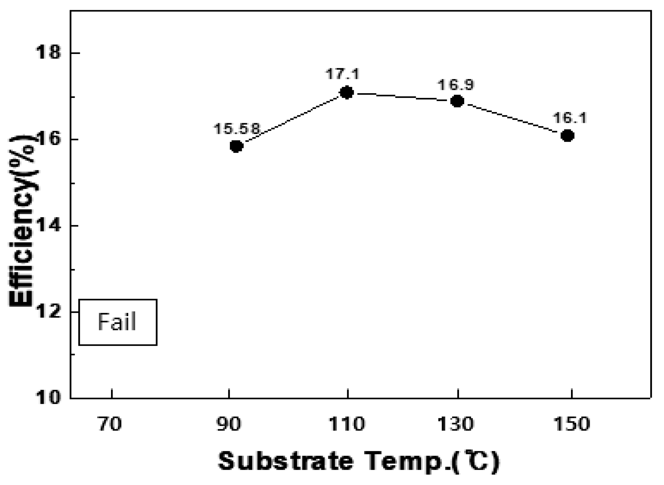
Substrate temperature is one of the very important process parameters of the ALD method when forming ZnO and ZnS thin films. At 110 °C or lower temperatures, the energy is not high enough to cause the reactants to reach each other on the substrate and thus, film growth is slow and it is difficult to achieve the required level of film quality. Additionally, when the temperature is 130 °C or higher for ZnS, and 200 °C or higher for ZnO and DEZn, the precursors are more likely to form multiatomic layers by absorbing substances of the same type, rather than forming monoatomic layers through surface reactions with substances of different types. Another possibility is that H
2S and H
2O precursors may be subjected to pyrolysis, thereby leading to a decrease in the deposition rate [
16,
17].
As mentioned above in
Figure 1, the ALD process is characterized by a specific temperature range called the ALD window. In the present study, it was found that when Zn(O,S) thin films were formed at a constant thin-film deposition rate of 2.9 Å/cycle within the substrate temperature range of 110–130 °C through self-limiting surface reactions, the efficiency was also determined to be at similar levels, e.g., 17.1% and 16.9% as shown in
Figure 5.
4. Conclusions
In the present study, Zn(O,S) thin films were deposited using an atomic layer deposition (ALD) method, and the deposited thin films were examined to investigate their use as buffer layers for high-efficiency CIGSSe solar cells. Additionally, DEZn, H2O, and H2S were used as ALD precursors. It was found that uniform thin films were deposited at a constant deposition rate of 2.9 Å/cycle within the substrate temperature range of 110–130 °C.
The Zn(O,S) layers were deposited by ALD at 120 °C with S/Zn ratios of 0.7 and layers of around 30 nm. The Zn(O,S) 20% (Pulse Ratio: H
2S/H
2O+H
2S) process resulted in a S/Zn ratio of 0.7. As shown in
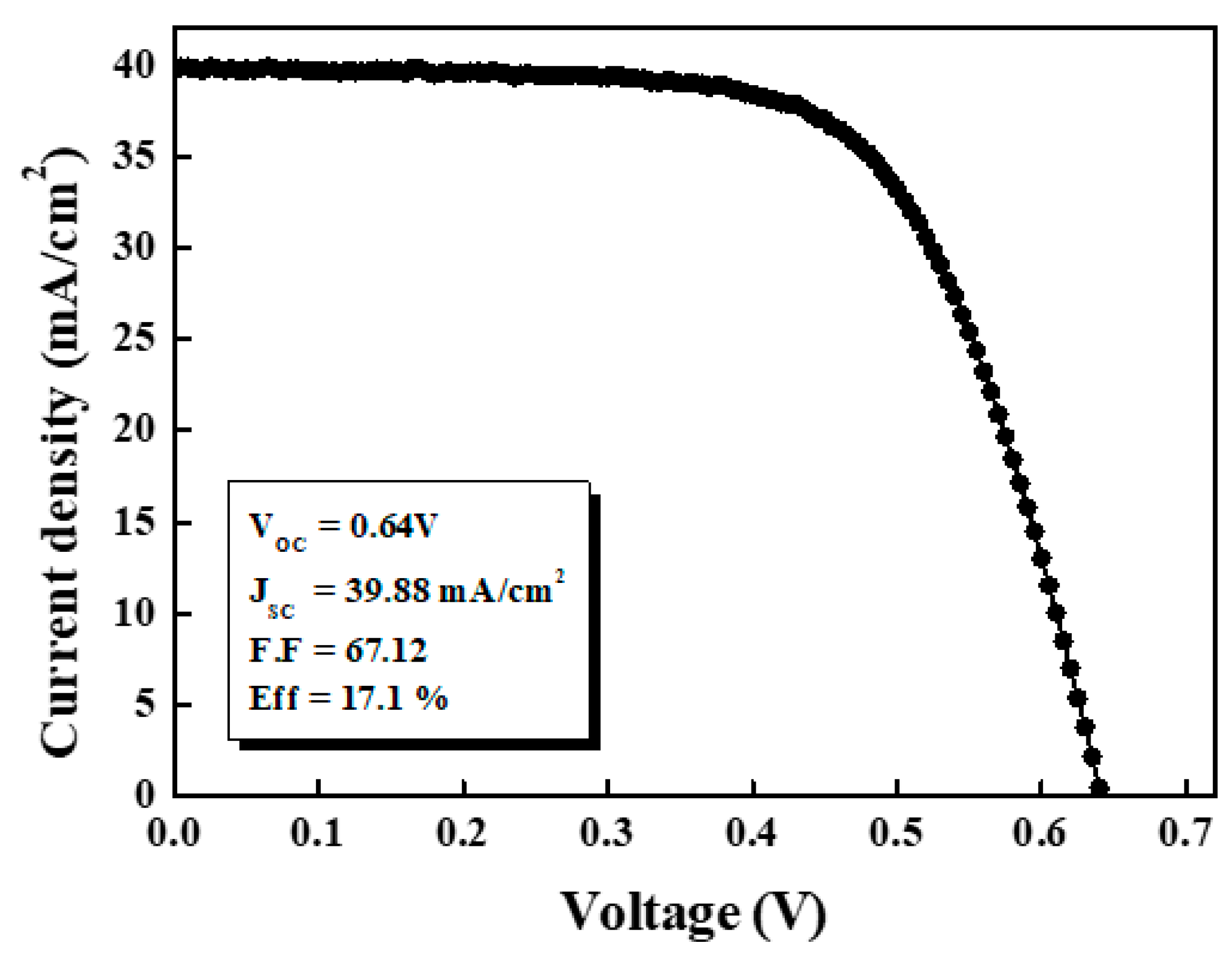
Figure 6, we achieved independently certified aperture area efficiencies of 17.1% for 0.4 cm
2 cells. The open-circuit voltage (V
oc), short-circuit current density (J
sc), and fill factor (FF) were measured to be 0.64 V, 39.88mA/cm
2, and 67.12%, respectively. The thinner than 30nm they are, the values of J
sc and F.F. tend to be reduced. In addition, Zn(O,S) Ratio 3:1, 4:1, 6:1 and 9:1 were all similar V
oc, but we found that the J
sc, F.F. values in those Ratios except Ratio 4:1 were reduced.


