Article

NSGA-II-Based Codesign Optimization for Power Conversion and Controller Stages of Interleaved Boost Converters in Electric Vehicle Drivetrains

1
Department of Electrical Machines and Energy Technology (ETEC) & MOBI Research Group, Vrije Universiteit Brussel (VUB), Pleinlaan 2, 1050 Brussels, Belgium
2
Flanders Make, 3001 Heverlee, Belgium
*
Author to whom correspondence should be addressed.
Energies 2020, 13(19), 5167; https://doi.org/10.3390/en13195167
Submission received: 31 August 2020 / Revised: 27 September 2020 / Accepted: 30 September 2020 / Published: 4 October 2020

Abstract

:
This article proposes a holistic codesign optimization framework (COF) to simultaneously optimize a power conversion stage and a controller stage using a dual-loop control scheme for multiphase SiC-based DC/DC converters. In this study, the power conversion stage adopts a non-isolated interleaved boost converter (IBC). Besides, the dual-loop control scheme uses type-III controllers for both inner- and outer- loops to regulate the output voltage of the IBC and tackle its non-minimum phase issue. Based on the converter architecture, a multi-objective optimization (MOO) problem including four objective functions (OFs) is properly formulated for the COF. To this end, total input current ripple, total weight of inductors and total power losses are selected as three OFs for the power conversion stage whilst one OF called integral of time-weighted absolute error is considered for the controller stage. The OFs are expressed in analytical forms. To solve the MOO problem, the COF utilizes a non-dominated sorted genetic algorithm (NSGA-II) in combination with an automatic decision-making algorithm to obtain the optimal design solution including the number of phases, switching frequency, inductor size, and the control parameters of type-III controllers. Furthermore, compared to the conventional ‘k-factor’ based controller, the optimal controller exhibits better dynamic responses in terms of undershoot/overshoot and settling time for the output voltage under load disturbances. Moreover, a liquid-cooled SiC-based converter is prototyped and its optimal controller is implemented digitally in dSPACE MicroLabBox. Finally, the experimental results with static and dynamic tests are presented to validate the outcomes of the proposed COF.

Graphical Abstract

1. Introduction

In electric vehicle (EV) drivetrains, multiport converters (MPCs) consisting of multiple DC/DC converters have been widely adopted to manage power between different energy sources (i.e., battery, fuel cell (FC) and supercapacitor (SC)) [1]. The DC/DC converters can boost the low voltage range of the energy sources to a high DC-link voltage that feeds to an electric motor (EM) via an electric drive DC/AC inverter [2]. Due to limited space, high reliability and high power-density converters are normally required in EV applications. To this end, wide bandgap technology such as silicon carbide (SiC) MOSFETs have recently been used to replace traditional silicon (Si) IGBTs, which leads to an overall reduction of 30% for the total converter volume [3]. Besides, by applying a multiphase concept along with interleaving operation and current sharing control techniques for the DC/DC converter, its input current ripple, and the sizing of passive components can be remarkably reduced [4]. Beyond that, a holistic and strategic design methodology is needed to unleash the potential of emerging technologies for the power converters.
Traditionally, as shown in the left-side of Figure 1, a sequential workflow comprising three stages has been used to design a DC/DC converter. In the first stage, converter topology is selected and optimized considering the specification of commercial EVs. Each topology selection determines the design constraints for the following steps. Typically, non-isolated (bidirectional) interleaved boost converters (IBCs), have been widely selected as power electronics (PE) interfaces with multiple energy sources [5]. In the second stage, based on a fixed topology, suitable technology and hardware (HW) sizing optimization can be executed separately for components or sub-systems. Finally, in the third stage, the controller or software (SW) is designed considering the constraints created from previous stages. The iterations between stages are conducted until the design requirements are satisfied.
Through the literature, numerous optimization techniques for HW sizing of the PE converters can be classified into four main types: (i) Pareto-front (PF) analysis [6,7,8,9,10] based on brute-force (BF) search (known as exhaustive search), (ii) gradient-based algorithms [11,12,13], (iii) derivative-free based algorithms [14,15,16,17,18,19,20,21], and (iv) other types such as geometry programming [22,23]. Generally, the main design variables involve switching frequency, geometry parameters, inductance- or capacitance- values, and thermal resistance. Those variables are widely selected for different optimization problems (e.g., minimization of sizing, cost, and losses) of various applications such as inductor [14], medium-frequency transformer [18], solid-state transformer [16], AC/DC converter [8], DC/AC converter [24], resonant tank of dual-active bridge [15], power correction factor [13,17], and heat sink [24].
Conventionally, Pareto-front analysis has been used to find an optimal solution from an optimization problem incorporated with multiple design objectives (e.g., volume and efficiency). However, in the Pareto-front method, the optimal solution can be found at the end of an exhaustive search. This searching method sweeps and evaluates all possible combinations of design parameters, resulting in a computationally-intensive process. In contrast, the gradient-based techniques exploit the derivative information of mathematical equations representing objective functions to solve the optimization problem. Nonlinear programming (NP) based on Lagrangian functions [11], augmented Lagrange penalty function (ALPF) [12] and sequential quadratic programming (SQP) [13] can be categorized as the gradient-based techniques. On the other hand, the derivative-free techniques are based on evolutionary nature-inspired algorithms such as particle swarm optimization (PSO) [14,15], differential evolution (DE) combined PSO [16], genetic algorithm (GA) [17] and multi-objective genetic algorithm (MOGA) [18,19,20,21]. A review of those metaheuristic-based optimizations in the PE application was comprehensively reported in [25]. The features of four main techniques for the HW sizing optimization are summarized in Table 1 covering their merits and demerits, main applications, and prevalent objective functions.
Through the extensive literature review, research gaps are identified as follows. It is noticed that the HW and controller designs for the PE converters have been treated independently. So far limited publications have reported possibilities for the coordination architecture of HW-controller codesign. However, especially in the IBC, the potential to combine its HW and controller design in a holistic framework can be feasible for the following reasons. From the HW perspective, an inductance value, which is physically decided by core size and the number of winding turns, should be optimized to minimize the power losses. Besides, from the control aspect, it should be pointed out that in a boost converter, the inductance value has an impact on the position of a right-half-plane (RHP) zero which inherently causes the non-minimum phase issue. The inductance value should be also minimized to keep the RHP zero at high frequency to increase the bandwidth of the closed-loop system, resulting in better dynamic response performance. In this regard, the HW and controller should be codesigned for the IBC. Therefore, this paper focuses on the coordination of HW sizing and SW/controller optimization called a codesign optimization framework (COF) for the IBC in the EV applications, which has been rarely reported in the literature. To this end, the main contributions of this paper may be summarized as follows:
(1)
A simultaneous COF based on metaheuristic-evolutionary searching and automatic decision-making algorithms is introduced for high-power multiphase DC/DC converters in EV applications;
(2)
Four key objective functions involving both the power conversion stage and the controller stage are well-defined in analytical forms to facilitate the optimization process. The optimal results obtained from the COF using those analytical models are verified by finite element analysis (FEA) simulation and experimental results;
(3)
Based on the optimal parameters, a liquid-cooled SiC-based converter and its real-time controller are prototyped and demonstrated. Experimental validations are conducted including (i) a mechanical design for inductor; (ii) integration of the entire converter system in comparison with other prototypes available in the literature; (iii) implementation of field-programmable gate array (FPGA)-based digital controllers; and (iv) static and dynamic load transient testing.
(4)
The proposed COF provides a practical design tool to explore holistically the design space of the PE converter. As the proposed COF is considered as a modular approach, it can be simplified or extended considering other aspects such as reliability and total cost of ownership, which may open new research trends.
As mentioned previously, the MPC contains two separate battery and SC ports with 30 kW/port which employs the same IBC topology, as shown in the right-side of Figure 1. In light of concept verification, the proposed COF and the optimal solution will be mainly demonstrated for the IBC connecting to the battery port (port 1). It should be highlighted that in the entire hardware prototype as demonstrated later on, two ports are shared a common cold plate, yielding a total nominal power of 60 kW.
In this regard, the rest of this paper is organized as follows: Section 2 presents the technology selection for power conversion and controller stages of the IBC. Section 3 explains the formulation of multi-objective codesign optimization problem along with the principle of the proposed simultaneous COF, leading to the optimal solution. Section 4 shows the detailed design of the optimal inductor and its FEA simulation. Section 5 illustrates a full-scale hardware prototype alongside with experimental results. Section 6 presents conclusions and suggests future research trends.

2. Technology Selections of Power Conversion and Controller Stages

This section narrows down the suitable technologies for semiconductor devices and inductors in the power conversion stage along with the control strategy in the controller stage.

2.1. Technology Selections of Power Conversion Stage

The design specifications of the IBC are as follows: nominal power Pnom = 30 kW, output voltage VO = 400 V, nominal input voltage Vin = 200 V, input voltage range from 185 V to 250 V. It is noted that the IBC operates under hard-switching transitions, high power, and high switching frequency. Considering the operating conditions, suitable technologies need to be adopted for the IBC’s critical components. Those components include semiconductor devices and inductors, which mainly contribute to the sizing and performance of the IBC.
Regarding semiconductor devices, wideband gap (WBG) technologies (i.e., silicon carbide (SiC) and gallium nitride (GaN)) have been recently used in for power converters [26]. Among different packages of semiconductor devices, SiC half-bridge (HB) modules are attractive for high-voltage and high-power applications thanks to their modular capability, low packaging loop inductance (about 15 nH to 19 nH), and low thermal impedance [27]. Table A1 in Appendix A shows a comparison between commercially available SiC modules. It is noted that the CAS300M12BM2 (CREE, Durham, NC, USA) and SKM350MB120SCH17 (Semikron, Nuremberg, Germany) share similar packaging. In this study, a commercial 1200 V, 300 A CAS300M12BM2 SiC HB module from Wolfspeed (formerly CREE) [28] is selected for the power circuit because it offers low switching energy, low thermal resistance, and a competitive price.
Regarding the inductor design, the magnetic materials of the inductor core and the winding type are two key factors, which significantly contribute to the weight, volume, power losses of an inductor. Table A2 in Appendix A lists different magnetic core materials used for a multiphase bidirectional converter in EV drivetrains [29] and railway traction [30]. The suitable core material should exhibit high saturation flux, low loss, low cost, and low thermal resistance. Compared to other magnetic counterparts, nanocrystalline materials exhibit many advantages such as favorable high-frequency characteristics up to several hundred kilohertz, high saturation flux density, high permeability and low core loss. However, the manufacturability of nanocrystalline poses high cost and complexity. It can be observed that in automotive powertrains, the amorphous core attracts more interest since it has a suitable temperature, low core losses, and high saturation flux density of 1.5 T [29]. More importantly, the cost of amorphous cores is far cheaper than that of nanocrystalline cores [30]. Regarding the winding selection, compared to the solid-round wire, the Litz-wire conductor has multiple insulated-braided-parallel strands. Hence, Litz-wire can mitigate the AC-winding losses caused by eddy current effects (i.e., skin and proximity effects [31]), improving the inductor efficiency. Another winding type is a copper foil which offers a good utilization of window area, providing increased copper space factor [32]. However, in this paper, multi-strand Litz-wires are more preferable to develop an inductor prototype. To recap, the 1200 V CREE CAS300H12BM2 power modules, iron-based amorphous metal materials (2605SA1 from Hitachi Metglas, a subsidiary of Hitachi Metals America, Ltd, Conway, SC, USA), and multi-strand Litz-wires have been selected for the development of the IBC’s power conversion stage.

2.2. Controller Type and Control Strategy Selections of Controller Stage

In this paper, a dual-loop control architecture consisting of an inner current loop and an outer voltage loop has been selected to regulate the output voltage at a constant set point V O * . Besides, the plant models of duty cycle-to-inductor current G i d ( s ) and duty cycle-to-output voltage G v d ( s ) in the continuous s-domain are required to design the controllers for each loop. To this end, the small-signal averaging technique [4] is employed to obtain the transfer functions of the plants. Table 2 shows the transfer functions of G i d ( s ) and G v d ( s ) which are derived in continuous conduction mode (CCM) [4]. The open-loop gains T i ( s ) and T v ( s ) for the inner current loop and the outer voltage loop can be expressed as Equation (1) and Equation (2), respectively:
T i ( s ) = C i ( s ) G i d ( s )
T v ( s ) = C v ( s ) C i ( s ) G v d ( s ) 1 + T i ( s )
where C i ( s ) and C v ( s ) are the transfer functions of inner current- and outer voltage-controllers, respectively. The plant transfer function G v ( s ) of the voltage control loop is given in Equation (3):
G v ( s ) = C i ( s ) G v d ( s ) 1 + C i ( s ) G i d ( s )
It is noticed that the control-to-output voltage transfer function G v d ( s ) in Equation (5) is a second-order transfer function with one left-half-plane (LHP) zero, one right-half-plane (RHP) zero, and double LHP poles. The effect of RHP zero on the system dynamics can be seen obviously when the duty cycle increases. Initially, the output voltage is reduced, the control command needs to increase the duty cycle of the lower switch. However, the power in the inductor is delivered to the output during the turn-off duration of the bottom switch. Consequently, after 4~5 times of the time constant associated with the RHP zero, the output voltage follows the reference control voltage. To overcome this issue, the loop bandwidth must be selected much less than the frequency of the RHP zero. As can be seen implicitly in (2.6), the inductance L should be minimized to keep the RHP zero ωzv_RHP at high frequency to increase the bandwidth of closed-loop, resulting in better dynamic response performance.
Owning to the occurrence of RHP zero, the IBC suffers a non-minimum phase problem [33]. Due to the problem, it is difficult for a conventional proportional-integral-derivative (PID) controller to perform a desirable performance under dynamic transient load. To overcome the drawback of the traditional PID controller, in this paper, type-III controller is applied for the dual-loop control scheme to achieve a better dynamic response [34]. Generally, a type-III controller is a lead-lead controller with a pole at the origin, which is expressed in Equation (14):
C t y p e I I I ( s ) = K C _ I I I ( s + 2 π f z 1 ) ( s + 2 π f z 2 ) s ( s + 2 π f p 1 ) ( s + 2 π f p 2 )
In Equation (14), K C _ I I I is control gain, f z 1 and f z 2 are frequencies of two zeros (i.e., z 1 = 2 π f z 1 and z 2 = 2 π f z 2 ), respectively, f p 1 and f p 2 are frequencies of two poles (i.e., p 1 = 2 π f p 1 and p 2 = 2 π f p 2 ), respectively. When two zeros, two poles are identical at double frequencies ( f z = f z 1 = f z 2 , and f p = f p 1 = f p 2 ), respectively, Equation (14) becomes Equation (15):
C t y p e I I I ( s ) = K C _ I I I ( s + 2 π f z ) 2 s ( s + 2 π f p ) 2
Conventionally, the double-pole frequency f p and double-zero frequency f z can be determined through the ‘k-factor’ method considering Equation (16) – Equation (19) where ϕ b o o s t ( I I I ) is the phase boost of the controller, f c is the cut-off frequency of controller, | T ( s ) | is the magnitude of open-loop gain determined at the cut-off frequency f c :
K b o o s t ( I I I ) = tan ( 45 o + ϕ b o o s t ( I I I ) 4 )
f z = f c K b o o s t ( I I I )
f p = f c K b o o s t ( I I I )
K C _ I I I = | 1 T ( s ) | f = f c ( I I I )
In the literature, several researchers have adopted PSO [35,36] and the queen-bee genetic algorithm (QBGA) [34] for tuning the control parameters. However, in their research, the controller has been treated independently with the power conversion design. In this paper, the control parameters are simultaneously optimized together with the power conversion design in a holistic codesign framework as explained in the next section. For the sake of performance comparison, the ‘k-factor’ based design is considered as a benchmark to be compared with the optimized design.

3. Proposed Simultaneous Codesign Optimization Framework

Considering the selected structure of power conversion and controller stages as discussed previously, this section presents the development of the proposed COF through four sub-sections. The high-abstract level of the multi-objective optimization (MOO) problem and the definition of codesign variable vector are presented in Section 3.1. Besides, the analytical derivations of objective functions are provided in Section 3.2. The holistic optimization workflow is developed in Section 3.3 to solve the MOO problem, following by the optimal solution in Section 3.4.

3.1. Principle and Flow Chart of Simultaneous Codesign Optimization

Figure 2 shows the block diagram of the power conversion structure coupling with the dual-loop controller architecture and the selected design variables of two stages.
In this research, four objective functions ( O b j F c n ) have been selected for the proposed COF. Regarding the power conversion stage, O b j F c n 1 ( X ) represents the total input ripple current Δ I i n [A], whereas, O b j F c n 2 ( X ) estimates the total weight of inductors W L [kg], and O b j F c n 3 ( X ) determines the total power losses P l o s s [W]. Regarding the controller stage, O b j F c n 4 ( X ) examines the performance of the closed-loop controller through the dynamic response of output voltage by using suitable control criteria. The multi-objective functions are mathematically described as Equation (20):
M u l O b j F n c ( X ) = [ O b j F n c 1 ( X ) O b j F n c 2 ( X ) O b j F n c 3 ( X ) O b j F n c 4 ( X ) ]
where X = [ X P , X C ] denotes the codesign-variable vector consisting of 13 design variables. X P = [ N p h , f s w , i d x c o r e ] is the variable vector of the power conversion stage. Specifically, N p h is a number of phases, f s w is the switching frequency, and i d x c o r e is the core index representing the core geometry parameters extracted from a core database. Besides, X C = [ X C i , X C v ] is the design variable vector of the controller stage. Specifically, X C i = [ z 1 , 2 ( C i ) , p 1 , 2 ( C i ) , K C i ] and X C v = [ z 1 , 2 ( C v ) , p 1 , 2 ( C v ) , K C v ] are the vectors of design variables of the type-III current and voltage controllers that have the transfer functions as in Equation (21) and Equation (22), respectively. In more detail, z 1 , 2 ( C i ) , p 1 , 2 ( C i ) and K C i denotes two zeros, two poles, and the gain coefficient of the current controller C i ( s ) . Similarly, z 1 , 2 ( C v ) , p 1 , 2 ( C v ) and K C v denotes two zeros, two poles, and the gain coefficient of the voltage controller C v ( s ) :
C i ( s ) = K C i ( s + z 1 ( C i ) ) ( s + z 2 ( C i ) ) s ( s + p 1 ( C i ) ) ( s + p 2 ( C i ) )
C v ( s ) = K C v ( s + z 1 ( C v ) ) ( s + z 2 ( C v ) ) s ( s + p 1 ( C v ) ) ( s + p 2 ( C v ) )
The multi-objective optimization problem subjecting to constraints is presented at a highly abstract level in Equation (23) and Equation (24):
min X = [ X P , X C ] Ω X P = [ N p h , f s w , i n d c o r e ] X C = [ X C i , X C v ] { O b j F n c 1 ( X ) = Δ I i n ( X P ) O b j F n c 2 ( X ) = W L ( X P ) O b j F n c 3 ( X ) = P l o s s ( X P ) O b j F n c 4 ( X ) = I T A E ( X P , X C )
s . t . g i ( X ) 0 , i = 1 , m
The optimization constraints gi are listed in Table 3. As Nph and idxcore are integer numbers whereas other variables are continuous, Equation (23) is a mixed-integer optimization problem. Table 4 shows qualitatively the impact of the increases in design variables on objective functions. To cope with the conflicting objective functions, a flow chart using optimization algorithms is proposed to quantify the design variables. In this paper, the multi-objective optimization approach, which relies on mathematical models combined with data of components in the database, is taken into consideration. To simplify the optimization problem, it is assumed that the output capacitor is constant and not involved in the optimization process.

3.2. Objective Functions

This subsection elaborates on the closed-form mathematical models incorporated in the objective functions which are defined in Equation (23).

3.2.1. Objective Function 1: Total Input Current Ripple

The first objective function O b j F n c 1 evaluates the total input current ripple Δ I i n which should be minimized because it has a detrimental impact on the long-term performance degradation of the battery pack connecting to an IBC [37]. Through electrochemical impedance spectroscopy techniques [37], undesired high switching frequency noises and current ripples (i.e., DC-current coupling with AC-current) can increase the capacity face and impedance of battery cells, resulting in differential current flowing into cells and heat generation within the battery pack. If the underlying causality is not properly managed, the battery life will be reduced, degrading vehicle reliability. Hence, it is imperative to minimize the total input current ripple by employing the multiple phases and interleaving technique for the IBC.
The analytical equation of O b j F n c 1 is shown in Equation (25) which is a function of variables N p h , f s w , and L:
O b j F n c 1 = Δ I i n ( X P ) = V O ( D k N p h ) L f s w [ 1 N p h ( D k N p h ) ]
{ 1 V max V O < D < 1 V min V O k [ 0 , N p h 1 ]
where D is the nominal duty cycle. The calculation of inductance value L will be explained in the next objective function.

3.2.2. Objective Function 2: Total Inductor Weights

The second objective function O b j F n c 2 evaluates the total inductor weights W L as given in Equation (27) which is proportional to the number of phases N p h and the weight of a single inductor. An inductor weight mainly composes of a winding weight W w i n d i n g and a core weight W c o r e :
O b j F n c 2 = W L ( X P ) = N p h ( W w i n d i n g + W c o r e )
Traditionally, an inductor can be designed using either K g or A P procedures [38]. In the K g and A P approaches, a core is selected to meet predefined requirements such as limited current ripple and desired inductor losses. In an iteration loop, a checking condition related to the temperature rising in the inductor core is used to evaluate the selected core. If the temperature condition is not satisfied, another core owning a higher value of A P will be re-selected. The K g and A P methods are straight forward. However, they lack the optimality regarding the minimization of inductor losses.
To be distinguished from conventional inductor design, in this paper, the core area product A P represented by the design variable i d x c o r e is decided by the NSGA-II optimization loop to minimize multi-objective functions in Equation (23). In this paper, a database of different amorphous cores is prepared. Each inductor core is labeled by an integer number i d x c o r e including main core parameters (the window area W a [mm2], the net cross-sectional area A C [mm2], the core area product A P = W a A C [mm4], the saturation flux density B max [T], the core window utilization factor K u , and the core weight W c o r e [kg]). Once a specific i d x c o r e is picked up by the NSGA-II, its characterized parameters are fetched and cast into Equation (28) (see Appendix C) to obtain an attainable inductance value L [µH]. It is noted that the inductance value should be a real root of the second-order polynomial equation (28):
L 2 I L ( c r i t ) 2 + L [ I L ( c r i t ) ( 1 D max ) D max f s w K u J w i r e B max ( W a A C ) ] + [ V O ( 1 D max ) D max 2 f s w ] 2 = 0
As can be seen in Equation (28), the inductance value is determined under the critical condition of boost operation. The critical condition occurs when the input voltage reduces to the minimum voltage V i n ( min ) . As a consequence, the duty cycle increases to a maximum value D max to maintain a fixed output voltage V O . Furthermore, in the critical condition, the core (with a saturation flux density B max ) needs to be not saturated when the inductor current reaches the peak value I L ( c r i t , p k ) = I L ( c r i t ) + 1 2 V O ( 1 D max ) D max f s w L . In the critical condition, the average inductor current is given as I L ( c r i t ) = P max N p h V O ( 1 D max ) .
Based on the inductance value, the number of turns N t u r n and air-gap length l g a p are calculated as Equation (29) and Equation (30), respectively. The air-gap length l g a p [mm] is added to prevent the core saturation:
N t u r n = r o u n d ( L I L ( c r i t , p k ) A C B max )
l g a p = N t u r n μ 0 I L ( c r i t , p k ) B max
where μ 0 = 4π.10−7 [H/m] is the vacuum magnetic permeability. Based on the number of turns and core geometries, once the winding length is estimated, the winding weight W w i n d i n g can be calculated considering the winding weight density [kg/m] of the Litz wire. Therefore, the O b j F n c 2 in Equation (27) can be completely determined.

3.2.3. Objective Function 3: Total Converter Losses

The third objective function O b j F n c 3 evaluates the total converter losses P l o s s . Accordingly, optimization-oriented and analytical equations representing the governing losses of components (i.e., SiC HB modules and inductors) with their nonlinearities are developed to estimate the power loss distribution. The total converter losses are mainly governed by the MOSFET losses P l o s s ( M O S F E T ) , the diode losses P l o s s ( D I O D E ) , and the inductor losses P l o s s ( L ) as shown in Equation (31):
O b j F n c 3 = P l o s s ( X P ) = N p h ( P l o s s ( M O S F E T ) + P l o s s ( D I O D E ) + P l o s s ( L ) )

Semiconductor Losses

As this paper focuses on high power converter applications, only critical and major losses will be considered for the loss model of semiconductors. It is noted that MOSFET and diodes are operated as switches, taking on various static and dynamic states in cycles. Individual power losses of switches can be broken down into static losses (i.e., on-state/conduction loss and blocking loss), switching losses (i.e., turn-on loss, turn-off loss, output parasitic capacitor loss, and gate driver loss). The accurate losses model of SiC power modules can be found in [39]. However, in this paper, several simplifications for the converter loss calculation can be conducted to facilitate the optimization process as follows:
(i)
Dead-times loss is neglected,
(ii)
The output capacitor loss owning to its equivalent series resistance (ESR) is neglected,
(iii)
Junction temperatures are in time constant at 150 °C for the sake of conservative calculation, and the converter operates at the nominal rating power,
(iv)
Gate driver loss are neglected because they are considered only for low-power, low-voltage MOSFET applications with very high frequency,
(v)
Loss owning to discharging parasitic output capacitor, forward-blocking losses can be neglected in the high-power applications since they only account for a small share of the total power dissipation [40]. In case of high blocking voltages (>1000 V) and/or high operating temperatures (>150 °C), blocking losses may gain importance and may even result in thermal runaway owing to the exponentially rising reverse currents.
The MOSFET losses in Equation (32) can be broken down into the conduction loss P c o n d ( M O S ) and switching losses P s w ( M O S ) (i.e., turn-on and turn-off losses). Similarly, the diode losses in Equation (33) can be broken down into the conduction loss and reverse recovery losses:
P l o s s ( M O S F E T ) = P c o n d ( M O S ) + P s w ( M O S ) = R D S ( o n ) I D S ( r m s ) 2 + V O V D S ( r e f ) I D S ( r m s ) I D S ( r e f ) f s w ( E o n ( @ I D S ( o n ) ) + E o f f ( @ I D S ( o f f ) ) )
P l o s s ( D I O D E ) = R F I D ( r m s ) 2 + V O V D S ( r e f ) I D ( r m s ) I F ( r e f ) f s w [ E r r ( @ I D ( a v g ) ) ]
From the manufacturer’s datasheet, the characteristics of the SiC HB module are stored in look-up tables to interpolate the switching losses in different operating currents. Figure 3 shows the switching energy dissipations (i.e., E o n , E o f f ) of MOSFET and the reverse recovery energy loss (Err) of the diode, which are measured under the double-pulse test for given DC-bus voltage V D S ( r e f ) and drain-to-source current I D S ( r e f ) at 25 °C and 150 °C. In this regard, the estimated losses of MOSFET and diode can be scaled up or down according to the variations of design variables during the optimization process. Moreover, the currents I D S ( o n ) , I D S ( o f f ) , I D S ( r m s ) , I D ( r m s ) , I D ( a v g ) need to be determined to find the energy losses in Equation (32) and Equation (33).
Table 5 shows the calculations of those currents for the MOSFET and the diode. It is noted that in the boost operation, the bottom MOSFET of a phase leg conducts the inductor current during its on-period and the anti-parallel diode of the top MOSFET takes over the inductor current during the off-time of bottom MOSFET.

Inductor Losses

The inductor losses P l o s s ( L ) mainly consist of winding losses P w i n d i n g ( L ) as in Equation (40), core losses P c o r e ( L ) as in Equation (44), and air-gap losses P g a p ( L ) as in Equation (46). The winding losses P w i n d i n g ( L ) can be further classified as AC-winding loss P a c ( L ) and DC-winding loss P d c ( L ) . The DC-winding loss as in Equation (41), known as a resistive loss, can be estimated by a DC-resistance R d c ( L ) and RMS current I L ( r m s ) flowing through the designated inductor. The DC-resistance R d c ( L ) as in Equation (43) can be determined by copper resistivity ρ r e s ( c o p p e r ) = 16.78 × 10⁻⁹ [Ω.m], total winding length l w i n d i n g , and conductor cross-sectional area A w i r e . The AC-winding losses P a c ( L ) from the skin depth effect and the proximity effect can be neglected ( P a c ( L ) = 0) because the Litz-wire is utilized:
P w i n d i n g ( L ) = P d c ( L ) + P a c ( L )
P d c ( L ) = R d c ( L ) I L ( r m s ) 2
I L ( r m s ) = I L 2 + ( Δ I L ) 2 12
R d c ( L ) = ρ r e s ( c o p p e r ) l w i n d i n g A w i r e
The core losses Pcore(L) are estimated in Equation (44). This equation is a modified version of the Steinmetz equation with a correction factor for the non-sinusoidal excitation in which the unidirectional flux density ripple Bac [T] is proportional to the inductor current ripple ΔIL where W c o r e [kg] is the weight of the core, coefficients K c o r e = 6.5, α f = 1.51, β B = 1.74 are given in the manufacturer datasheet [41], Δ I L is the inductor current ripple, and l g a p [cm] is the length of the air-gap:
P c o r e ( L ) = W c o r e ( K c o r e f s w α f B a c β B )
B a c = 0.4 π N t Δ I L 10 4 l g a p
The prediction of air-gap loss Pgap(L) expressed in Equation (46) is a power function [42] of the total gap length lgap, core lamination width Dcore, frequency fsw, and given peak AC-flux density Bac(peak), where k g , k l g , k D , k f , k B a c are numerical coefficients provided by the core manufacturer. In this paper, as the inductor core has a high permeability based on its finely laminated structure, the fringing effect is relatively small at air-gap, which can be neglected:
P g a p ( L ) = k g l g a p k l g D c o r e k D f k f B a c ( p e a k ) k B a c

3.2.4. Objective Function 4: Integral of Time-weighted Absolute Error for Output Voltage Control

In the EV drivetrain, the main purpose of the IBC is to maintain a fixed DC-link voltage regardless of battery voltage variation and output load disturbances. In this regard, the fourth objective function O b j F n c 4 evaluates the performance of output voltage control via the dynamic response of closed-loop. The objective of the controller is to minimize the dynamic error signal e ( t ) during the transient time when the load changes. Some control criterion can be considered for the O b j F n c 4 as following: integral of squared error ( I S E = 0 τ e 2 ( t ) d t ), integral of absolute error ( I A E = 0 τ | e ( t ) | d t ), integral of time-weighted absolute error ( I T A E = 0 τ t | e ( t ) | d t ), integral of time-weighted squared error ( I T S E = 0 τ t e 2 ( t ) d t ), integral of the time-squared weighted squared error ( I T 2 S E = 0 τ t 2 e 2 ( t ) d t ), and integral of the time-squared weighted absolute error ( I T 2 A E = 0 τ t 2 | e ( t ) | d t ). An upper limit τ is chosen as a steady-state value.
As can be seen, the ISE and IAE treat the error signal e ( t ) equally at any time instance. In contrast, the ITAE penalizes the error signal e ( t ) along with a long duration transient, that leads to the error signal being forced to reduce to zero as soon as possible. Moreover, the ITAE generally produces less overshoots and oscillations compared to other criterion [33]. Therefore, in this paper, the ITAE is selected to evaluate the controller performance. The ITAE of the output voltage is mathematically expressed in Equation (47):
O b j F n c 4 = I T A E V O ( X P , X C ) = 0 τ t | e V O ( t ) | d t
As recognized previously, the inductance value L influences the RHP zero and the bandwidth of the closed-loop system. Physically, L is also dependent on the i d x c o r e which is a design variable in the vector X P . Therefore, O b j F n c 4 is a function of both X P and X C . In the control design process, the O b j F n c 4 is evaluated from the step response of the voltage controller C v ( s ) considering the plant transfer function G v ( s ) in Equation (3).

3.3. Principle of Simultaneous Codesign Optimization

Four considered objective functions have been derived in analytical equations that are implicitly composed of design variables. This section explains how to incorporate the optimization algorithms to solve those objective functions, creating a holistic COF.
Figure 4 elaborates on the flow chart of the proposed COF. In this research, the NSGA-II [43] and average ranking (AR) [44] are combined to solve the mix-integer, highly nonlinear, and non-convex multi-objective optimization problem in Equation (23) under the list of constraints given in Equation (24). The NSGA-II was developed by Deb et al. [43]. In NSGA-II, the genetic algorithm (GA) plays as a searching kernel with two new additional functions to achieve better multi-objective optimization. These two added concepts are ‘fast nondominated sorting’ and ‘crowding distance assignment’. NSGA-II uses a Pareto-front hierarchy and adopts an elitism mechanism to retain the best solutions generated during the search. By using the discrete value of design variable i d x c o r e , the optimization process fetches individual parameters in the core database to calculate each objective function.
The NSGA-II algorithm starts by initializing the parent population randomly. Each of the four objective values is evaluated accordingly. The population is made up of 50 individuals (population size) that are characterized by a vector consisting of a codesign variable X = [ X P , X C ] , objective values { O b j F n c 1 ; ... ; O b j F n c 4 } , overall fitness value, and neighborhood diversity value. For each generation, the individuals from parent and offspring populations are classified on several fronts by considering the non-dominance. It is called ‘fast nondominated sorting’ which uses a ranking concept to assign a fitness value to each solution, facilitating the selection process in the GA. The first front contains all non-dominated solutions (rank 1). The second front sorts the solutions (rank 2) dominated by only one solution. The third front has solutions (rank 3) dominated by two other solutions. This process continues until no solution is left. To maintain the diversity of solutions in case of the same front, the additional sort called ‘crowding distance assignment’ is performed. The crowding distance algorithm calculates how far away the neighbors of a given solution are. In the next step, an ‘elitism selection operator’ uses a binary tournament to select individuals of the lower front (or lower rank) and the solution with greater crowding distance in case of the same front. New populations are generated by ‘genetic operations’ such as simulated binary crossover and polynomial mutation.
The NSGA-II is terminated when the maximum generation of 200 is reached. A set of design solutions found is returned as the Pareto-front in which no other solutions are superior to those in its set when all objectives are considered. In other words, in the Pareto-front, each candidate solution can be considered equally good. A common post-processing approach is that the designer with their preference and design experience could select a compromised solution from amongst Pareto front solutions. This approach is dependent on the designer’s decision, which may fail to find a truly optimum. Therefore, in this paper, the AR [44] as a decision-making step is added to pick up an optimal solution from the Pareto-front.
Basically, the AR calculates a score for each candidate solution s i by summing the ranks of s i for each objective function. If s i , for example, is the first, second, third, and fourth best on the O b j F n c 1 , O b j F n c 2 , O b j F n c 3 , O b j F n c 4 , respectively, the AR score of s i will be 1 + 2 + 3 + 4 = 10. The s i having the lowest score is chosen for the optimal solution.

3.4. Optimal Solution

As shown in Figure 5, the optimal solution at the low right corner of its data tip popup is highlighted in the 3-dimension (3D) Pareto-front. The total inductor weight ( O b j F n c 2 ) is 2.4 kg, the input current ripple ( O b j F n c 1 ) is 3.6 A, and the converter losses ( O b j F n c 3 ) are 440 W meaning that the converter can theoretically achieve an efficiency of 98.5% at 30 kW. The optimal design solutions for the power conversion stage and the controller stage are summarized in Table 6.
To verify the performance of optimized control, an IBC model for time-domain simulation is developed in the Matlab Simulink using SimPowerSystems. The output voltage is regulated at a fixed voltage of 400 V. At t = 0.05 s, the output load current modeled as a current source increases from 75 A to 150 A and decreases from 150 A to 75 A at t = 0.1 s. The type-III current- and voltage-controllers based on the ‘k-factor’ approach are designed as a benchmark.
Figure 6 shows the simulation responses of output voltage, input current, and inductor current when the load current changes. The optimized type-III controllers exhibit faster dynamics in both current and voltage loop in comparison with the ‘k-factor’ based controllers, resulting in reductions in undershoot (−25%) and overshoot (−45%) for the output voltage. Compared to the ‘k-factor’ approach, the settling time for the optimized controller can be reduced from 25 ms to 10 ms.

4. Inductor Design

This section presents detailed inductor design using the optimal parameters obtained from the previous sections. Computer-aid-design (CAD) and FEA tools are used to verify the inductance value and its temperature rise, which supports to avoid the trial-and-error iteration in the practical design.
Figure 7a,b show FEA results attained from ANSYS Maxwell for the inductor using the optimal parameters in Table 6. It is noted that the inductor simulation uses a lumped copper foil model because it is impractical to draw a model of Litz-wire. Besides, the modeling of individual laminations (18 µm thickness) inside the core is not considered feasible. Hence, the inductor core can be modeled by a solid continuum. However, the FEA inductor model can preserve the anisotropic properties of the laminated structure utilizing a homogenized approach [42].
In the ANSYS Maxwell, the mesh size is 3mm and the excitation current flowing through the winding is a triangular DC-biased current (55 A average DC-current and 3.8 A current ripple). As can be seen in Figure 7a, the maximum flux density of 1.4 T is obtained at the corners of the window area, whereas the average flux density is about 1T through the mean path length of the inductor core. The flux density values are lower than the saturation flux (1.56 T) of the selected amorphous core. As can be seen in Figure 7b, the average inductance value of 175 µH is achieved with 17 turns and 1.6 mm air-gap.
Figure 8 illustrates the FEA thermal distribution of an inductor. The inductor winding which generates power losses of 6 W is selected as a heat source. Due to free convective heat transfer, the temperature rise on the surface of the inductor core is predicted about 68 °C.
An inductor prototype is demonstrated in Figure 9a while the core dimension is shown in Figure 9b. Inductor prototypes are designed using the amorphous core AMCC50 from Metglas, rectangular Litz-wire from Von Roll Isola (Belfort, France, 0.2 kg/m, 2600 strands, the strand diameter is 0.1 mm, and RMS rating current is 60 A), and nylon bobbin. The three materials allow operating temperatures higher than 200 °C. The weight of an inductor is 1 kg due to additional screws and metal strip fastener. As the air gap lengths and winding lengths of inductors are not identical, the measured inductance of three phases are 175.7 µH, 173.5 µH, and 175.4 µH, respectively, which are slightly deviated from the desired value 175 µH. The unbalanced inductor currents due to the inductance deviation can be compensated by the closed-loop controllers.

5. Prototype Demonstration and Experimental Results

This section depicts a full-scale converter prototype in comparison with other published prototypes available in the literature. Besides, this section presents the FPGA implementation of digital controller before showing the verified experimental results.

5.1. Proposed Hardware Prototype and Comparison

As mentioned in the introduction, the MPC consists of two separate ports (30 kW/port) that can employ the same IBC topology for the sake of simplicity and modularity. It is noted that the proposed COF has been demonstrated above only for the IBC connecting to the battery port. Similarly, the proposed codesign methodology can be applied for the IBC of the SC port with the input voltage range of 200 V~400 V. The optimal inductance for the SC port is 145 µH which can be realized by using the same AMCC50 core and Litz wire as described in Figure 9b, except for a 15 turns winding. In this regard, a 60 kW MPC prototype has been fabricated to demonstrate the feasibility of the proposed COF.
Figure 10a shows the CAD model of a custom-made cold plate using liquid-cooling to ensure the peak junction temperature of the SiC MOSFET modules in the safe operation. Figure 10b depicts the actual implementation of SiC HB modules mounting on the top side of the cold plate. Laminated busbar which comprises two parallel aluminum plates separated by dielectric materials are designed to reduce the stray parasitic inductance of the DC-link. A heat exchanger with a pump is connected to the cold plate to circulate the coolant with the volumetric fluid flow rate of 4 L/min.
Figure 11a,b show the overview and side-view layout of functional subsystems. Six SiC HB modules are mounted on the top of the cold plate, whereas six inductors are attached to its bottom side. In case, by leveraging the automated reconfigurable concept with the aid of controlled relays, the two ports based on two three-phase IBCs can be converted to a single six-phase IBC, increasing power capability. This approach enhances the scalability and modularity for the entire converter system, reducing the total cost of ownership.
Table 7 compares the system specifications between the proposed prototype and different multiphase DC/DC prototypes including a battery charger [45], a railway traction converter [3], and a multidevice interleaved boost converter (MDIBC) [4] which are available in the literature. The published converters with amorphous cores are selected for the sake of a fair comparison. Several comments can be made as follows. First, it should be highlighted that by increasing switching frequency, inductor size can be reduced for the proposed SiC-based converter, resulting in overall reductions in weight and volume by 40% and 35%, respectively, compared to the Si-based IGBT MDIBC.
Second, as the discrete TO-247 packages offer lighter weights compared to the 62 mm HB packaging, the discrete-based design in [45] has a gravimetric power density higher than the proposed prototype. However, in the converter using discrete TO-247 packages, some challenges for gate driver design should be taken into account to avoid unbalanced currents and cross-talk between parallelized MOSFETs. The main purpose of this paper is to demonstrate the feasibility of the codesign methodology involving both hardware and controller optimization. There is still room for the optimization of component arrangement and thermal management to achieve higher power density, which is considered as our future work.

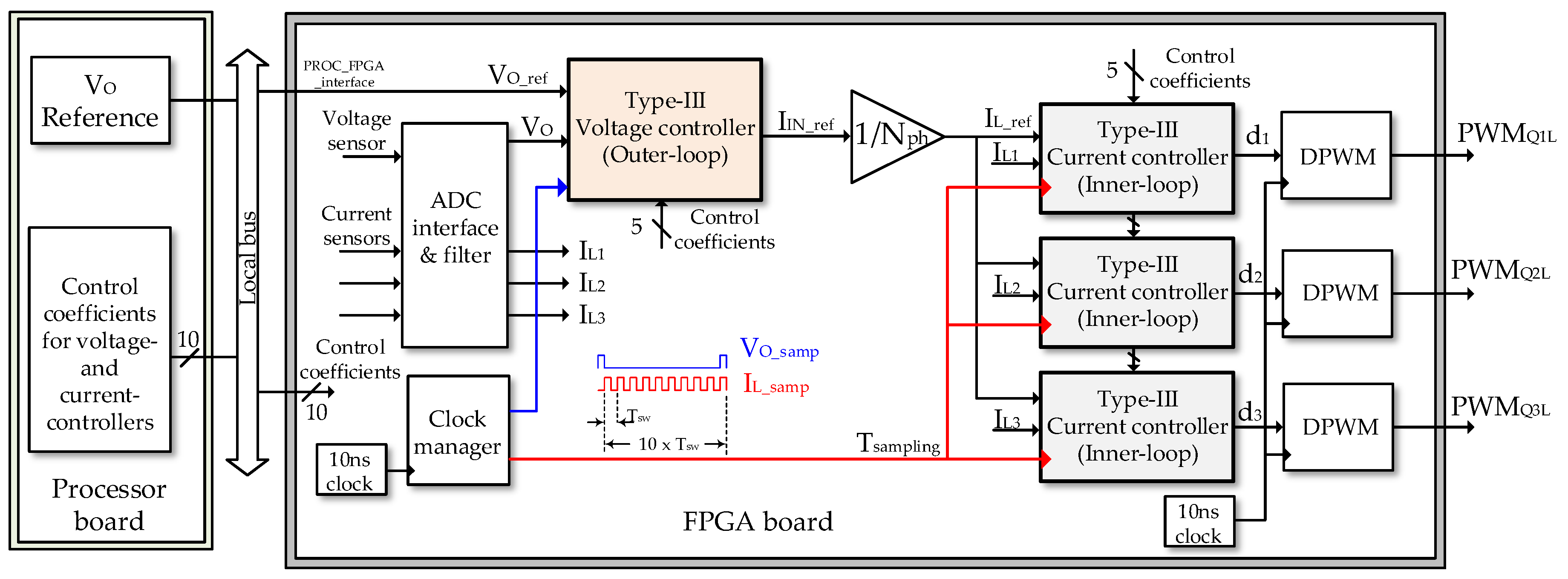
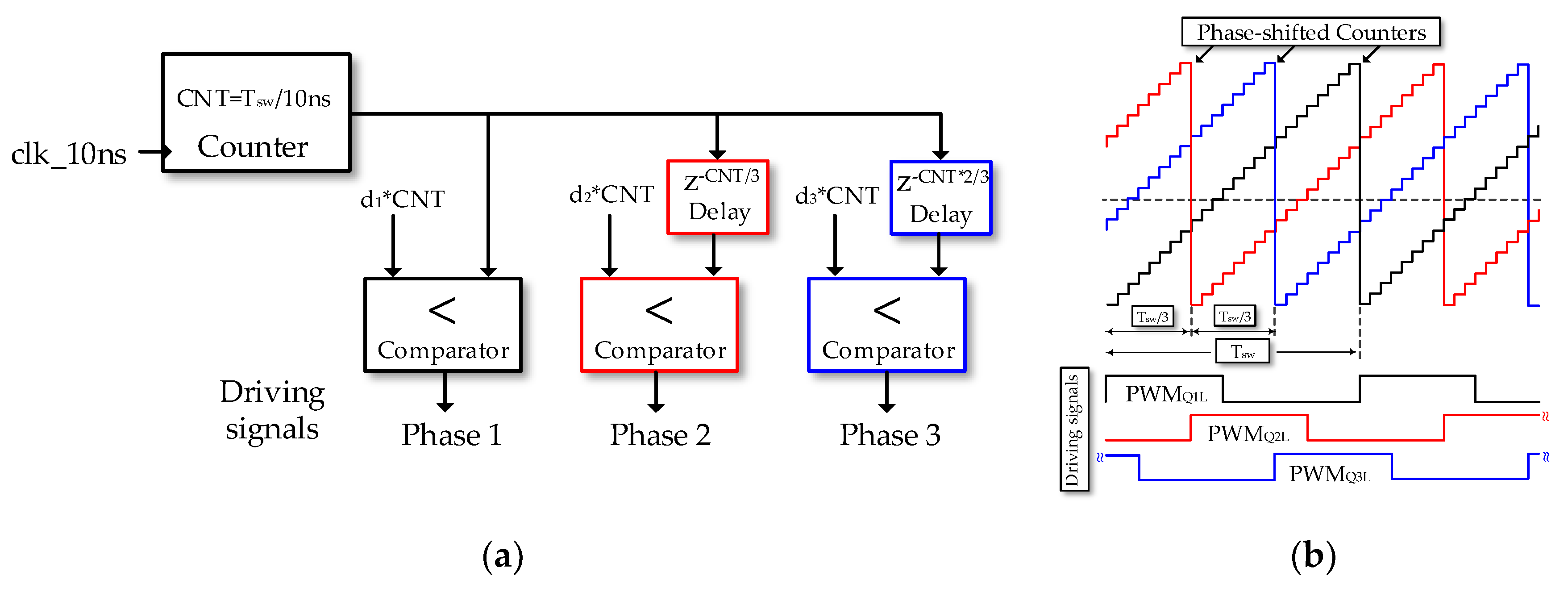
5.2. FPGA Digital Control Implementation

In this paper, the digital controller is implemented based on a digital redesign approach. Once the transfer functions of the controllers C i ( s ) and C v ( s ) are obtained in the s-domain, they are discretized using the Tustin transformation ( s 2 T s a m p l i n g z 1 z + 1 ). The Tustin transformation provides a good agreement in the frequency domain between the continuous- and discrete- transfer functions [46]. Typically, a good choice for the discretized sampling period T s a m p l i n g is equal to the switching period T s w ( = 1 / f s w ). Besides, in practice, the sampling period of the controller and the sampling period of analog-digital-converter (ADC) are the same. The sampling instants of the ADC are carefully selected when the bottom switch turns off to minimize errors induced by the switching noise.
In this paper, the standard form-I is adopted to implement the difference equation of the discrete transfer function thanks to its simplicity, configurability, and scalability [46]. Moreover, debugging is convenient as the error signal and the output reference signal can be followed independently in the difference equation. The discrete controller C ( z ) in Equation (48) can be translated into the difference equation through the inverse z-transform as Equation (49) so that it can be implemented via a direct form-I:
C ( s ) s = 2 T s a m p l i n g z 1 z + 1 C ( z ) = u ( z ) e ( z ) = i = 0 3 a i z 3 i i = 0 3 b i z 3 i = i = 0 3 a i z i i = 0 3 b i z i
u k = 1 b 0 ( a 0 e k + a 1 e k 1 + a 2 e k 2 + a 3 e k 3 b 1 u k 1 b 2 u k 2 b 3 u k 3 )
In Equation (48), u ( z ) is the output control signal, e ( z ) is the error between the reference signal and the measured signal. Where e k , e k 1 , e k 2 , e k 3 is the present, one-sample period, two-sample period, three-sample period delayed values of the error signals, respectively. Similarly, u k , u k 1 , u k 2 , u k 3 is the present, one-sample period, two-sample period, three-sample period delayed values of the output control signals, respectively. In the outer loop, the output voltage controller C v ( z ) generates u ( z ) as the reference control signal of total inductor currents I r e f for the inner loop in which the current controller C i ( s ) generates the required duty cycle.
The discrete transfer functions in the z-domain of current- and voltage- digital controllers based on the optimized design and the ‘k-factor’ design are expressed in Equation (50)– Equation (53), respectively:
C i ( o p t ) ( z ) = 0.044 z 1 0.064 z 2 + 0.0231 z 3 1 1.6074 z 1 + 0.6917 z 2 0.0843 z 3
C v ( o p t ) ( z ) = 0.1985 z 1 0.3875 z 2 + 0.1891 z 3 1 2.8020 z 1 + 2.6137 z 2 0.8117 z 3
C i ( k f a c ) ( z ) = 0.0168 z 1 0.0273 z 2 + 0.011 z 3 1 1.475 z 1 + 0.5308 z 2 0.0563 z 3
C v ( k f a c ) ( z ) = 0.1348 z 1 0.2646 z 2 + 0.1298 z 3 1 2.732 z 1 + 2.482 z 2 0.75 z 3
Figure 12 shows a simplified block diagram of the digital control system. The control platform used in this paper is dSPACE MicroLabBox which includes two main boards (i.e., processor board DS1202 and FPGA board DS1302). The voltage reference setpoint and control coefficients can be set from the processor part which communicates with the FPGA board via local buses. The dual-loop control scheme is implemented on the FPGA board. The form-I digital implementation for type-III controller based on Equation (49) is realized using Xilinx System Generator (XSG) blocksets such as adder, multiplier, registers. Additional configuration steps of the FPGA are needed to convert the XSG block program into the VHDL code. To this end, a VIVADO software version 17.2 provides an automatic synthesis and place-and-route tool to ultimately generate the bitstream file. The file can be downloaded into Xilinx Kintex-7 XC7K325T FPGA (10 ns period clock) embedded in the DS1302 board.
Figure 13a shows the principle of digital pulse width modulation (DPWM). A 16-bit count-limited counter is used to create a sawtooth carrier of the DPWM. As shown in Figure 13b, the period of the PWM is measured from zero to the limited counting value in the counter cycle. The phase-shift between each phase is realized by delay blocks.

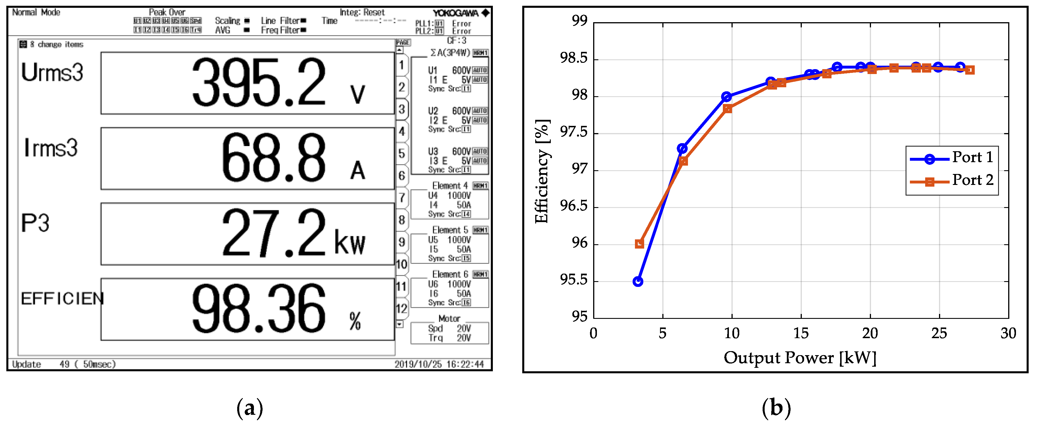
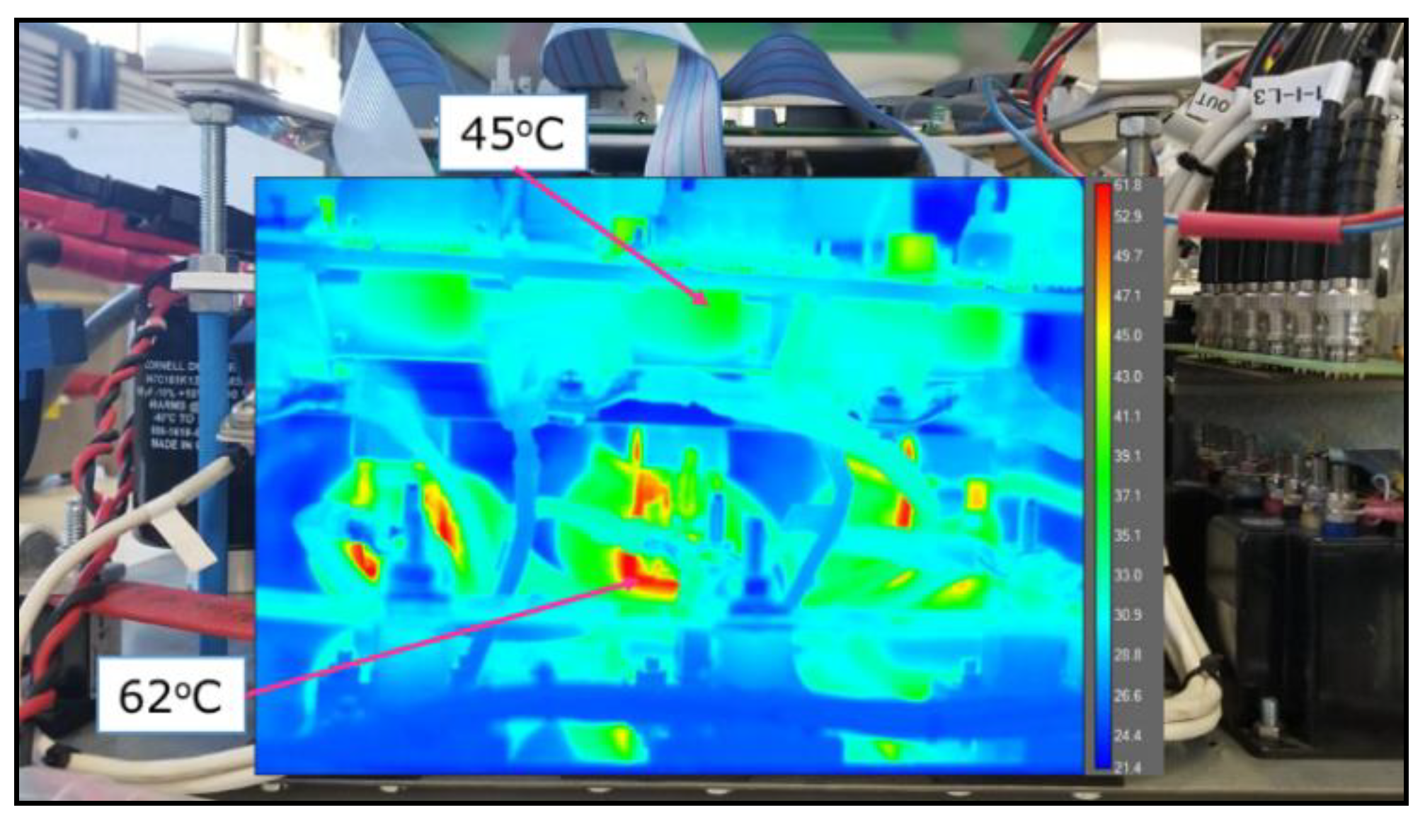
5.3. Experimental Results

An experimental test bench was prepared in our laboratory. During the test procedure, a fixed input voltage is provided from a DC power supply. The output voltage is regulated at a constant voltage irrespective of output load disturbances. The experimental waveforms are measured and captured using a TDS5054B oscilloscope (Tektronix, Beaverton, OR, USA) with an accuracy of ±1%. The probing scales are 10 mV per 1 A for current probes and 5 mV per 1V for differential voltage probes.
Figure 14a,b show the experimental waveforms of three-phase interleaved inductor currents for the port 1 with 175 µH and the port 2 with 145 µH, respectively. The testing condition is at input voltage 250 V, output voltage 395 V, output power 27 kW. The inductor currents are balanced and shifted 120 degrees between phase-to-phase, confirming the developed control-oriented models in Table 2 and the proposed dual-loop control strategy. It can also be observed that at the same switching frequency 60 kHz ( T s = 16.67 µs), the input current ripple of 3.8 A at port 1 is less than that of 5 A at port 2. The experimental results are all in close agreement with the analytical model of the total input current ripple as selected for the O b j F n c 1 .
Figure 15a shows the efficiency obtained from YOKOGAWA WT1806E precision power analyzer (basic power accuracy 0.02%). It is noted that the IBC employing SiC technology can obtain a high efficiency of 98.4% at 27.2 kW. The experimental result achieves a high degree of accuracy with the theoretical model of the total converter losses as developed for the O b j F n c 3 . Figure 15b plots the measured efficiency curves of two ports over the load range from 3.5 kW to 27 kW at fixed input voltage 250 V and output voltage 395 V.
Figure 16 shows the temperature distribution of port 1 measured by a FLIR thermal camera (2% accuracy). The temperature of the inductor core is 62 °C, which is in agreement with the FEA simulation result. The temperature of the HB module is about 45 °C.
Figure 17a and Figure 18a show overall dynamic behaviors (including output voltage, output current, inductor currents) for the classical ‘k-factor’ based controller and the optimized type-III controller, respectively. When the input voltage is 70 V, the output voltage is 140 V, and the step load is instantaneously varied between 25 Ω and 12.5 Ω. The zoom-in waveforms during the transient time are provided in Figure 17b,c for the ‘k-factor’ design while in Figure 18b,c for the optimized design. Compared to the conventional ‘k-factor’ design, the optimized controller exhibits better performance, providing smaller undershoot/overshoot (reduction of 37%) and faster settling time in the output voltage (reduction of 42%).
Similar experimental tests on load disturbances are conducted with V i n = 250 V, V O = 385 V. The load R O is changed between 25 Ω and 12.5 Ω, leading to the output power being varied between 6 kW and 12 kW. The dynamic behaviors regarding ‘k-factor’ based and optimized controllers are shown in Figure 19a and Figure 20a, respectively. In this case, a maximum reduction of 33% in the amplitude of overshoot in the output voltage can be attained. With a reduction of 50% in the settling time, the optimized controller has a much better output voltage transient response, meaning that the optimized design requires less control energy to recover from the disturbance. As can be seen from two dynamic testing cases, the experimental results show a high degree of correlation with the simulation results as provided in Figure A1 in Appendix B. The closed-loop performances for the output voltage responses of two different approaches are quantified in Table 8 in terms of undershoot/overshoot (in the percentage of V O ) and settling time. The optimized controller has better disturbance rejection capability and faster than the traditional ‘k-factor’ approach. This is the benefit of minimizing the control effort in the proposed COF.

6. Conclusions

In this paper, the simultaneous COF for both the power conversion and controller stages of the IBC has been proposed and demonstrated. Four contradictory objective functions (the total input current ripple, the total weight of inductors, the total power losses, and the integral of time-weighted absolute error for the output voltage) have been expressed properly in the analytical forms, which should be minimized simultaneously. The optimization process based on the NSGA-II and the AR entails the selection of number of phases, switching frequency, inductor sizing, and control parameters of type-III controllers embedded in the dual-loop control strategy.
The experimental results have confirmed the analytical models developed for objective functions. Under the design specifications V i n = 250 V and V O = 395 V, the IBC can achieve high efficiency of 98.4% at 27.2 kW, which is well-matched with the calculated power losses. Besides, the proposed prototype yields the overall reduction in weight and volume by 40% and 35%, respectively, and the power density of 6.7 kW/kg, which is four times higher, compared to the Si-based IGBT MDIBC in [4]. Besides, regarding control validation, the optimized design of type-III controller has lower undershoot/overshoot (maximum 37% reduction) and faster dynamic response (the reduction up to 50% in the settling time) compared to the traditional ‘k-factor’ approach. Furthermore, a high degree of correlation has been achieved for closed-loop performance among simulation results and experimental testing.
Moreover, this paper provides not only a holistic analysis of power conversion and controller codesign, but also puts forward the emphasis and orientation of the future study. This will broaden relevant researchers’ vision and promote the development of practical design with low cost and high performance for the multiphase DC/DC converters. The proposed COF reveals new directions for future research by integrating other considered aspects such as reliability factor, capital expenditure of components, and converter volume.
It should be pointed out that in this paper, some assumptions have been made for model simplifications and approximation to facilitate the optimization process. Therefore, there is still room for future development, which can involve improving the model fidelity and the component database. For example, the high-fidelity electro-thermal model can be adopted for the loss model of SiC MOSFET, or the fringing effect can be incorporated into the change of inductance value due to varying of a new design variable such as air-gap length. Moreover, in future work, core materials can be considered as design variables, which will be potentially optimized further considering different magnetic materials such as amorphous and nanocrystalline in the core database. As a result, the searching space will be expanded significantly, and new aspects of optimal solutions can be revealed.

Author Contributions

D.-D.T. has written the manuscript and presented the simultaneous codesign optimization methodology; S.C. analyzed multiport converter; Y.L. designed and analyzed the inductors, M.E.B. and O.H. reviewed and edited the manuscript and they also provided supervision guidance to this research. All authors have read and agreed to the published version of the manuscript.

Funding

This research was funded by EMTECHNO project (Emerging Technologies in Multiport Systems for Energy Efficient Drivetrains), grant number IWT150513.

Acknowledgments

We acknowledge Flanders Make and VLAIO for the support to our research group.

Conflicts of Interest

The authors declare no conflict of interest.

Appendix A

Table A1. Commercially available SiC power modules.
Parameter1200 V CREE CAS300H12BM2 62 × 106 × 30 [mm]1200 V CREE CAS325M12HM2 65 × 110 × 10 [mm]1200 V SEMIKRON SKM350MB120SCH17 62 × 106 × 30 [mm]1200 V ROHM BSM300D12P2E001 62 × 152 × 17 [mm]1200 V FUJI Elec 2CSI300CAS120 A-50 42 × 126 × 19 [mm]
V o n [ V ] 00.82500.83301.0500.70500.72
R o n [ m Ω ] 7.76.77.689.512155.6710.69.067
E o n [ m J ] (600 V 300 A)5.8-5.6-8.65-9.5-4.3-
E o f f [ m J ] (600V 300 A)6.1-3.7-7.98-10.5-10-
E r r [ m J ] -0.64-0.86-0.088-0.7-2.57
I D [ A ] 300325523600600
T j ( max ) [ O C ] 150175175175175
R t h ( j c ) [ O C / W ] 0.0750.0760.1150.1270.0450.180.080.110.0980.098
Weight [g]300140325350-
Cost [€]5581306473668-
Table A2. Comparison of different magnetic materials.
Material NameManufacturerNameSaturation Flux Density (T)Mass Density (g/cm3)Initial Relative PermeabilityCore Loss @0.1 T, 20 kHz (kW/m3)
FerriteFerroxcube3C930.54.818005
Iron-powderManeticsMPP600.758.26045
NanocrystallineVACVireoperm500F1.27.3155005
AmorphousMetglas2605SA11.567.18120070
Silicon-steelJFE10JNHF6001.877.53800150

Appendix B

In this appendix, comparative simulation results of the ‘k-factor’ based controller and the optimal controller are provided in Figure A1a,b for two cases, V i n = 70 V, V O = 140 V and V i n = 250 V, V O = 385 V, respectively. Compared to the measured waveforms in Figure 17, Figure 18, Figure 19 and Figure 20, only a small deviation (<2%) between simulation and experimental results is recorded due to equipment error and uncertain noises, which is acceptable. Therefore, the experimental results show a high degree of correlation with the simulation results according to each case, which validates the optimal controller derived from the proposed COF.
Figure A1. Comparative simulation results of ‘k-factor’ and optimal controller under positive/negative step load change 12.5 Ω/25 Ω when (a) Vin = 70 V and VO = 140 V; (b) Vin = 250 V and VO = 385 V.
Energies 13 05167 g0a1

Appendix C

This appendix explains step-by-step for the derivation of (28) in which the inductance value can be found based on a given core and design specification. The main steps are highlighted as follows.
Step 1:
The reluctance of the core can be neglected compared to that of the air gap, which results in Equation (A1).
N t u r n i = ϕ l g a p μ 0 A C
where N t u r n is the number of turns, ϕ is the magnetic flux, l g a p is the air gap, μ 0 is the vacuum magnetic permeability, and A C is the net cross-sectional area of the core. Given a peak winding current I L ( c r i t , p k ) , it is desired to operate the core below the saturation flux density B max . Thus, Equation (A1) becomes Equation (A2).
N t u r n I L ( c r i t , p k ) = B max l g a p μ 0
Step 2:
The inductance is related to the number of turns N t u r n and the reluctance as shown in Equation (A3).
L = μ 0 A c N t u r n 2 l g a p
Step 3:
The wire must fit through the core window W a . However, the wire does not pack perfectly which reduces the utilization factor K u of the core window. Furthermore, insulation and the bobbin itself take some other place, which causes the utilization factor K u to drop to values between 0.3 and 0.6. As a result, the number of turns in the core is limited by Equation (A4).
N t u r n A w i r e = K u W a
where A w i r e is the cross section of wire. The wire needs to carry the peak current as Equation (A5).
A w i r e = I L ( c r i t , p k ) J w
By substituting Equation (A5) into Equation (A4) and then into Equation (A3), an expression of the maximum air-gap for the maximum number of turns can be derived in Equation (A6).
l g a p = K u W a J w μ 0 B max
It is clear that Equation (A6) is a function of only the material and geometry of the core. It expresses the needed air gap to avoid the material saturates when the core window is filled with conductors. In standard design techniques, L is calculated based on the specifications on the Δ I L . However, in this design algorithm, Δ I L is a design variable, while the specification is set to Δ I i n that can be met with the phase interleaving. As a result, L becomes a design variable and it is related to the selected core. Moreover, it is worth expressing the peak inductor current explicitly in terms of the inductance L , as in Equation (A7).
I L ( c r i t , p k ) = I L ( c r i t ) + 1 2 V O ( 1 D max ) D max f s w L
where I L ( c r i t ) is given in Equation (A8).
I L ( c r i t ) = P max N p h V O ( 1 D max )
Step 4:
By substituting Equation (A7) and a version of Equation (A1) rearranged in N t u r n into Equation (A2), a second-degree polynomial expression of L can be derived as below.
L 2 I L ( c r i t ) 2 + L [ I L ( c r i t ) ( 1 D max ) D max f s w K u J w i r e B max ( W a A C ) ] + [ V O ( 1 D max ) D max 2 f s w ] 2 = 0

References

  1. Hegazy, O.; Barrero, R.; Van Mierlo, J.; Lataire, P.; Omar, N.; Coosemans, T. An Advanced Power Electronics Interface for Electric Vehicles Applications. IEEE Trans. Power Electron. 2013, 28, 5508–5521. [Google Scholar] [CrossRef]
  2. Chakraborty, S.; Vu, H.-N.; Hasan, M.M.; Tran, D.-D.; el Baghdadi, M.; Hegazy, O. DC-DC Converter Topologies for Electric Vehicles, Plug-in Hybrid Electric Vehicles and Fast Charging Stations: State of the Art and Future Trends. Energies 2019, 12, 1569. [Google Scholar] [CrossRef] [Green Version]
  3. Rujas, A.; López, V.M.; Garcia-Bediaga, A.; Berasategi, A.; Nieva, T. Railway traction DC–DC converter: Comparison of Si, SiC-hybrid, and full SiC versions with 1700 V power modules. IET Power Electron. 2019, 12, 3265–3271. [Google Scholar] [CrossRef]
  4. Hegazy, O.; Van Mierlo, J.; Lataire, P. Analysis, Modeling, and Implementation of a Multidevice Interleaved DC/DC Converter for Fuel Cell Hybrid Electric Vehicles. IEEE Trans. Power Electron. 2012, 27, 4445–4458. [Google Scholar] [CrossRef]
  5. Gorji, S.A.; Sahebi, H.G.; Ektesabi, M.; Rad, A.B. Topologies and Control Schemes of Bidirectional DC–DC Power Converters: An Overview. IEEE Access 2019, 7, 117997–118019. [Google Scholar] [CrossRef]
  6. Kolar, J.; Biela, J.; Minibock, J. Exploring the pareto front of multi-objective single-phase PFC rectifier design optimization - 99.2% efficiency vs. 7kW/din3 power density. In Proceedings of the 2009 IEEE 6th International Power Electronics and Motion Control Conference, Wuhan, China, 17–20 May 2009; pp. 1–21. [Google Scholar]
  7. Badstuebner, U.; Biela, J.; Kolar, J.W. An optimized, 99% efficient, 5 kW, phase-shift PWM DC-DC converter for data centers and telecom applications. In Proceedings of the 2010 International Power Electronics Conference—ECCE ASIA, Sapporo, Japan, 21–24 June 2010; pp. 626–634. [Google Scholar]
  8. Wang, Q.; Burgos, R.; Zhang, X.; Boroyevich, D.; White, A.; Kheraluwala, M. Optimized Design Procedure for Active Power Converters in Aircraft Electrical Power Systems. SAE Techn. Paper Ser. 2016, 1, 12. [Google Scholar]
  9. Mogorovic, M.; Dujic, D. 100 kW, 10 kHz Medium-Frequency Transformer Design Optimization and Experimental Verification. IEEE Trans. Power Electron. 2019, 34, 1696–1708. [Google Scholar] [CrossRef] [Green Version]
  10. Laird, I.; Yuan, X.; Scoltock, J.; Forsyth, A.J. A Design Optimization Tool for Maximizing the Power Density of 3-Phase DC–AC Converters Using Silicon Carbide (SiC) Devices. IEEE Trans. Power Electron. 2018, 33, 2913–2932. [Google Scholar] [CrossRef] [Green Version]
  11. Seeman, M.D.; Sanders, S.R. Analysis and Optimization of Switched-Capacitor DC–DC Converters. IEEE Trans. Power Electron. 2008, 23, 841–851. [Google Scholar] [CrossRef]
  12. Wu, C.J.; Lee, F.C.; Balachandran, S.; Goin, H.L. Design Optimization for a Half-Bridge DC-DC Converter. IEEE Trans. Aerosp. Electron. Syst. 1982, AES-18, 497–508. [Google Scholar] [CrossRef]
  13. Busquets-Monge, S.; Crebier, J.-C.; Ragon, S.; Hertz, E.; Boroyevich, D.; Gurdal, Z.; Arpilliere, M.; Lindner, D.K. Design of a Boost Power Factor Correction Converter Using Optimization Techniques. IEEE Trans. Power Electron. 2004, 19, 1388–1396. [Google Scholar] [CrossRef]
  14. Mirjafari, M.; Balog, R.S. Multi-objective design optimization of renewable energy system inverters using a Descriptive language for the components. In Proceedings of the 2011 Twenty-Sixth Annual IEEE Applied Power Electronics Conference and Exposition (APEC), Fort Worth, TX, USA, 6–11 March 2011; pp. 1838–1845. [Google Scholar]
  15. Kundu, U.; Pant, B.; Sikder, S.; Kumar, A.; Sensarma, P. Frequency Domain Analysis and Optimal Design of Isolated Bidirectional Series Resonant Converter. IEEE Trans. Ind. Appl. 2018, 54, 356–366. [Google Scholar] [CrossRef]
  16. Qin, H.; Kimball, J.W.; Venayagamoorthy, G.K. Particle swarm optimization of high-frequency transformer. In Proceedings of the IECON 2010—36th Annual Conference on IEEE Industrial Electronics Society, Glendale, AZ, USA, 7–10 November 2010; pp. 2914–2919. [Google Scholar]
  17. Busquets-Monge, S.; Soremekun, G.; Hefiz, E.; Crebier, C.; Ragon, S.; Boroyevich, D.; Gurdal, Z.; Arpilliere, M.; Lindner, D.K. Power converter design optimization. IEEE Ind. Appl. Mag. 2004, 10, 32–39. [Google Scholar] [CrossRef]
  18. Garcia-Bediaga, A.; Villar, I.; Rujas, A.; Mir, L.; Rufer, A. Multiobjective Optimization of Medium-Frequency Transformers for Isolated Soft-Switching Converters Using a Genetic Algorithm. IEEE Trans. Power Electron. 2017, 32, 2995–3006. [Google Scholar] [CrossRef]
  19. Lefranc, P.; Jannot, X.; Dessante, P. Virtual prototyping and pre-sizing methodology for buck DC–DC converters using genetic algorithms. IET Power Electron. 2012, 5, 41. [Google Scholar] [CrossRef]
  20. Lizarraga, A.L.; Hugo Calleja, J.G.; Vicente Guerrero, G.R. A multi-objective optimization of a Resonant Boost—Half—Converter aimed at solar residential air conditioning considering site climatic factors. Sol. Energy 2017, 157, 934–947. [Google Scholar] [CrossRef]
  21. Mejbri, H.; Ammous, K.; Abid, S.; Morel, H.; Ammous, A. Bi-objective sizing optimization of power converter using genetic algorithms. COMPEL Int. J. Comput. Math. Electr. Electron. Eng. 2013, 33, 398–422. [Google Scholar] [CrossRef]
  22. Ribes-Mallada, U.; Leyva, R.; Garcés, P. Optimization of DC-DC Converters via Geometric Programming. Math. Probl. Eng. 2011, 2011, 1–19. [Google Scholar] [CrossRef] [Green Version]
  23. Stupar, A.; McRae, T.; Vukadinovic, N.; Prodic, A.; Taylor, J.A. Multi-Objective Optimization of Multi-Level DC–DC Converters Using Geometric Programming. IEEE Trans. Power Electron. 2019, 34, 11912–11939. [Google Scholar] [CrossRef]
  24. Ledoux, C.; Lefranc, P.; Larouci, C. Pre-sizing optimization of an inverter and the passive components. In Proceedings of the 2011 14th European Conference on Power Electronics and Applications, Birmingham, UK, 30 August–1 September 2011; pp. 1–8. [Google Scholar]
  25. De Leon-Aldaco, S.E.; Calleja, H.; Alquicira, J.A. Metaheuristic Optimization Methods Applied to Power Converters: A Review. IEEE Trans. Power Electron. 2015, 30, 6791–6803. [Google Scholar] [CrossRef]
  26. Millan, J.; Godignon, P.; Perpina, X.; Perez-Tomas, A.; Rebollo, J. A Survey of Wide Bandgap Power Semiconductor Devices. IEEE Trans. Power Electron. 2014, 29, 2155–2163. [Google Scholar] [CrossRef]
  27. Chen, C. A Review of SiC Power Module Packaging: Layout, Material System and Integration. CPSS Trans. Power Electron. Appl. 2017, 2, 170–186. [Google Scholar] [CrossRef]
  28. Wolfspeed. SiC Half Bridge Module CAS120M12BM2, Wolfspeed Power. Available online: https://www.wolfspeed.com/power/products/sic-power-modules/sic-modules/cas120m12bm2 (accessed on 1 January 2020).
  29. Schumacher, D.; Bilgin, B.; Emadi, A. Inductor design for multiphase bidirectional DC-DC boost converter for an EV/HEV application. In Proceedings of the 2017 IEEE Transportation Electrification Conference and Expo (ITEC), Chicago, IL, USA, 22–24 June 2017; pp. 221–228. [Google Scholar]
  30. Rujas, A.; Lopez, V.M.; Garcia-Bediaga, A.; Berasategi, A.; Nieva, T. Influence of SiC technology in a railway traction DC-DC converter design evolution. In Proceedings of the 2017 IEEE Energy Conversion Congress and Exposition (ECCE), Cincinnati, OH, USA, 1–5 October 2017; pp. 931–938. [Google Scholar]
  31. Wojda, R.P.; Kazimierczuk, M.K. Winding Resistance and Power Loss of Inductors With Litz and Solid-Round Wires. IEEE Trans. Ind. Appl. 2018, 54, 3548–3557. [Google Scholar] [CrossRef]
  32. Chen, X.; Pise, A.A.; Batarseh, I. Magnetic Optimizations for High-Power Density Bidirectional Cascaded-Buck-Boost Converter. In Proceedings of the 2019 IEEE Applied Power Electronics Conference and Exposition (APEC), Anaheim, CA, USA, 17–21 March 2019; pp. 1444–1451. [Google Scholar]
  33. Seo, S.-W.; Choi, H.H. Digital Implementation of Fractional Order PID-Type Controller for Boost DC–DC Converter. IEEE Access 2019, 7, 142652–142662. [Google Scholar] [CrossRef]
  34. Sundareswaran, K.; Sreedevi, V.T. Boost Converter Controller Design Using Queen-Bee-Assisted GA. IEEE Trans. Ind. Electron. 2009, 56, 778–783. [Google Scholar] [CrossRef]
  35. Banerjee, S.; Ghosh, A.; Rana, N. An Improved Interleaved Boost Converter With PSO-Based Optimal Type-III Controller. IEEE J. Emerg. Sel. Top. Power Electron. 2017, 5, 323–337. [Google Scholar] [CrossRef]
  36. Veerachary, M.; Saxena, A.R. Optimized Power Stage Design of Low Source Current Ripple Fourth-Order Boost DC–DC Converter: A PSO Approach. IEEE Trans. Ind. Electron. 2015, 62, 1491–1502. [Google Scholar] [CrossRef]
  37. Uddin, K.; Moore, A.D.; Barai, A.; Marco, J. The effects of high frequency current ripple on electric vehicle battery performance. Appl. Energy 2016, 178, 142–154. [Google Scholar] [CrossRef] [Green Version]
  38. McLyman, C. Transformer and Inductor Design Handbook, 4th ed.; CRC Press: Boca Raton, FL, USA, 2011. [Google Scholar]
  39. Yin, S.; Tu, P.; Wang, P.; Jet Tseng, K.; Qi, C.; Hu, X.; Zagrodnik, M.; Simanjorang, R. An Accurate Subcircuit Model of SiC Half-Bridge Module for Switching-Loss Optimization. IEEE Trans. Ind. Appl. 2017, 53, 3840–3848. [Google Scholar] [CrossRef]
  40. Wintrich, A.; Nicolai, U.; Tursky, W.; Reimann, T. Application Manual Power Semiconductors; ISLE Verlag: Ilmenau, Germany, 2015. [Google Scholar]
  41. Metglas Inc., Inductor Cores, Powerlite Technical Bulletin, PLC09302008. 2008. Available online: http://www.metglas.com (accessed on 1 January 2020).
  42. Wang, Y.; Calderon-Lopez, G.; Forsyth, A.J. High-Frequency Gap Losses in Nanocrystalline Cores. IEEE Trans. Power Electron. 2017, 32, 4683–4690. [Google Scholar] [CrossRef]
  43. Deb, K.; Pratap, A.; Agarwal, S.; Meyarivan, T. A fast and elitist multiobjective genetic algorithm: NSGA-II. IEEE Trans. Evol. Comput. 2002, 6, 182–197. [Google Scholar] [CrossRef] [Green Version]
  44. Corne, D.; Knowles, J. Techniques for Highly Multiobjective Optimisation: Some Nondominated Points are Better than Others. In Proceedings of the 9th Annual Conference on Genetic and Evolutionary Computation, London, UK, 7–11 July 2007; pp. 773–780. [Google Scholar]
  45. Rujas, A.; Villar, I.; Etxeberria-Otadui, I.; Larranaga, U.; Nieva, T. Design and experimental validation of a silicon carbide 100kW battery charger operating at 60kHz. In Proceedings of the 2014 IEEE 15th Workshop on Control and Modeling for Power Electronics (COMPEL), Santander, Spain, 22–25 June 2014; pp. 1–7. [Google Scholar]
  46. Ogata, K. Discrete-Time Control Systems, 2nd ed.; Springer: Berlin, Germany, 1995. [Google Scholar]
Figure 1. Sequential system-level design and coordination of HW sizing and SW controller optimization (codesign) for IBC.
Energies 13 05167 g001
Figure 2. Block diagram of DC/DC power conversion stage and dual-loop control architecture.
Energies 13 05167 g002
Figure 3. Semiconductor characteristics (a) switching energy dissipation of SiC MOSFET, (b) reverse recovery energy dissipation of diode.
Energies 13 05167 g003
Figure 4. Proposed simultaneous codesign optimization framework.
Energies 13 05167 g004
Figure 5. 3D Pareto-front (non-dominated optimal solutions) obtained by NSGA-II and the optimal solution determined by AR.
Energies 13 05167 g005
Figure 6. Comparative simulation results for the output voltage, input current and inductor current of conventional ‘k-factor’ based- and optimal- type-III controllers.
Energies 13 05167 g006
Figure 7. ANSYS Maxwell simulation results for (a) flux distribution inside inductor core; (b) inductance value during one switching period (fsw = 60 kHz).
Energies 13 05167 g007
Figure 8. ANSYS AIM simulation for the thermal distribution of an inductor.
Energies 13 05167 g008
Figure 9. (a) Inductor prototype; (b) Dimensions of AMCC50 core: core build a = 16 mm; window width b = 20 mm; window length c = 70 mm; core height d = 25 mm; core width e = 52 mm; core length f = 102mm; core weight mcore = 586 g. Calculated specification: mean magnetic path length lm = 24.4 cm; net cross-sectional area Ac = 3.3 cm2; window area Wa = 14 cm2; area product Ap = 45.9 cm4.
Energies 13 05167 g009
Figure 10. (a) CAD model of liquid-cooling cold plate, (b) placement of SiC half-bridge modules and a bus bar on top side of the cold plate.
Energies 13 05167 g010
Figure 11. Proposed hardware prototype (a) overview, and (b) side-view (①: output capacitor; ②-③: input capacitors of port 1 and port 2, respectively; ④–⑤: receiver boards; ⑥: gate driver boards; ⑦: bus bar; ⑧: measurement board; ⑨: power supply module; ⑩: precharge module; ⑪: voltage sensor; ⑫: half-bridge modules; ⑬: cold plate; ⑭: inductors).
Energies 13 05167 g011
Figure 12. Block diagram of digital controller.
Energies 13 05167 g012
Figure 13. (a) Block diagram of digital PWM generator, (b) simplified phase-shifted operation for PWM driving signals.
Energies 13 05167 g013
Figure 14. Experimental waveforms of three-phase interleaved inductor currents at 27 kW (Vin = 250 V, VO = 395 V) (a) port 1 with L = 175 µH; (b) port 2 with L = 145 µH.
Energies 13 05167 g014
Figure 15. (a) IBC efficiency measured from YOKOGAWA power analyzer; (b) efficiency of two ports (Vin = 250 V, VO = 395 V) with 2% error band of sensors and measuring.
Energies 13 05167 g015
Figure 16. Inductor core temperature (62 °C) and half-bridge module temperature (45 °C) measured from FLIR thermal camera.
Energies 13 05167 g016
Figure 17. Experimental waveforms for ‘k-factor’ based controllers at Vin = 70 V, VO = 140 V, RO = 25 Ω/12.5 Ω, (a) overview when 100% load change, (b) zoom-in waveforms for positive load change, (c) zoom-in waveforms for negative load change.
Energies 13 05167 g017
Figure 18. Experimental waveforms for optimized controllers at Vin = 70 V, VO = 140 V, RO = 25 Ω/12.5 Ω, (a) overview when 100% load change, (b) zoom-in waveforms for positive load change, (c) zoom-in waveforms for negative load change.
Energies 13 05167 g018
Figure 19. Experimental waveforms for ‘k-factor’ based controllers at Vin = 250 V, VO = 385 V, RO = 25 Ω/12.5 Ω, (a) overview when 100% load change, (b) zoom-in waveforms for positive load change, (c) zoom-in waveforms for negative load change.
Energies 13 05167 g019
Figure 20. Experimental waveforms for optimized controllers at Vin = 250 V, VO = 385 V, RO = 25 Ω/12.5 Ω, (a) overview when 100% load change, (b) zoom-in waveforms for positive load change, (c) zoom-in waveforms for negative load change.
Energies 13 05167 g020
Table 1. Summary of optimization algorithms for the power electronics converters.
Algorithms (1)Applications (2)Ref.Objective FunctionsAdvantagesDisadvantages
Efficiency/LossWeight/SizingCostThermal/Heatsink
Brute-force search-based Pareto-front analysisBF-PFSingle-phase PFC rectifier[6] - Iterative calculation and check all possible combinations of components.- High computational cost;
- The gap between the selected mathematically optimal and standard available off-the-shelf components;
- Heuristics-based decision making for the selection of an optimal solution.
BF-PFPhase-shift full-bridge converter[7]
BF-PFIsolated 3-phase AC/DC converter[8]
PFMFT[9]
BF3-phase DC/AC[10]
Gradient-basedNPSwitched-capacitor converter[11] - Fast calculation;
- Can be used in the preliminary design stage.
- The optimizer may be trapped by a local optimum. The optimal result and the speed of convergence are dependent on the selection of the initial design point;
- It is difficult to detect the infeasibility of a problem;
- Discrete variables need to be either fixed or converted to continuous variables.
ALPFHalf-bridge buck converter[12]
SQPBoost PFC converter[13]
Derivative-free-basedPSOHB DC/AC[14] - Can be applied to all kind of optimization problems (nonlinear, nonconvex, discrete, continuous, mix-integer, and multiple objectives);
- The capability to find globally optimal solutions;
- Discontinuous objective function does not affect the global convergence.
- Require building database commercially off-the-shelf components for searching space;
- The feasibility and accuracy of optimization solutions depend on the algorithm parameters (e.g., the number of individuals, and the number of generations).
Resonant tank of DAB[15]
DE-PSOHFT (SST)[16]
GABoost PFC converter[17]
MOGAMFT in DAB and LLC converters[18]
Buck converter[19]
Resonant boost HB[20]
Boost converter[21]
OtherGPBoost and synchronous buck [22] - Quickly produce globally optimum designs.- The requirement of convexation for nonlinear problems by a logarithmic change of variables.
Multi-level converter[23]
(1) Abbreviations for algorithms: BF: brute force, PF: Pareto front, NP: nonlinear programming, ALPF: augmented Lagrange penalty function, SQP: sequential quadratic programming, PSO: particle swarm optimization, DE-PSO: differential evolution combined PSO, GA: genetic algorithm, MOGA: multi-objective genetic algorithm, GP: geometry programming. (2) Abbreviations for applications: PFC: power factor correction, MFT: medium-frequency transformer, HB: half-bridge, DAB: dual active bridge, HFT: high-frequency transformer, SST: solid-state transformer.
Table 2. Transfer functions of duty cycle-to-inductor current G i d ( s ) and duty cycle-to-output voltage G v d ( s ) , where C is output capacitance, R C is capacitor internal resistance, L is boost inductance, R L is inductor internal resistance, N p h is a number of phases, D is nominal duty ratio, and R O is the load resistance.
Duty Cycle-to-Inductor Current Duty Cycle-to-Output Voltage
Transfer function G i d ( s ) = i ˜ L ( s ) d ˜ ( s ) = G d i 1 + s ω z i Δ (4) G v d ( s ) = v ˜ O ( s ) d ˜ ( s ) = G d v ( 1 + s ω z v _ E S R ) ( 1 s ω z v _ R H P ) Δ (5)
Open-loop gain G d i = 2 V O R L + N p h ( 1 D ) 2 R O (6) G d v = V O 1 D (7)
Zero ω z i = 1 C ( R C + R O 2 ) (8) ω z v _ E S R = 1 C R C ω z v _ R H P = R L + N p h ( 1 D ) 2 R O L (9)
The denominator in Equation (4) and Equation (5) Δ = s 2 ω 0 2 + s Q ω 0 + 1 (10)
Nature frequency ω 0 ω 0 = R L + N p h ( 1 D ) 2 R O L C ( R O + R C ) (11)
Quality factor Q Q = 1 2 ζ (12)
System damped ratio ζ ζ = L + C [ R L ( R O + R C ) + N p h ( 1 D ) 2 R O R C ] 2 L C ( R O + R C ) [ R L + N p h ( 1 D ) 2 R O ] (13)
Table 3. Constraint description.
ConstraintsDescription
1 ≤ N p h ≤ 6Limitation for the number of phases
10 kHz ≤ f s w ≤ 100 kHzSwitching frequency range
Δ I i n ≤ 7.5% I i n Maximum for the input current ripple
W L ≤ 5 kgMaximum for the total weight of inductors
T j ( M O S ) < 150 °CMaximum junction temperature of MOSFET
T c o r e < 100 °CMaximum temperature rising of inductor core
τ C v < 0.03 s Maximum settling time for voltage controller
τ C i < 0.003 s Maximum settling time for current controller
Table 4. Impact of design variables on objective functions.
Objective Functions X P
N p h f s w i d x c o r e
O b j F n c 1 ( X ) = Δ I i n ( X P )
O b j F n c 2 ( X ) = W L ( X P )
O b j F n c 3 ( X ) = P l o s s ( X P )
O b j F n c 4 ( X ) = I T A E ( X P , X C ) -
Table 5. Current calculation for MOSFET (lower side) and diode (upper side) in boost operation with an average inductor current I L = P n o m V i n N p h , the inductor current ripple Δ I L = D n o m V i n L f s w , and the nominal duty cycle D n o m = 1 V i n V O .
MOSFET Diode
Turn-off current I D S ( o f f ) = I D S ( a v g ) + Δ I L / 2 (34)
Turn-on current I D S ( o n ) = I D S ( a v g ) Δ I L / 2 (35)
Average current I D S ( a v g ) = D n o m I L (36) I D ( a v g ) = ( 1 D n o m ) I L (37)
Root Mean Square (RMS) current I D S ( r m s ) = D n o m I L (38) I D ( r m s ) = 1 D n o m I L (39)
Table 6. Optimal solution for battery port in MPC.
Power Conversion Stage
Switching frequency 60 kHz
Number of phases 3 phases
Inductance175 µH
● Inductor coreAMCC50
● Number of turns17 turns
● Airgap length1.6 mm
Controller stage
Current controller C i ( o p t ) ( s ) = 3341.6 ( s + 1641 ) ( s + 1608 ) s ( s + 48140 ) ( s + 55810 )
Voltage controller C v ( o p t ) ( s ) = 12799 ( s + 1180 ) ( s + 1147 ) s ( s + 4567 ) ( s + 4703 )
Table 7. Overall comparison of multiphase DC/DC prototypes.
SpecificationsDC/DC Battery Charger [45]Railway Traction DC/DC Converter [3]Multi-Device Interleaved Boost Converter [4]Proposed Prototype (with 2 Ports)
Overview Energies 13 05167 i001 Energies 13 05167 i002 Energies 13 05167 i003 Energies 13 05167 i004
Dimension350 × 300 × 250 mm565 × 240 × 90 mm (only for inductors)350 × 300 × 200 mm300 × 300 × 150 mm
Power rating 100 kW225 kW30 kW30 kW/port → 60 kW
Number of phases4 phases8 phases4 phases3 phases/port
Cooling methodAir-forced coolingAir-forced coolingAir-forced coolingLiquid cooling
Power deviceSiC MOSFET (discrete TO-247)SiC MOSFET (HB module package 62 mm)Si IGBT (HB module package 62 mm)SiC MOSFET (HB module package 62 mm)
Switching frequency60 kHz30 kHz20 kHz60 kHz
Maximum efficiency97%98%97%98.4%
DC-link voltage 540 V800 V400 V400 V
Volume26.25 L12.2 L (only for inductors)21 L13.5 L (1)
Weight7.5 kg-15 kg9 kg (2)
Volumetric power density3.8 kW/L-1.4 kW/L4.4 kW/L
Gravimetric power density13.3 kW/kg-2 kW/kg6.7 kW/kg
(1) The volume of the liquid-cycling system (pumps, radiator, compressor, and chiller) is not included. (2) The weight of the liquid-cycling system (pumps, radiator, compressor, and chiller) is not included.
Table 8. Comparative closed-loop performance for output voltage response of ‘k-factor’ based controller and optimal controller.
CaseSpecifications‘k-Factor’ ControllerOptimal ControllerReduction in Experiment
SimulationExperimentSimulationExperiment
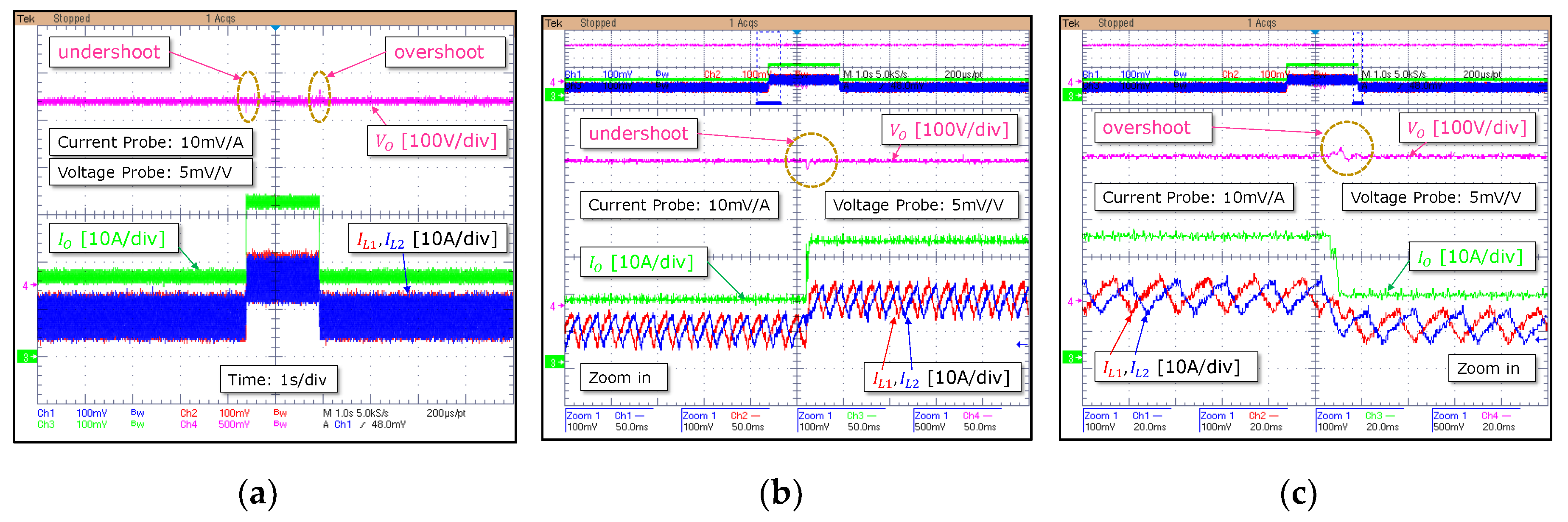
Case 1:
Vin = 70 V,
VO = 140 V,
PO = 0.8 kW →1.6 kW→0.8 kW
Maximum undershoot9.3% V O
(13 V)
11% V O
(16 V)
7% V O
(10 V)
7% V O
(10 V)
−37%
Maximum overshoot10.7% V O
(15 V)
11% V O
(16 V)
7% V O
(10 V)
7% V O
(10 V)
−37%
Maximum settling time11 ms12 ms7 ms7 ms−42%
Case 2:
Vin = 250V,
VO = 385V,
PO = 6 kW →12 kW→6 kW
Maximum undershoot7.8% V O
(30 V)
6.5% V O
(25 V)
5.2% V O
(20 V)
5.2% V O
(20 V)
−20%
Maximum overshoot9.1% V O
(35 V)
7.8% V O
(30 V)
6.2% V O
(24 V)
5.2% V O
(20 V)
−33%
Maximum settling time15 ms20 ms10 ms10 ms−50%

