Hybrid Multimodule DC-DC Converters for Ultrafast Electric Vehicle Chargers


Abstract

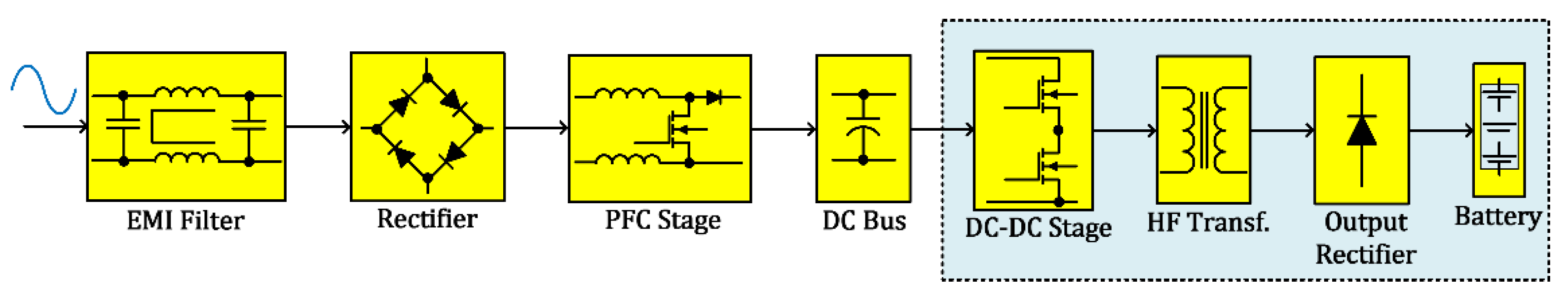
1. Introduction
- Development of a hybrid multimodule DC-DC converter-based DAB topology for EV UFC along with providing generalized small-signal modeling to support the design of the power converter controller. The presented generalized small-signal model of the hybrid multimodule DC-DC converter-based DAB is considered as the primary contribution of this paper.
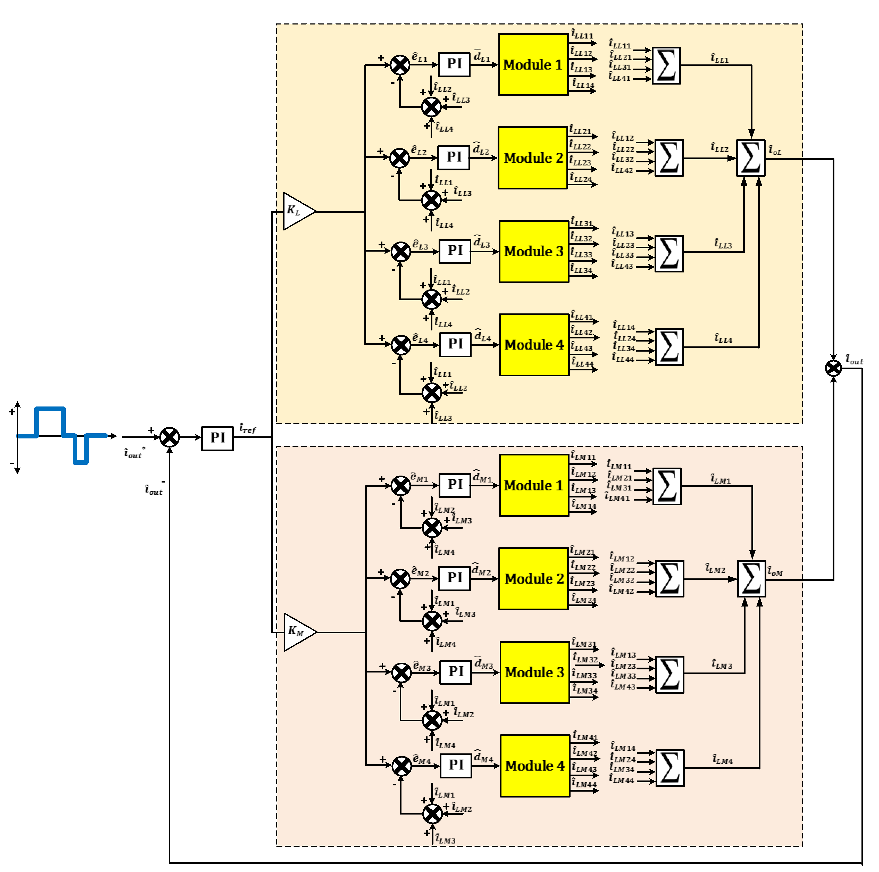
- Examining the cross feedback output current sharing (CFOCS) for the hybrid Input-series output-parallel (ISOP) multimodule power converters to ensure uniform power-sharing among the employed modules and ensure the desired fraction of power handled by each multimodule group.
2. Generalized Small-Signal Analysis for Dual Series/Parallel Input-Output (ISIP-OSOP) Hybrid Multimodule Converters
2.1. Hybrid ISIP-OSOP Generic DC-DC Converter Circuit Configuration
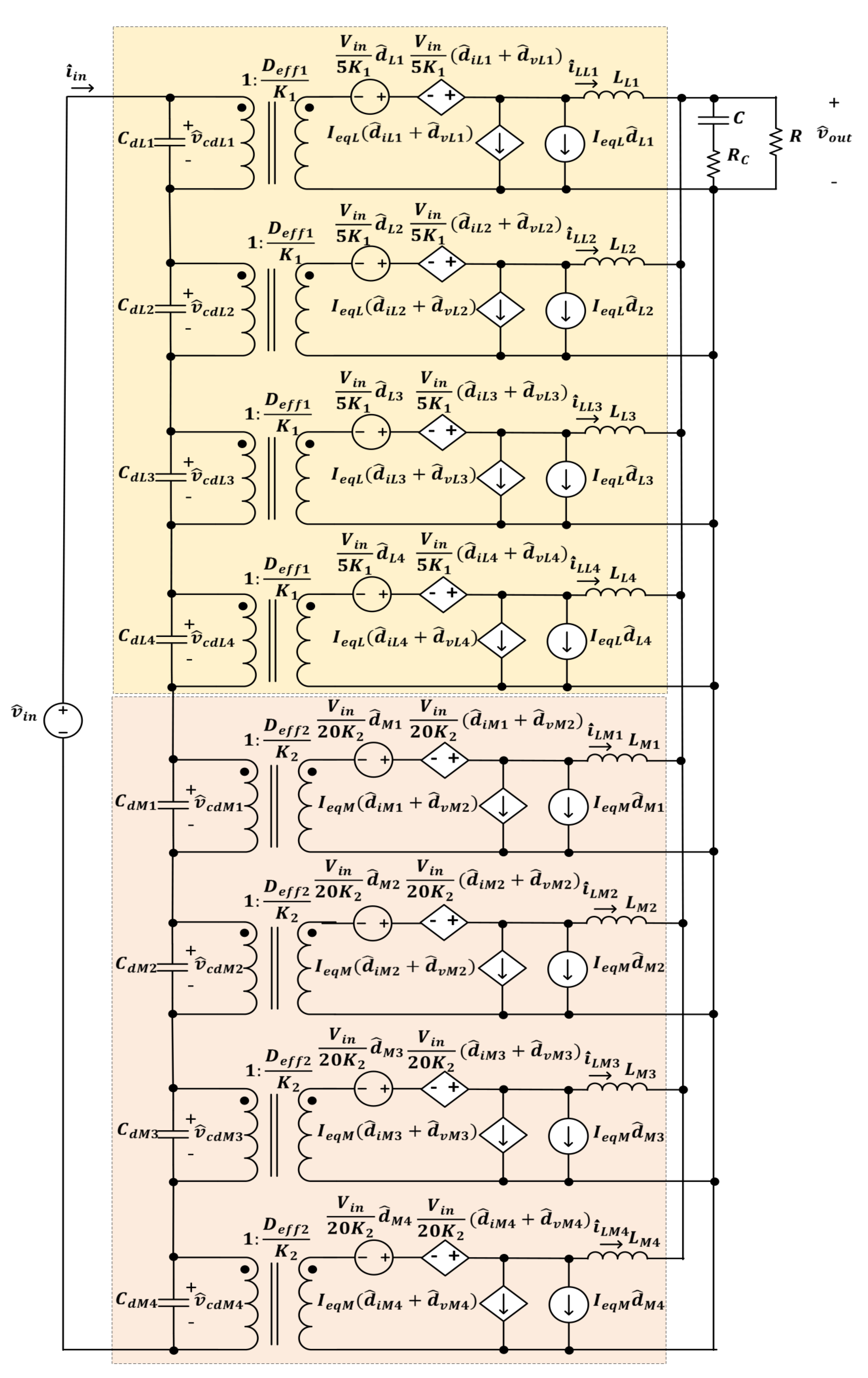
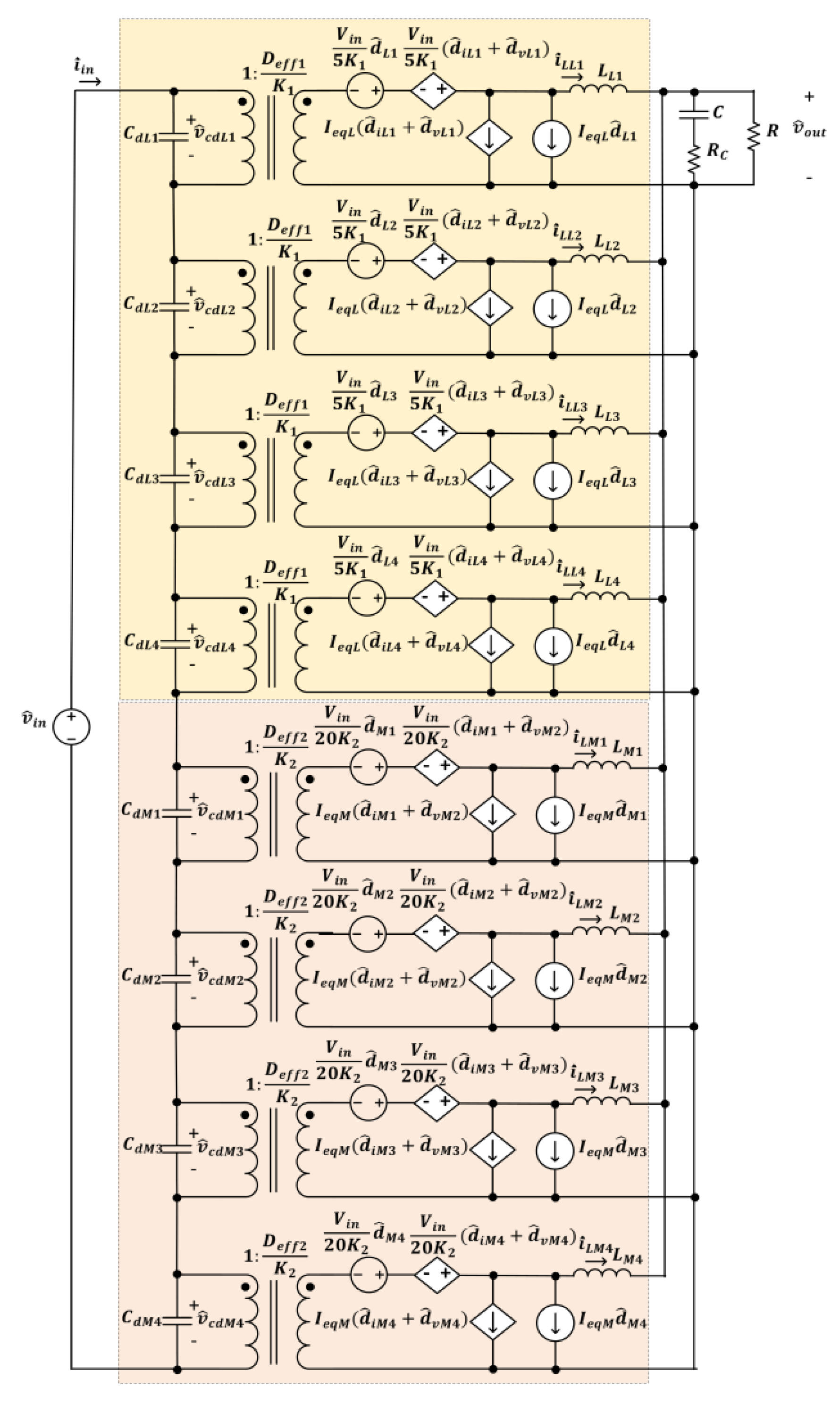
2.2. Hybrid ISIP-OSOP DC-DC Converter Small-Signal Modeling
- , if all the modules in the primary group at the input side are connected in series.
- , if all the modules in the primary group at the input side are connected in parallel or connected in both series and parallel.
- , if all the modules in the primary group at the output side are connected in series.
- , if all the modules in the primary group at the output side are connected in parallel or connected in both series and parallel.
- , if all the modules in the secondary group at the input side are connected in series.
- , if all the modules in the secondary group at the input side are connected in parallel or connected in both series and parallel.
- , if all the modules in the secondary group at the output side are connected in series.
- , if all the modules in the secondary group at the output side are connected in parallel or connected in both series and parallel.
2.2.1. Control-to-Output Voltage Transfer Function
2.2.2. Control-to-Filter Inductor Current Transfer Function
2.2.3. Output Impedance
2.2.4. Converter Gain
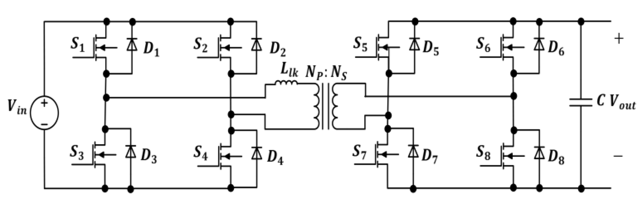
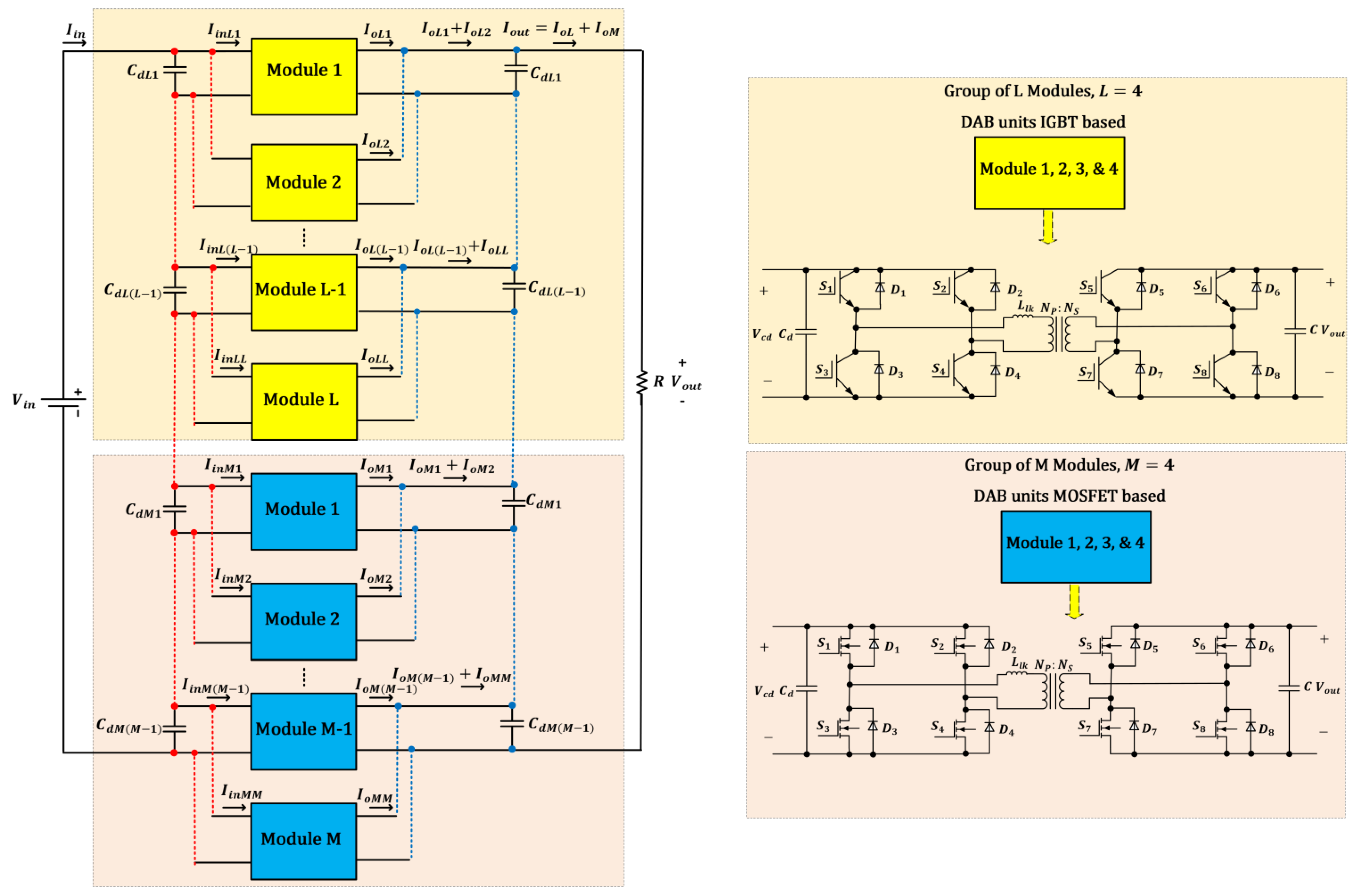
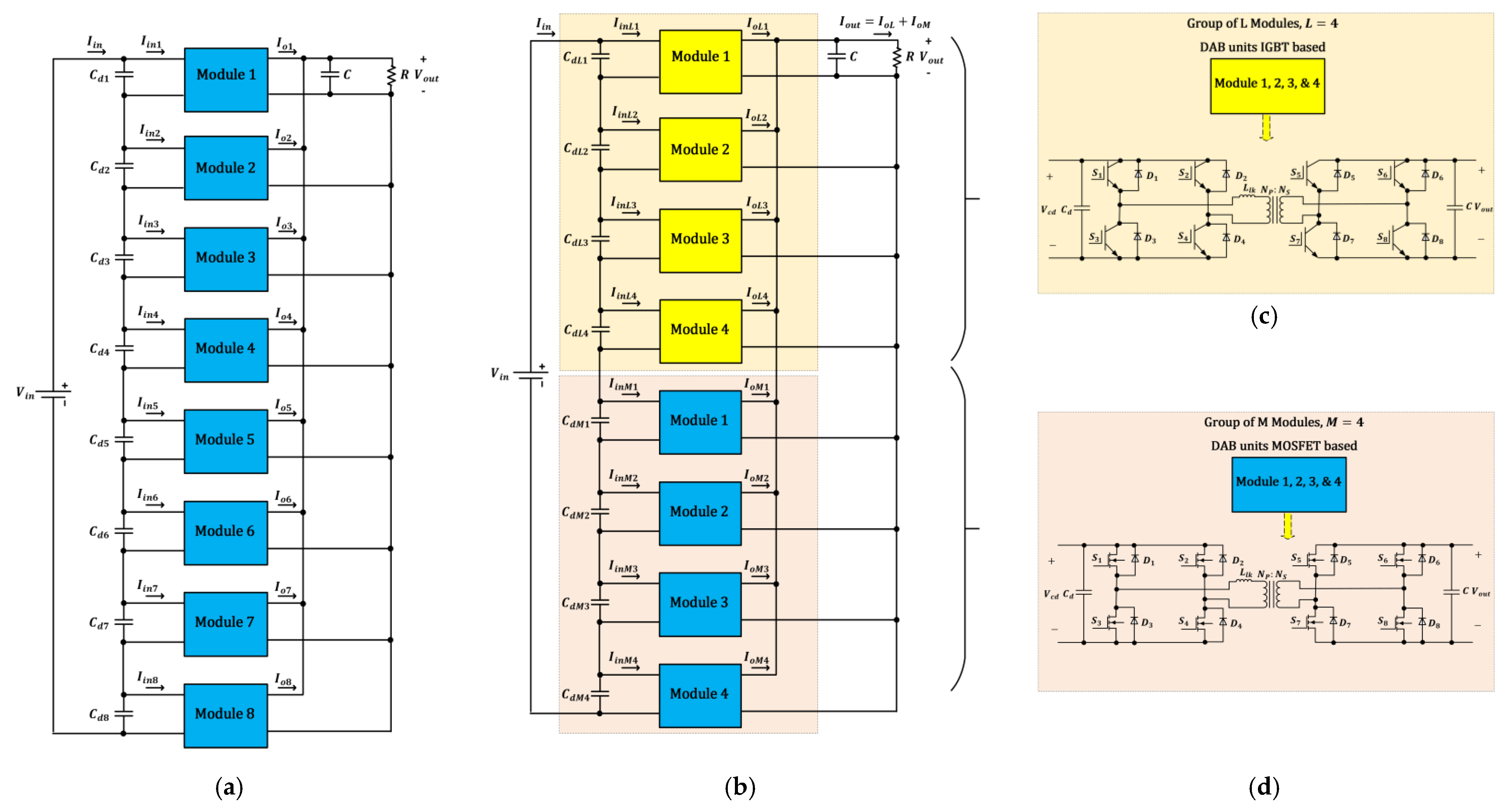
3. Hybrid Input-Series Output-Parallel (ISOP) Multimodule DC-DC Converter
3.1. ISOP Circuit Diagram
3.2. Hybrid ISOP Small Signal Analysis
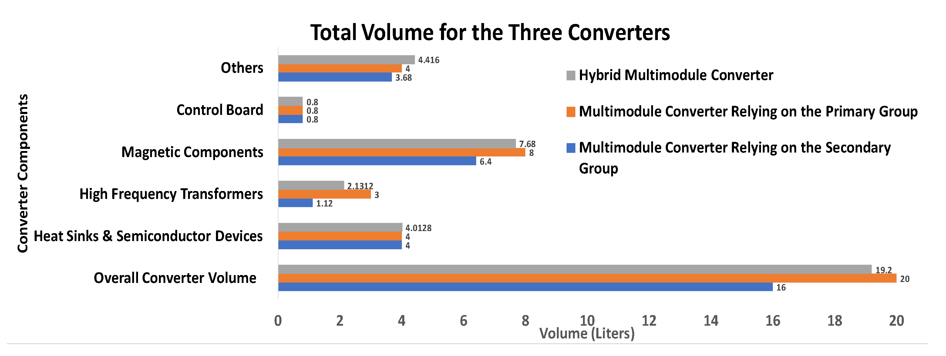
4. Efficiency and Power Density Assessment of the Hybrid Multimodule DC-DC Converter
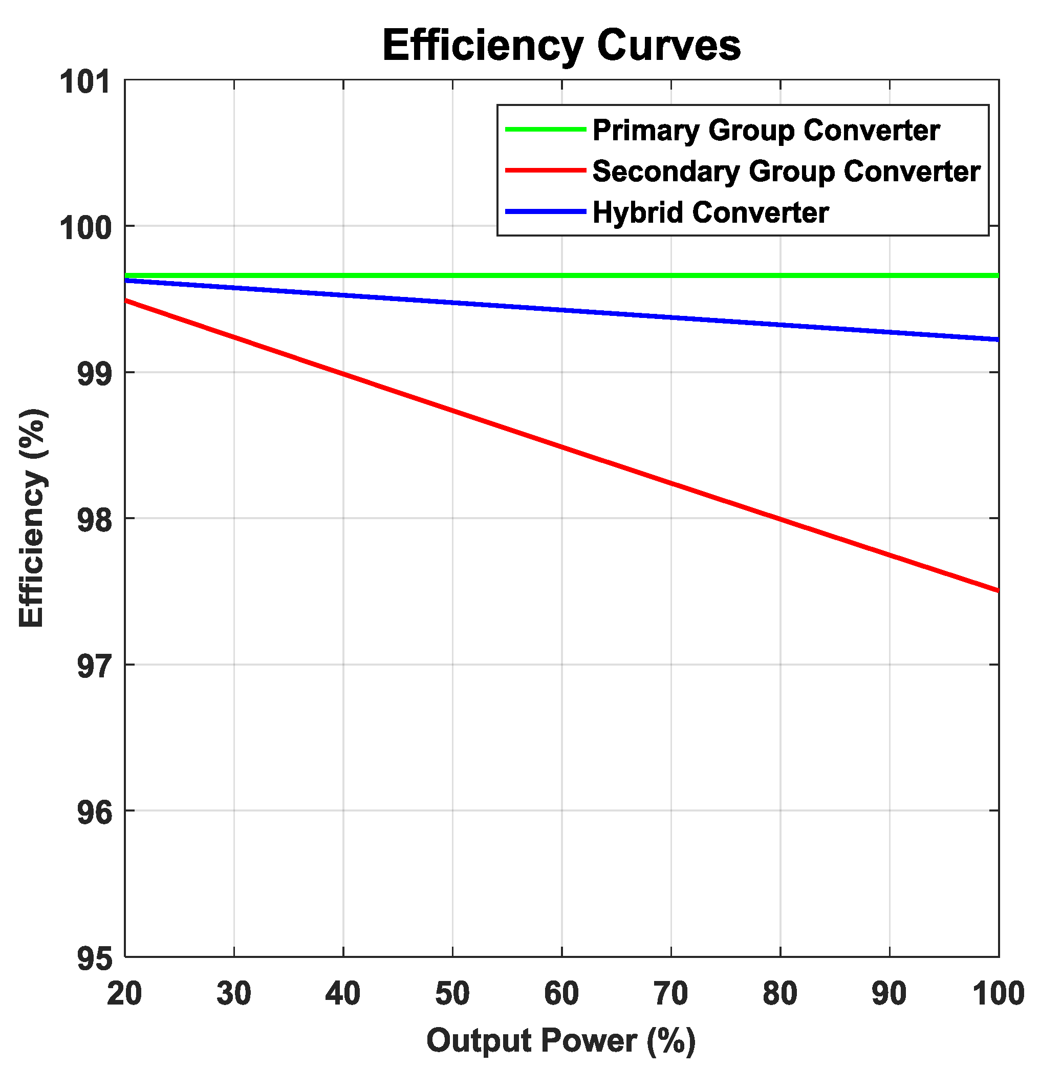
4.1. Efficiency Assessment
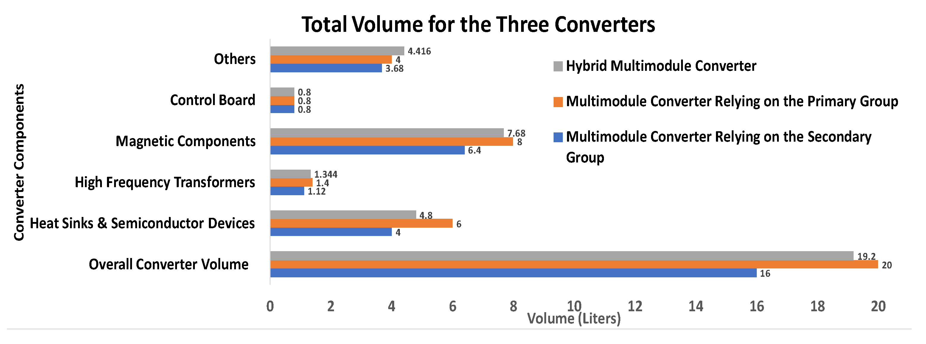
4.2. Power Density Assessment
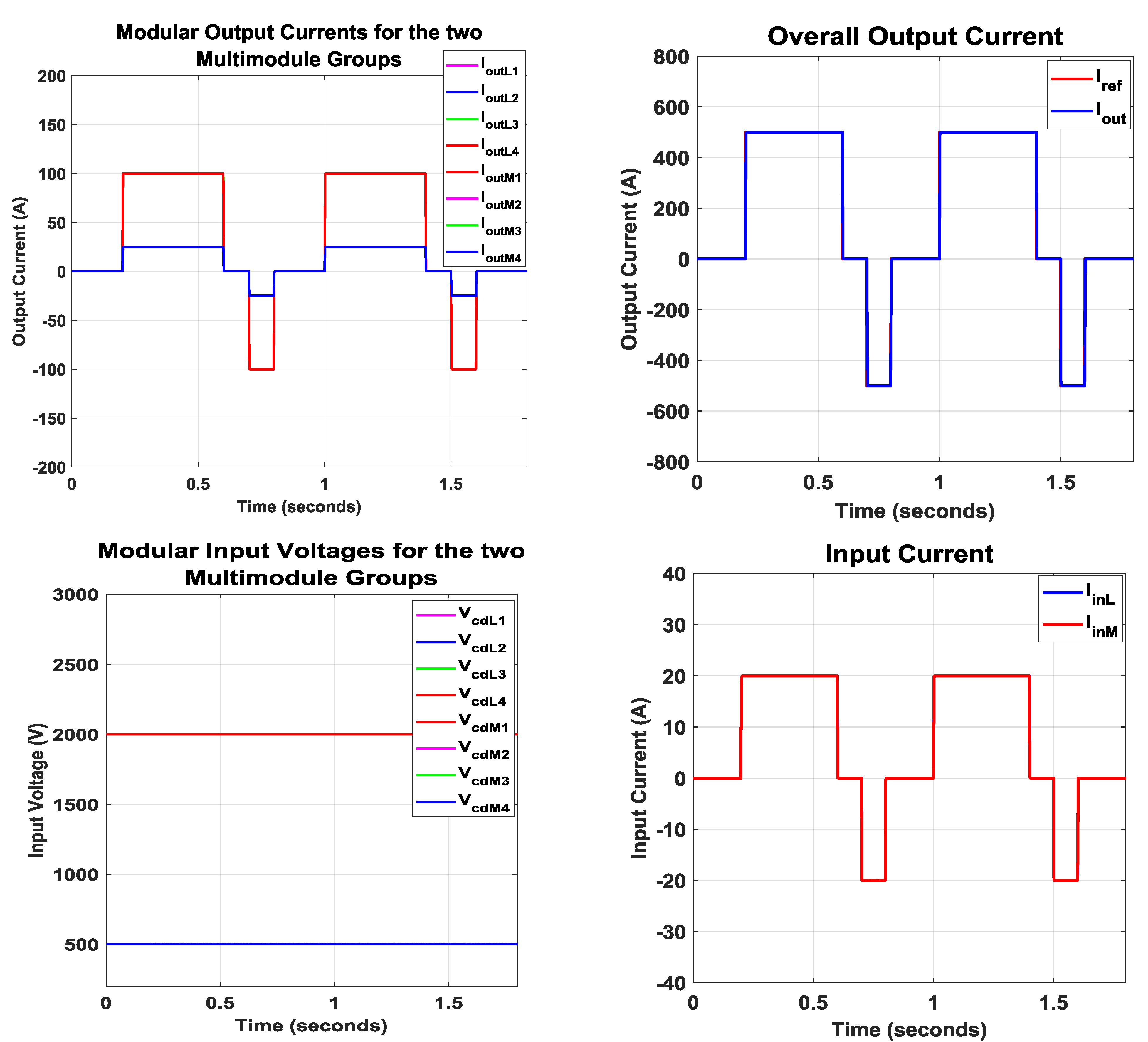
5. Power-Sharing in the Eight-Module Hybrid ISOP Fast Charger DC-DC Converter
6. Discussion
7. Conclusions
Author Contributions
Funding
Acknowledgments
Conflicts of Interest
Abbreviations
| ICEs | Internal Combustion Engines |
| EVs | Electric Vehicles |
| UFC | Ultrafast Charging |
| DAB | Dual Active Bridge |
| DHB | Dual Half Bridge |
| ZVSZ | Zero Voltage Switching |
| CSC | Zero Current Switching |
| CFOCS | Cross Feedback Output Current Sharing |
| ISOP | Input-Series Output-Parallel |
| ISIP-OSOP | Input-Series Input-Parallel Output-Series Output-Parallel |
| ICS | Input Current Sharing |
| IVS | Input Voltage Sharing |
| OCS | Output Current Sharing |
| OVS | Output Voltage Sharing |
References
- Chan, C.C. The State of the Art of Electric, Hybrid, and Fuel Cell Vehicles. Proc. IEEE 2007, 95, 704–718. [Google Scholar] [CrossRef]
- Wilson, J.R.; Burgh, G. Energizing Our Future: Rational Choices for the 21st Century; John Wiley & Sons Inc.: Hoboken, NJ, USA, 2008. [Google Scholar]
- Ehsani, M.; Gao, Y.; Gay, S.E.; Emadi, A. Modern Electric, Hybrid Electric, and Fuel Cell Vehicles: Fundamentals, Theory, and Design; CRC Press LLC: Boca Raton, FL, USA, 2005. [Google Scholar]
- ElMenshawy, M.; Massoud, A. Modular Isolated DC-DC Converters for Ultra-Fast EV Chargers: A Generalized Modeling and Control Approach. Energies 2020, 13, 2540. [Google Scholar] [CrossRef]
- Wang, X.; He, Z.; Yang, J. Electric vehicle fast-charging station unified modeling and stability analysis in the dq frame. Energies 2018, 11, 1195. [Google Scholar] [CrossRef]
- Yang, X.; Li, J.; Zhang, B.; Jia, Z.; Tian, Y.; Zeng, H.; Lv, Z. Virtual Synchronous Motor Based-Control of a Three-Phase Electric Vehicle Off-Board Charger for Providing Fast-Charging Service. Appl. Sci. 2018, 8, 856. [Google Scholar]
- Lv, Z.; Xia, Y.; Chai, J.; Yu, M.; Wei, W. Distributed Coordination Control Based on State-of-Charge for Bidirectional Power Converters in a Hybrid AC/DC Microgrid. Energies 2018, 11, 1011. [Google Scholar] [CrossRef]
- Zhu, Y.; Wang, T.; Xiong, L.; Zhang, G.; Qian, X. Parallel Control Method Based on the Consensus Algorithm for the Non-Isolated AC/DC Charging Module. Energies 2018, 11, 2828. [Google Scholar] [CrossRef]
- Hõimoja, H.; Vasiladiotis, M.; Grioni, S.; Capezzali, M.; Rufer, A.; Püttgen, H.B. Toward Ultrafast Charging of Electric Vehicles; 2012 CIGRE Session: Paris, France, 2012. [Google Scholar]
- Tu, H.; Feng, H.; Srdic, S.; Lukic, S. Extreme Fast Charging of Electric Vehicles: A Technology Overview. IEEE Trans. Transp. Electrif. 2019, 5, 861–878. [Google Scholar] [CrossRef]
- Ronanki, D.; Kelkar, A.; Williamson, S.S. Extreme fast charging technology—Prospects to enhance sustainable electric transportation. Energies 2019, 12, 3721. [Google Scholar] [CrossRef]
- Monteiro, V.; Pinto, J.G.; Ferreira, J.C.; Goncalves, H.; Alfonso, J.L. Bidirectional multilevel converter for electric vehicles. In Proceedings of the 2012 Annual Seminar on Automation, Industrial Electronics and Instrumentation, Guimarães, Portugal, 11–13 July 2012; pp. 434–439. [Google Scholar]
- Yuan, Z.; Xu, H.; Chao, Y.; Zhang, Z. A novel fast charging system for electrical vehicles based on input-parallel output-parallel and output-series. In Proceedings of the 2017 IEEE Transportation Electrification Conference and Expo, Asia-Pacific (ITEC Asia-Pacific), Harbin, China, 7–10 August 2017; pp. 1–6. [Google Scholar]
- Beldjajev, V. Research and Development of the New Topologies for the Isolation Stage of the Power Electronic Transformer. Master’s Thesis, Allinn University of Technology, Tallinn, Estonia, 2013. [Google Scholar]
- Engel, S.P.; Stieneker, M.; Soltau, N.; Rabiee, S.; Stagge, H.; de Doncker, R.W. Comparison of the Modular Multilevel DC Converter and the Dual-Active Bridge Converter for Power Conversion in HVDC and MVDC Grids. IEEE Trans. Power Electron. 2015, 30, 124–137. [Google Scholar] [CrossRef]
- Sari, H.I. DC/DC Converters for Multi-Terminal HVDC Systems Based on Modular Multilevel Converter. Master’s Thesis, Norwegian University of Science and Technology, Trondheim, Norway, August 2016. [Google Scholar]
- Yang, H. Modular and Scalable DC-DC Converters for Medium-/High-Power Applications. Master’s Thesis, Georgia Institute of Technology, Atlanta, GA, USA, 2017. [Google Scholar]
- Fan, H.; Li, H. A high-frequency medium-voltage DC-DC converter for future electric energy delivery and management systems. In Proceedings of the 8th International Conference on Power Electronics—ECCE Asia, Jeju, Korea, 29 May–2 June 2011; pp. 1031–1038. [Google Scholar]
- Papadakis, C. Protection of HVDC Grids Using DC Hub. Master Thesis, Delft University of Technology, Delft, The Netherlands, September 2017. [Google Scholar]
- Carrizosa, M.J.; Benchaib, A.; Alou, P.; Damm, G. DC transformer for DC/DC connection in HVDC network. In Proceedings of the 2013 15th European Conference on Power Electronics and Applications (EPE), Lille, France, 2–6 September 2013; pp. 1–10. [Google Scholar]
- Vasiladiotis, M.; Rufer, A. A Modular Multiport Power Electronic Transformer with Integrated Split Battery Energy Storage for Versatile Ultrafast EV Charging Stations. IEEE Trans. Ind. Electron. 2014, 62, 3213–3222. [Google Scholar] [CrossRef]
- Mortezaei, A.; Abdul-Hak, M.; Simoes, M.G. A Bidirectional NPC-based Level 3 EV Charging System with Added Active Filter Functionality in Smart Grid Applications. In Proceedings of the 2018 IEEE Transportation Electrification Conference and Expo (ITEC), Long Beach, CA, USA, 13–15 June 2018; pp. 201–206. [Google Scholar]
- Tian, Q.; Huang, A.Q.; Teng, H.; Lu, J.; Bai, K.H.; Brown, A.; McAmmond, M. A novel energy balanced variable frequency control for input-series-output-parallel modular EV fast charging stations. In Proceedings of the 2016 IEEE Energy Conversion Congress and Exposition (ECCE), Milwaukee, WI, USA, 18–22 September 2016; pp. 1–6. [Google Scholar]
- De Doncker RW, A.A.; Divan, D.M.; Kheraluwala, M.H. A three-phase soft-switched high-power-density DC/DC converter for high-power applications. IEEE Trans. Ind. Appl. 1991, 27, 63–73. [Google Scholar] [CrossRef]
- Zahid, Z.U.; Dalala, Z.M.; Chen, R.; Chen, B.; Lai, J.-S. Design of bidirectional dc-dc resonant converter for vehicle-to-grid (v2g) applications. IEEE Trans. Transp. Electrif. 2015, 1, 232–244. [Google Scholar] [CrossRef]
- Cui, T.; Liu, C.; Shan, R.; Wang, Y.; Kong, D.; Guo, J. A Novel Phase-Shift Full-Bridge Converter with Separated Resonant Networks for Electrical Vehicle Fast Chargers. In Proceedings of the 2018 IEEE International Power Electronics and Application Conference and Exposition (PEAC), Shenzhen, China, 4–7 November 2018; pp. 1–6. [Google Scholar]
- Srdic, S.; Liang, X.; Zhang, C.; Yu, W.; Lukic, S. A SiC-based high-performance medium-voltage fast charger for plug-in electric vehicles. In Proceedings of the 2016 IEEE Energy Conversion Congress and Exposition (ECCE), Milwaukee, WI, USA, 18–22 September 2016; pp. 1–6. [Google Scholar]
- Justino, J.C.G.; Parreiras, T.M.; Filho, B.J.C. Hundreds kW Charging Stations for e-Buses Operating Under Regular Ultra-Fast Charging. IEEE Trans. Ind. Appl. 2016, 52, 1766–1774. [Google Scholar]
- Everts, J. Modeling and Optimization of Bidirectional Dual Active Bridge AC–DC Converter Topologies. Ph.D. Thesis, KU Leuven, Leuven, Belgium, March 2014. [Google Scholar]
- Marz, M.; Schletz, A.; Eckardt, B.; Egelkraut, S.; Rauh, H. Power Electronics System Integration for Electric and Hybrid Vehicles. In Proceedings of the 6th International Conference on Integrated Power Electronics Systems (CIPS 2010), Nuremberg, Germany, 16–18 March 2010; pp. 1–10. [Google Scholar]
- Emadi, A.; Lee, Y.-J.; Rajashekara, K. Power Electronics and Motor Drives in Electric, Hybrid Electric, and Plug-In Hybrid Electric Vehicles. IEEE Trans. Ind. Electron. 2008, 55, 2237–2245. [Google Scholar] [CrossRef]
- Schoner, H.P.; Hille, P. Automotive power electronics. New challenges for power electronics. In Proceedings of the IEEE 31st Annual Power Electronics Specialists Conference (PESC 2000), Galway, Ireland, 18–23 June 2000; Volume 1, pp. 6–11. [Google Scholar]
- Kolar, J.W.; Drofenik, U.; Biela, J.; Heldwein, M.L.; Ertl, H.; Friedli, T.; Round, S.D. PWM Converter Power Density Barriers. In Proceedings of the Power Conversion Conference (PCC 2007), Nagoya, Japan, 2–5 April 2007; pp. 9–29. [Google Scholar]
- Kolar, J.W.; Biela, J.; Waer, S.; Friedli, T.; Badstuebner, U. Performance Trends and Limitations of Power Electronic Systems. In Proceedings of the 6th International Conference on Integrated Power Electronics Systems (CIPS 2010), Nuremberg, Germany, 16–18 March 2010; pp. 1–20. [Google Scholar]
- Gu, W.-J.; Liu, R. A Study of Volume and Weight vs. Frequency for High-Frequency Transformers. In Proceedings of the IEEE 24th Annual Power Electronics Specialists Conference (PESC 1990), Seattle, WA, USA, 27–30 September 1993; pp. 1123–1129. [Google Scholar]
- Vlatkovic, V.; Sabate, J.A.; Ridley, R.B.; Lee, F.C.; Cho, B.H. Small-signal analysis of the phase-shifted PWM converter. IEEE Trans. Power Electron. 1992, 7, 128–135. [Google Scholar] [CrossRef]
- Lian, Y.; Adam, G.; Holliday, D.; Finney, S. Modular input-parallel output-series DC/DC converter control with fault detection and redundancy. IET Gener. Transm. Distrib. 2016, 10, 1361–1369. [Google Scholar] [CrossRef]
- Ruan, X.; Chen, W.; Cheng, L.; Tse, C.K.; Yan, H.; Zhang, T. Control Strategy for Input-Series–Output-Parallel Converters. IEEE Trans. Ind. Electron. 2009, 56, 1174–1185. [Google Scholar] [CrossRef]
- Lian, Y.; Adam, G.P.; Holliday, D.; Finney, S.J. Medium-voltage DC/DC converter for offshore wind collection grid. IET Renew. Power Gener. 2016, 10, 651–660. [Google Scholar] [CrossRef]
- ElMenshawy, M.; Massoud, A. Multimodule ISOP DC-DC Converters for Electric Vehicles Fast Chargers. In Proceedings of the 2019 2nd International Conference on Smart Grid and Renewable Energy (SGRE), Doha, Qatar, 19–21 November 2019; pp. 1–6. [Google Scholar]
- ElMenshawy, M.; Massoud, A. Multimodule DC-DC Converters for High-Voltage High-Power Renewable Energy Sources. In Proceedings of the 2019 2nd International Conference on Smart Grid and Renewable Energy (SGRE), Doha, Qatar, 19–21 November 2019; pp. 1–6. [Google Scholar]
- Krismer, F.; Kolar, J. Accurate Power Loss Model Derivation of a High-Current Dual Active Bridge Converter for an Automotive Application. IEEE Trans. Ind. Electron. 2010, 57, 881–891. [Google Scholar] [CrossRef]
- Marxgut, C.B. Ultra-Flat Isolated Single-Phase AC-DC Converter Systems. Ph.D. Thesis, Swiss Federal Institute of Technology (ETH Zurich), Power Electronic Systems (PES) Laboratory, Zurich, Switzerland, 2013. [Google Scholar]
- Marxgut, C.; Krismer, F.; Bortis, D.; Kolar, J.W. Ultrafast Interleaved Triangular Current Mode (TCM) Single-Phase PFC Rectifier. IEEE Trans. Power Electron. 2014, 29, 873–882. [Google Scholar] [CrossRef]
- Krismer, F.; Kolar, J.W. Closed Form Solution for Minimum Conduction Loss Modulation of DAB Converters. IEEE Trans. Power Electron. 2012, 27, 174–188. [Google Scholar] [CrossRef]
- Barrera-Cardenas, R.; Molinas, M. A Simple Procedure to Evaluate the Efficiency and Power Density of Power Conversion Topologies for Offshore Wind Turbines. Energy Procedia 2012, 24, 202–211. [Google Scholar] [CrossRef][Green Version]
- Pavlovsky, M.; de Haan, S.W.H.; Ferreira, J.A. Reaching High Power Density in Multikilowatt DC-DC Converters with Galvanic Isolation. IEEE Trans. Power Electron. 2009, 24, 603–612. [Google Scholar] [CrossRef]
- Whitaker, B.; Barkley, A.; Cole, Z.; Passmore, B.; Martin, D.; McNutt, T.R.; Lostetter, A.B.; Lee, J.S.; Shiozaki, K. A High-Density, High-Efficiency, Isolated On-Board Vehicle Battery Charger Utilizing Silicon Carbide Power Devices. IEEE Trans. Power Electron. 2014, 29, 2606–2617. [Google Scholar] [CrossRef]
- Sha, D.; Guo, Z.; Liao, X. Cross-Feedback Output-Current-Sharing Control for Input-Series-Output-Parallel Modular DC-DC Converters. IEEE Trans. Power Electron. 2010, 25, 2762–2771. [Google Scholar] [CrossRef]


| Parameters | Representation | Value |
|---|---|---|
| Primary group | ||
| Input current | if the two groups are connected in parallel at the input side, otherwise | |
| Input voltage | if the two groups are connected in series at the input side, otherwise | |
| Output current | if the two groups are connected in parallel at the output side, otherwise | |
| Output voltage | if the two groups are connected in series at the output side, otherwise | |
| Secondary group | ||
| Input current | if the two groups are connected in parallel at the input side, otherwise | |
| Input voltage | if the two groups are connected in series at the input side, otherwise | |
| Output current | if the two groups are connected in parallel at the output side, otherwise | |
| Output voltage | if the two groups are connected in series at the output side, otherwise | |
| Transfer Functions for an Eight-Module Hybrid ISOP DC-DC Converter | |
|---|---|
| Parameters | Multimodule Converter Relying on the Secondary Group | Multimodule Converter Relying on the Primary Group | Hybrid Multimodule Converter | |
|---|---|---|---|---|
| Primary Group | Secondary Group | |||
| Total rated power | ||||
| Rated power per module | ||||
| Overall input voltage | ||||
| Input voltage per module | ||||
| Total input current | ||||
| Input current per module | ||||
| Overall output voltage | ||||
| Output voltage per module | ||||
| Total output current | ||||
| Output current per module | ||||
| Number of modules | Total of | |||
| Switching frequency | ||||
| Parameters | Primary Multimodule Group | Secondary Multimodule Group | ||||||
|---|---|---|---|---|---|---|---|---|
| Module 1 | Module 2 | Module 3 | Module 4 | Module 1 | Module 2 | Module 3 | Module 4 | |
| Overall converter rated power | ||||||||
| Rated power per module | ||||||||
| Total input voltage | ||||||||
| Input voltage per module | ||||||||
| Overall output voltage | ||||||||
| Module output voltage | ||||||||
| DAB units | ||||||||
| Turns ratio | ||||||||
| Leakage inductance | ||||||||
| Effective duty cycle | ||||||||
| Input capacitance | ||||||||
| Filter inductance | ||||||||
| Filter capacitance | ||||||||
| Resistance | ||||||||
| Switching frequency | ||||||||
© 2020 by the authors. Licensee MDPI, Basel, Switzerland. This article is an open access article distributed under the terms and conditions of the Creative Commons Attribution (CC BY) license (http://creativecommons.org/licenses/by/4.0/).
Share and Cite
ElMenshawy, M.; Massoud, A. Hybrid Multimodule DC-DC Converters for Ultrafast Electric Vehicle Chargers. Energies 2020, 13, 4949. https://doi.org/10.3390/en13184949
ElMenshawy M, Massoud A. Hybrid Multimodule DC-DC Converters for Ultrafast Electric Vehicle Chargers. Energies. 2020; 13(18):4949. https://doi.org/10.3390/en13184949
Chicago/Turabian StyleElMenshawy, Mena, and Ahmed Massoud. 2020. "Hybrid Multimodule DC-DC Converters for Ultrafast Electric Vehicle Chargers" Energies 13, no. 18: 4949. https://doi.org/10.3390/en13184949
APA StyleElMenshawy, M., & Massoud, A. (2020). Hybrid Multimodule DC-DC Converters for Ultrafast Electric Vehicle Chargers. Energies, 13(18), 4949. https://doi.org/10.3390/en13184949