Article

Complex Investigation of High Efficiency and Reliable Heterojunction Solar Cell Based on an Improved Cu2O Absorber Layer

1
Department of Physics, Faculty of Applied Sciences, Polytechnic University of Bucharest, 060042 Bucharest, Romania
2
Academy of Romanian Scientists, 050091 Bucharest, Romania
3
National Institute of Research and Development for Optoelectronics (INOE-2000), 077125 Bucharest, Romania
4
Institute for Energy Technology (IFE), P.O. Box 40, NO-2027 Kjeller, Norway
5
Department of Physics/Center for Materials Science and Nanotechnology (SMN), University of Oslo, P.O. Box 1048 Blindern, N-0316 Oslo, Norway
6
GeePs (Group of electrical engineering—Paris), UMR CNRS 8507, CentraleSupélec, Univ. Paris-Sud, Université Paris-Saclay, Sorbonne Université, 11 rue Joliot-Curie, 91192 Plateau de Moulon, Gif-sur-Yvette CEDEX, France
*
Author to whom correspondence should be addressed.
Energies 2020, 13(18), 4667; https://doi.org/10.3390/en13184667
Submission received: 30 July 2020 / Revised: 27 August 2020 / Accepted: 31 August 2020 / Published: 8 September 2020
(This article belongs to the Special Issue High-Efficiency Crystalline Silicon Solar Cells)

Abstract

:
This study is aimed at increasing the performance and reliability of silicon-based heterojunction solar cells with advanced methods. This is achieved by a numerical electro-optical modeling and reliability analysis for such solar cells correlated with experimental analysis of the Cu2O absorber layer. It yields the optimization of a silicon tandem heterojunction solar cell based on a ZnO/Cu2O subcell and a c-Si bottom subcell using electro-optical numerical modeling. The buffer layer affinity and mobility together with a low conduction band offset for the heterojunction are discussed, as well as spectral properties of the device model. Experimental research of N-doped Cu2O thin films was dedicated to two main activities: (1) fabrication of specific samples by DC magnetron sputtering and (2) detailed characterization of the analyzed samples. This last investigation was based on advanced techniques: morphological (scanning electron microscopy—SEM and atomic force microscopy—AFM), structural (X-ray diffraction—XRD), and optical (spectroscopic ellipsometry—SE and Fourier-transform infrared spectroscopy—FTIR). This approach qualified the heterojunction solar cell based on cuprous oxide with nitrogen as an attractive candidate for high-performance solar devices. A reliability analysis based on Weibull statistical distribution establishes the degradation degree and failure rate of the studied solar cells under stress and under standard conditions.

Graphical Abstract

1. Introduction

Cuprous oxide has attracted much attention for thin film photovoltaic applications due to its high absorption coefficient in the visible region [1]. It is also a nontoxic, low cost material, which is abundant in the Earth’s crust. Cu2O crystallizes in a cubic structure with a lattice constant of 4.269 Å, where the copper (Cu) and oxygen (O) atoms are arranged in face-centered cubic (fcc) and body-centered cubic (bcc) sub-lattices, respectively. Cu2O is a natural p-type semiconductor with a direct band gap of about 2.1 eV, with negatively charged Cu vacancies and O interstitials [2].
Concerning fabrication, cuprous oxide thin films have been prepared by a wide range of synthesis techniques including reactive sputtering, sol–gel technique, plasma evaporation, thermal oxidation, chemical vapor deposition, anodic oxidation, reactive sputtering, electrodeposition, and so on [3]. Wang et al. have demonstrated that the incorporation of nitrogen in thin films can significantly decrease the resistivity [4]. Nitrogen doping in Cu2O has been shown to provide an effective approach to reducing the resistivity/enhancing the hole concentration, as the reported carrier concentrations in N-doped Cu2O thin films are of the order of 1016–1018  cm−3.
Sberna et al. [5] analyzed the effects of nitrogen doping, introduced by ion implantation, on the parameters of Cu2O films. They show that the optimization of structural, optical, and electrical properties of Cu2O thin films synthesized by non-reactive magnetron sputtering can be achieved by post-deposition thermal annealing in oxygen atmosphere.
Foremost among the challenges in metal oxide solar cells development are the improvement of the performance and reliability of these devices. A potential candidate for high-efficiency metal oxide solar cells, such as the Cu2O/ZnO/c-Si tandem heterojunction solar cell, could theoretically reach a conversion efficiency above 30% [6]. The key to achieving higher efficiencies for solar cells made from these materials is to tune the optical and electrical properties of absorber material in the solar cell, such as cuprous oxide (Cu2O).
The conversion efficiency for the current ZnO/Cu2O heterojunction solar cells is around 8%, while the potential is 14% conversion efficiency. Factors like low power conversion efficiency, high defect density, and large conduction band offset for the metal oxide heterojunction imply that there is room for research to further optimize the device. Probe-scanning instruments can provide valuable information towards the characterization and optimization of solar cell layers. However, interface defect states pose a challenge in reaching efficiencies close to the theoretical maximum. Currently, the conversion efficiency for cuprous oxide heterojunctions has the potential to reach 14% as reported by Takiguchi et al. [7] and a theoretical maximum efficiency of around 19%.
The present study is based on numerical electro-optical modeling and reliability analysis and is dedicated to increasing the performance and reliability of heterojunction solar cells [8,9,10]; it is correlated with the experimental investigation (morphological, structural, and optical) of an improved Cu2O absorber layer. Its morphological and structural characterization is based on SEM, AFM, and XRD analyses [11]. The optical characterization of the Cu2O layer uses FTIR spectroscopy and SE analyses [12]. Furthermore, a statistical reliability study is carried out, analyzing the lifetime, degradation degree, and failure rate of the studied solar cells.

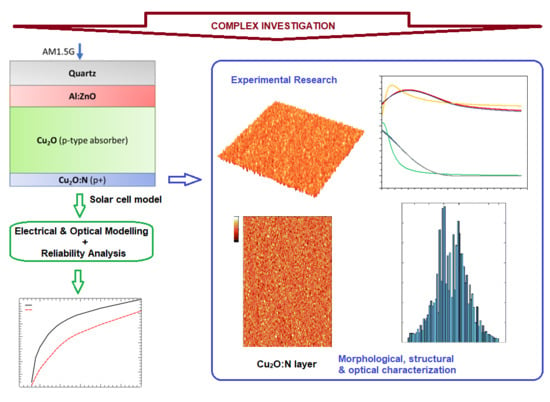
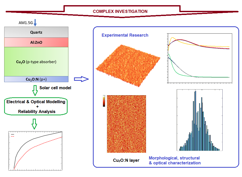
2. Numerical Modeling of Cu2O Heterojunction Solar Cell

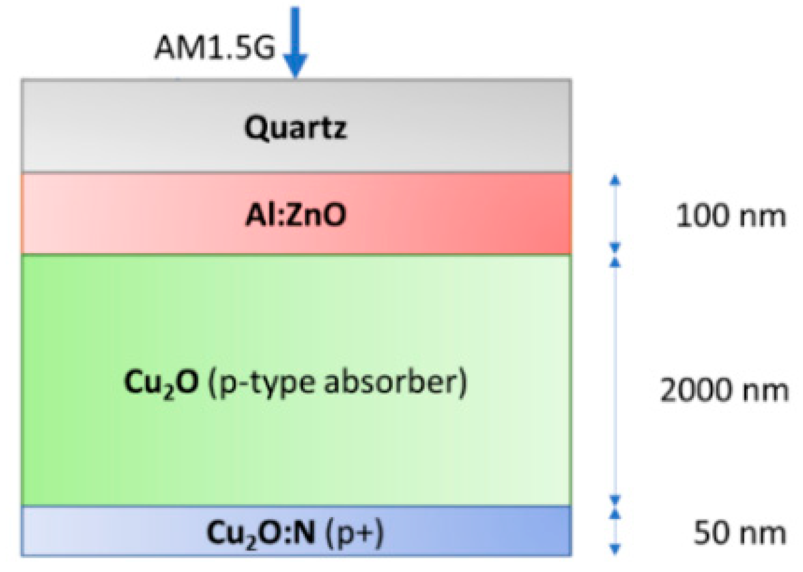
2.1. Diagram of the Solar Cell Simulation Model

A schematic representation of the Cu2O heterojunction solar cell simulation model is shown in Figure 1. The device structure includes a quartz glass superstrate, an aluminum-doped ZnO (AZO) n+ emitter layer, a Cu2O p-type absorber layer, and a bottom Cu2O:N layer.

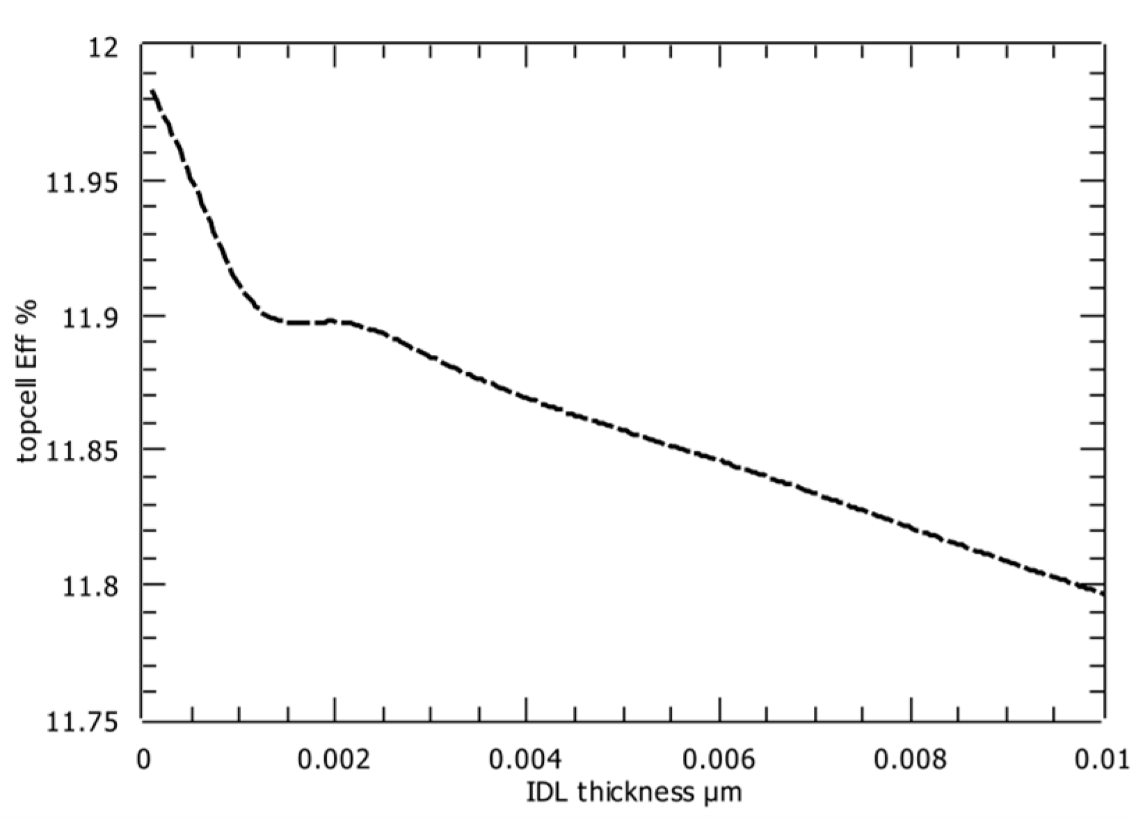
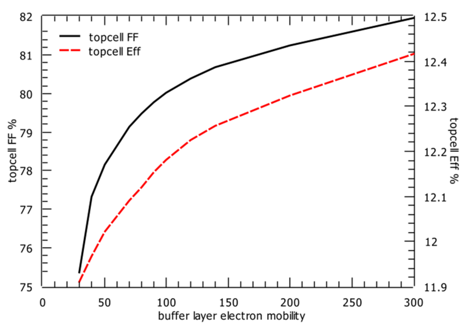
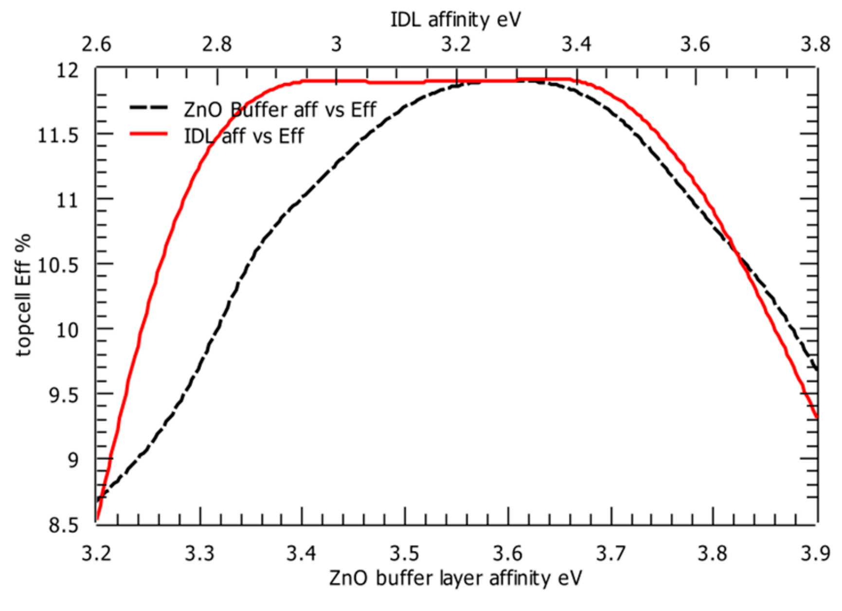
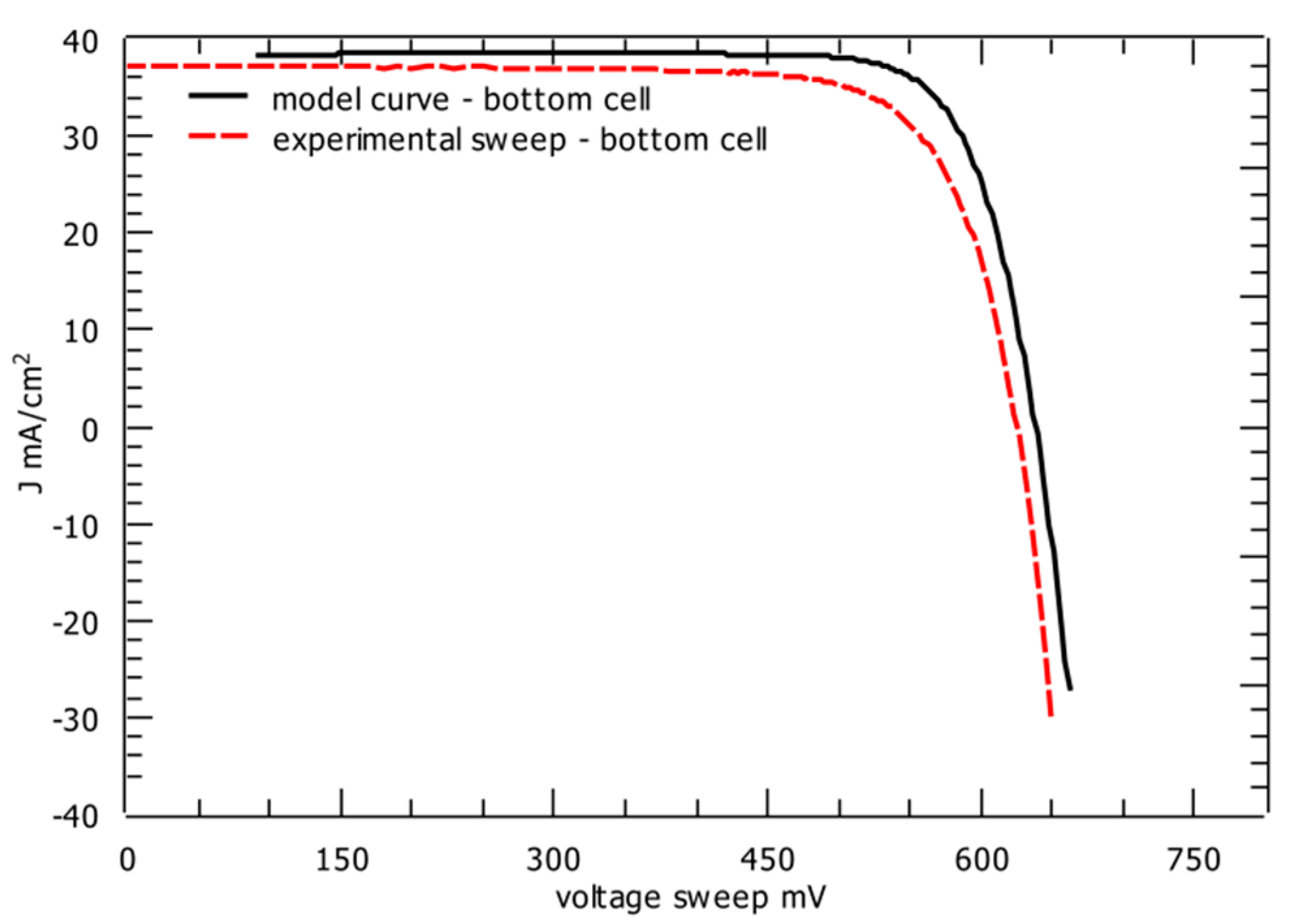
2.2. Electrical Modeling and Simulation Results for the Two Subcells of the Tandem Heterojunction Solar Cell

Numerical modeling of the metal oxide heterojunction solar cell was developed based on three simulation software packages, namely Silvaco Atlas, MATLAB, and Quokka 2. The tandem heterojunction solar cell was constituted from two subcells: the metal oxide (Cu2O) top subcell and c-Si bottom subcell. The electrical properties of the absorber (Cu2O) and buffer layer (ZnO) from the structure of the top subcell were analyzed using Silvaco Atlas software. The implementation of defects, as well as the study of two efficient materials (ZnO and Ga2O3) for the buffer layer were investigated [13,14,15,16,17] and several analyses were considered using the Takiguchi model [7]. A transition interface defect layer (IDL) was introduced as well.
Several comparisons using the Silvaco numerical model were discussed. One of the most interesting buffer materials is ZnO generally, and in particular, the AZO layer (Al:ZnO). This material is very suitable from the point of view of the conduction bandgap offset in regards to Cu2O. The dependence of the AZO thickness on top cell efficiency is plotted in the Figure 2; the optimum value for the AZO thickness looks to be 0.25 µm. Further analysis examined (1) the dependence of IDL thickness on top cell efficiency (Figure 3), (2) the impact of buffer electron mobility on subcell fill factor (FF) and efficiency (η) (Figure 4), and (3) the impact of buffer and IDL affinity on subcell efficiency (η) (Figure 5). We have remarked that a buffer electron mobility value under 100 cm2/V⋅s would greatly affect the fill factor and efficiency. Defect densities are very important from the practical point of view in order to obtain required performance, especially for absorber and defect layers. We could compare different buffer and IDL materials from the point of view of their affinity. The optimal affinity interval (3.4–3.6 eV) for the buffer layer would determine the lower conduction band offset with the copper oxide absorber layer. The optimal affinity interval for IDL is larger (from 2.95 to 3.4 eV).
A numerical model was adopted using the Quokka 2 software for the bottom subcell. The current-voltage (J-V) characteristics compared the experimental curve with the numerical modeled one (Figure 6).
The numerical model was used to fit to the experimental curve for control and prediction (Table 1) and to establish the essential electrical parameters for the silicone solar subcell.
A comparison between the experimental graph and Quokka modeled one for EQE (external quantum efficiency) is presented in Figure 7. Further improvement of the model would be required in the interval 750–1000 nm.
The rather large current mismatch between the two subcells in tandem configuration, caused by the large band gap difference for the two absorbers, allows for individual optimization of the top and bottom subcells and favors the arrangement of a four-terminal configuration.
That is why it is possible to increase the conversion efficiency of the tandem heterojunction ZnO/Cu2O silicone solar cell beyond the limit of conventional c-Si single-junction solar cell.

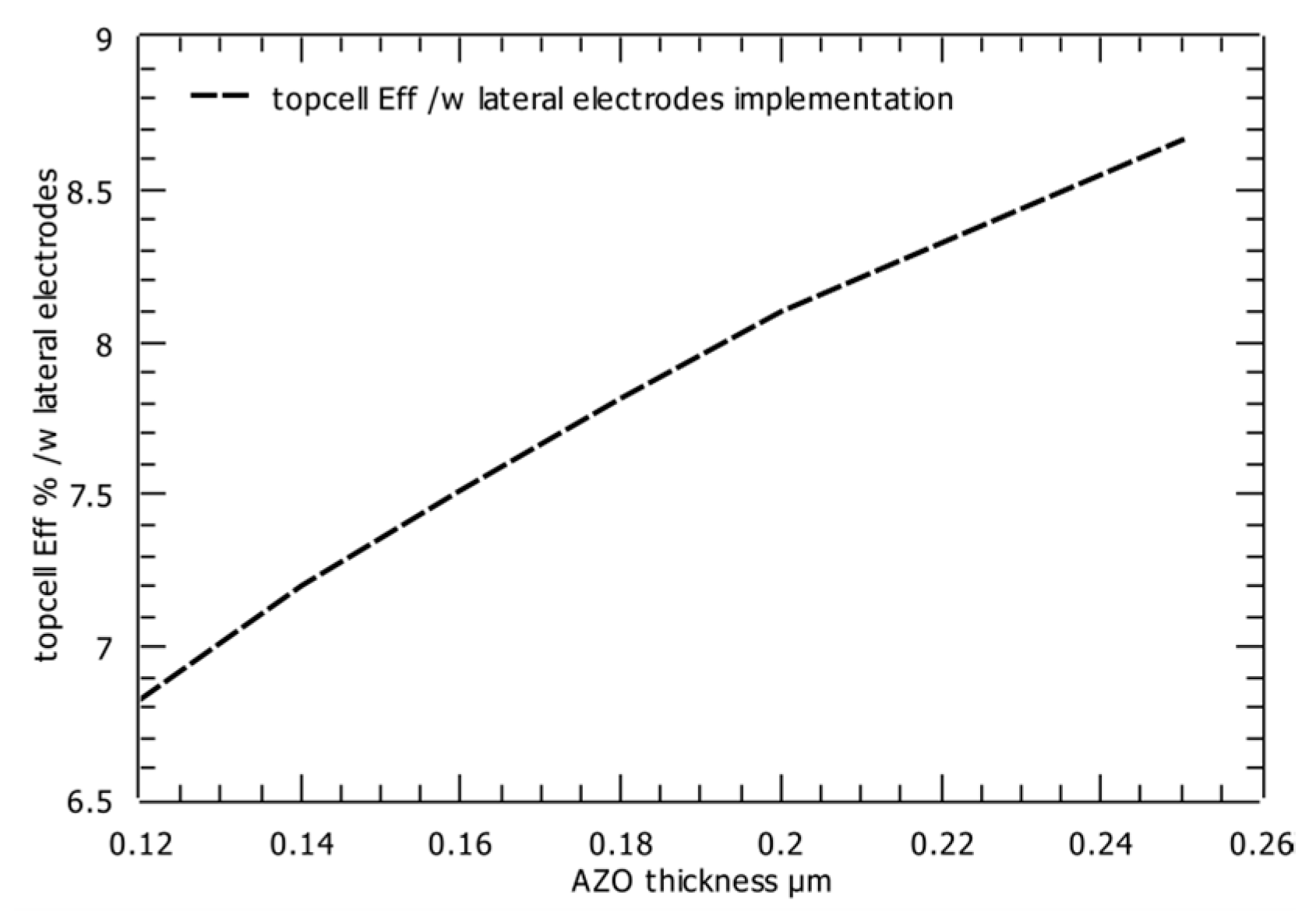
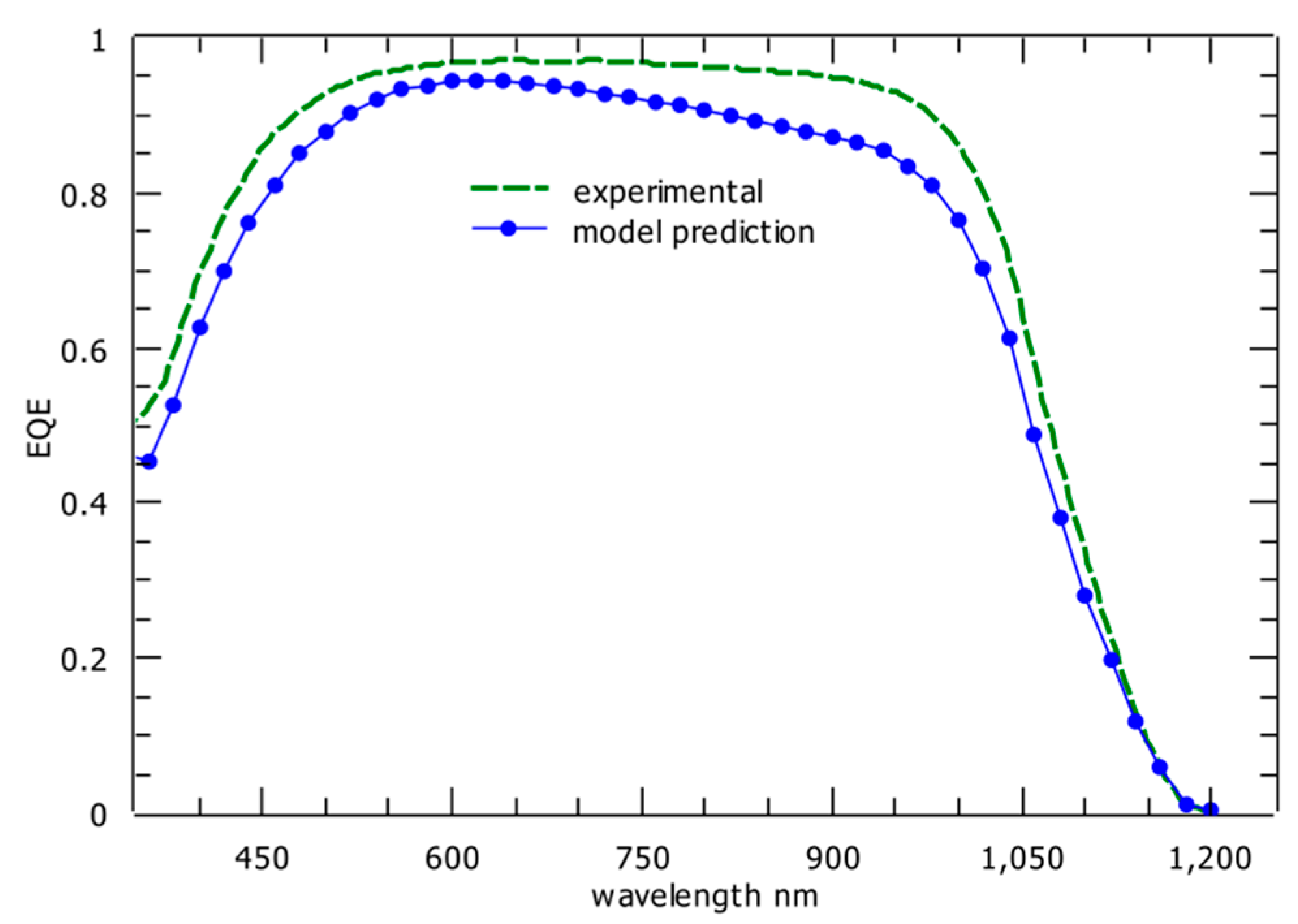
2.3. Optical Modeling and Simulation Results for the Top Subcell

In order to evaluate the optical characteristics of the device, we have used OPAL 2 software developed by PV (photovoltaic) Lighthouse [18]. OPAL 2 is a fast, reliable, and free online software tool that simulates the optics of advanced solar cells [19,20]. The optical modeling was performed for an AM1.5G solar spectrum and with experimentally determined complex refractive indices for the AZO and Cu2O layers. The modeling was performed in the wavelength range from 300 nm to 800 nm.
Simulated optical functions were the normalized reflectance, absorptance, and transmittance as a function of wavelength for the studied device model, for the samples 1–3 of Cu2O: N, to be discussed in the experimental section. The simulations are presented in Figure 8. For these simulations, a 100 nm thick AZO layer, a 2 μm thick Cu2O layer, and a 50 nm thick Cu2O:N layer were implemented in the model. A standard thickness of 50 nm was set for samples 1–3 of Cu2O:N used in the solar cell structure.
The maximum reflectance in the 575–800 nm wavelength range for Sample 2 is a bit lower than the maximum values for Samples 1 and 3, as can be seen in Figure 8a. This result could prove useful for reflectance loss optimization.
The absorptance is high for all samples in the 300–525 nm wavelength range (with an average value of 90%). It decreases abruptly in the 525–600 nm range and tends to low values (<10%) in the 600–800 nm range, as seen in Figure 8b.
Transmittance was plotted concurrently for all three samples, as shown in Figure 8c. The transmittance suggests that Samples 1 and 3 yield a better transmission starting from the 560 nm wavelength. The cutoff wavelengths from the transmittance plot are 595 nm, 620 nm, 650 nm, 690 nm, 730 nm, 775 nm, and so on, a periodic spectral pattern being observed. The same approach can be taken for the reflectance plot. For the absorptance plot, the only significant cutoff wavelength is 590 nm. Based on the transmittance data, Tauc plots [20] for Samples 1–3 were calculated and presented in Figure 9.
Tauc plots indicate an optical bandgap around 2.18 eV for Sample 1, 2.17 eV for Sample 2, and around 2.18 eV for Sample 3, which is in agreement with the ellipsometry measurements (see experimental section).

2.4. Relevance of the Best Simulation Tools for Numerical Modeling and Optimization of Metal Oxide Solar Devices

The simulation methodology could be used for design and material performance optimization. Two simulators were considered to be the best for the two subcells; Silvaco is the optimum tool for the top metal oxide solar subcell and absorbs the high energy part of sunlight, while PC1D is the most efficient tool for the bottom silicone solar subcell and absorbs the low energy part of sunlight. The simulated device with optimized parameters could be validated by comparing the numerical modeled results and performance with the experimental ones offered by an industrial manufactured solar cell with identical parameters.

3. Experimental Investigation of N-Doped Cu2O Absorber Layer

3.1. Cu2O Thin Film Fabrication and Overall Characterization

Cu2O thin films were deposited on quartz substrates by direct current (DC) magnetron sputtering system (Semicore Triaxis) on 1 cm × 1 cm quartz substrates at 400 °C by varying the N2 and Ar/O2 flow [21]. Samples 1 and 2 were deposited at 400 °C with nitrogen flows 1 and 3 sccm (standard cubic centimeters per minute), respectively, while the Ar/O2 flow was maintained constant. Sample 3 was deposited at 400 °C with Ar/N2 flow of 1 sccm while the O2 flow was fixed. The pre-sputtering time was 15 min, to avoid any contamination. The quartz substrates were cleaned in piranha solution and rinsed in deionized water, blown dry with nitrogen, and loaded into the deposition chamber. The same deposition time was used for all samples. The deposition power was fixed at 100 W. The base pressure before deposition was below 5 × 10⁻⁷ Torr while the sample stage was rotated at a constant speed of 12 rpm during deposition. The Hall effect measurements (LakeShore 7604) using the van der Pauw method were carried out to determine the hole mobility, resistivity, and hole carrier density.
The hole carrier density of as-deposited Sample 0 is ~1015 cm−3 with low mobility (~13 cm2/Vs) and resistivity (~200 Ωcm), respectively. The hole carrier density for Samples 1 and 2 varied from ~1017–1019 cm−3 with low carrier mobility (~0.1–1 cm2/Vs) and resistivity (3–13 Ωcm), respectively, while Sample 3 has carrier density ~1016 cm−3 with resistivity ~54 Ωcm and carrier mobility ~1.5 cm2/Vs. A reduced resistivity was achieved in the N-doped samples (1, 2, and 3) compared to the undoped Sample 0. This may reflect the presence of N in the DC Cu2O film magnetron sputtering process influencing the electrical characteristics of solar cell as mentioned previously.
The process characteristics and layer structure of Cu2O:N thin film samples, deposited by DC magnetron sputtering on quartz substrate, are presented in Table 2.

3.2. Morphological and Structural Characterization of the Cu2O:N Films

The surface morphology of the Cu2O:N thin films was studied by SEM with the Quanta Inspect F 50 scanning electron microscope. Topographic AFM imaging was also performed by AFM with the Veeco Innova atomic force microscope, in the tapping mode, with 2.5 μm/s scanning speed. AFM images have a resolution of 512 × 512 pixels. The software used for image analysis was SPM Lab Analysis v.7.0 (Version 7.0, Veeco Innova, Bruker-Milton, ON, Canada, Santa Barbara-CA, USA.)

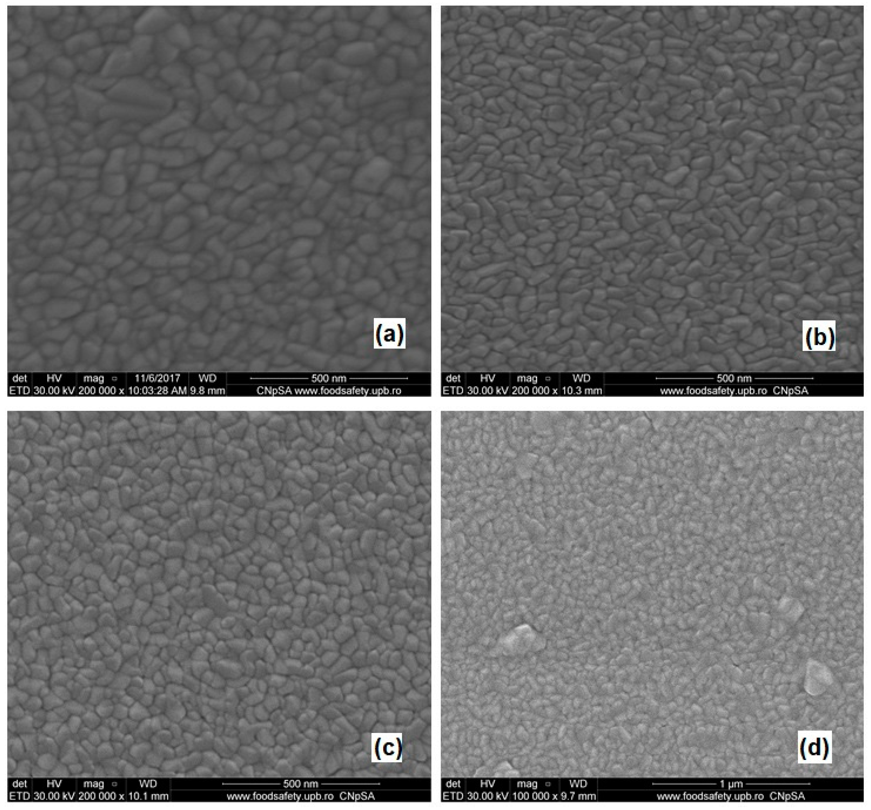
3.2.1. Scanning Electron Microscopy (SEM)

Experimental measurements for the determination of surface morphology were performed on Cu2O:N thin films deposited by the DC magnetron sputtering on the quartz substrate under different gas flow conditions. Figure 10 shows the SEM images of four samples (see Table 2): one undoped Cu2O film (Sample 0) and three Cu2O:N thin film samples (Samples 1–3).
The grain size in the deposited layers is listed in Table 2 and compared with undoped Cu2O film (Sample 0). With the increase of the N2 flow, the films display a uniform layer surface with larger particle size (Samples 1 and 2). A varied Ar pressure induces a non-uniform particle size distribution (Samples 1 and 3). The particle size distribution of the undoped Cu2O layer is non-uniformly distributed in the range 20–90 nm. As result, the presence of N2 and an Ar/O2 fixed flow improves the size uniformity of the deposited Cu2O layers.

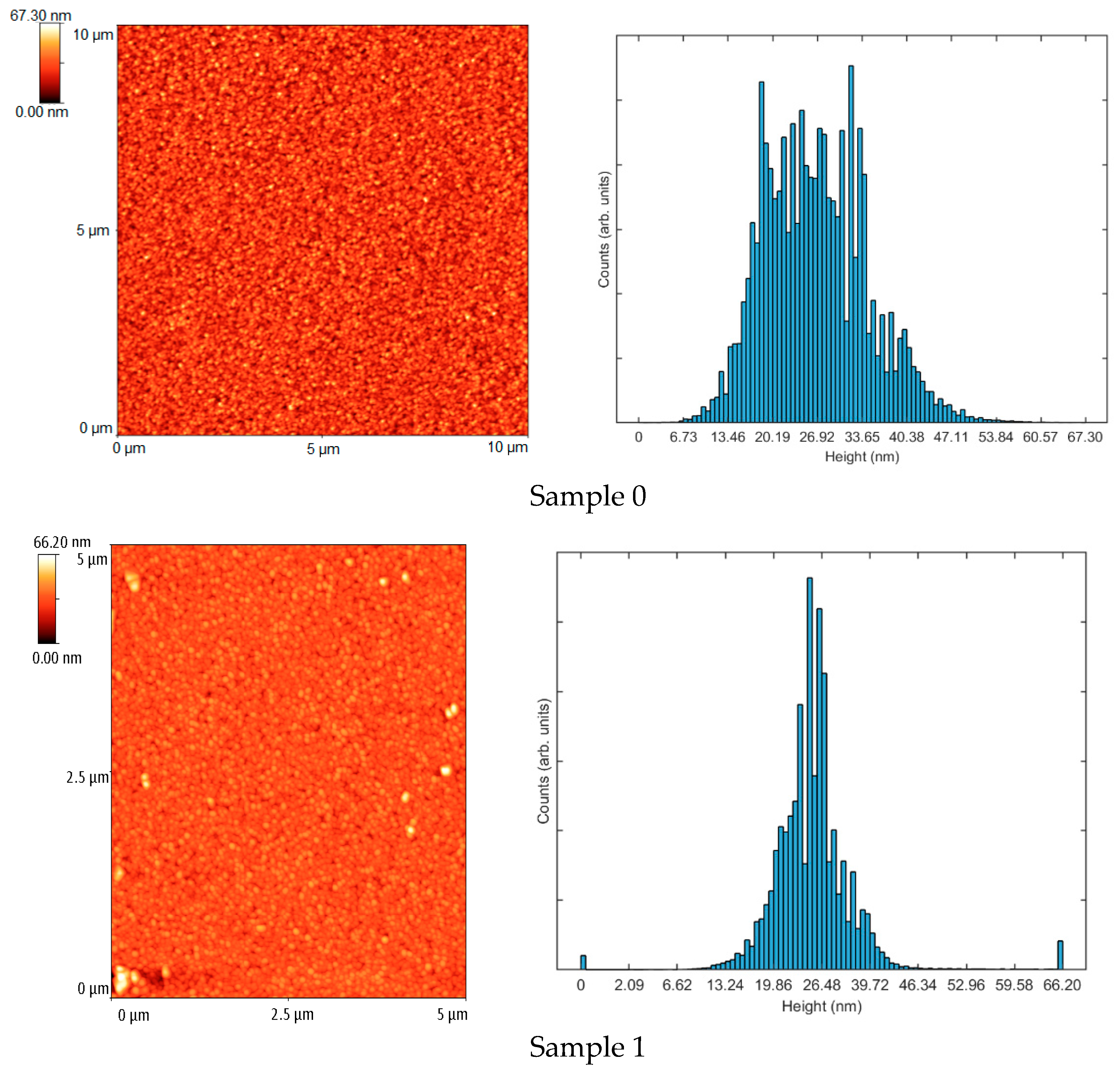
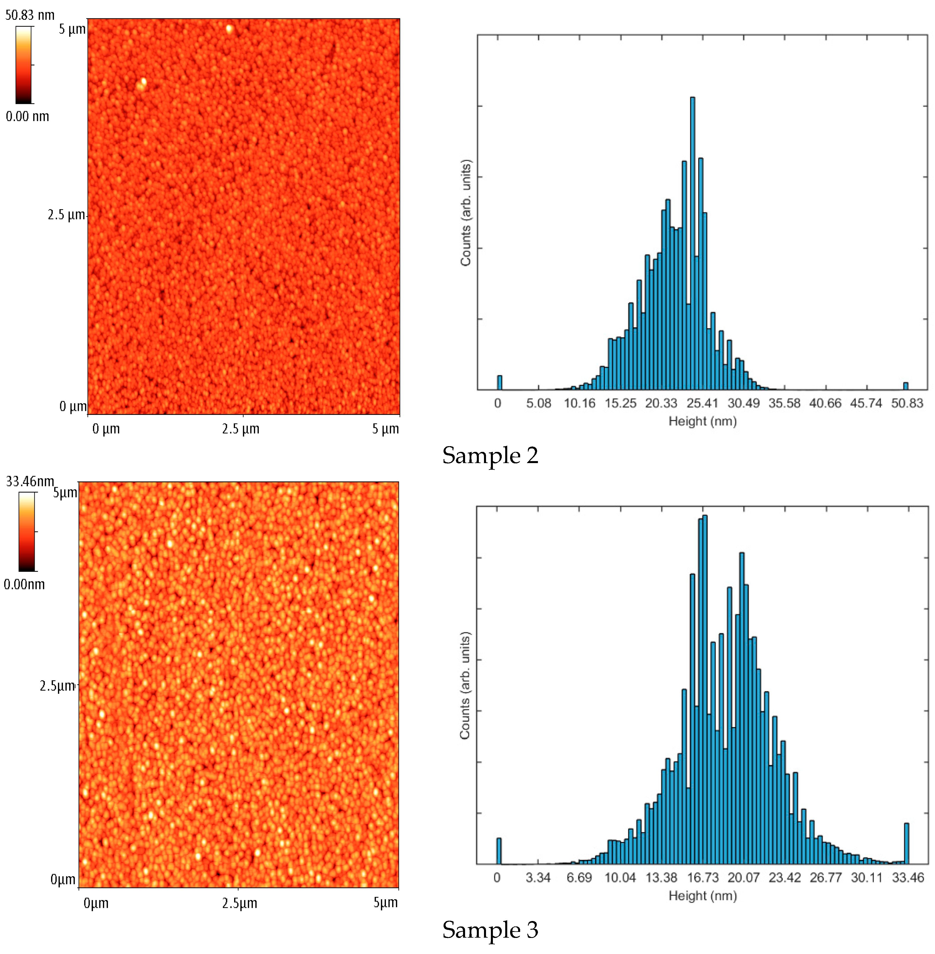
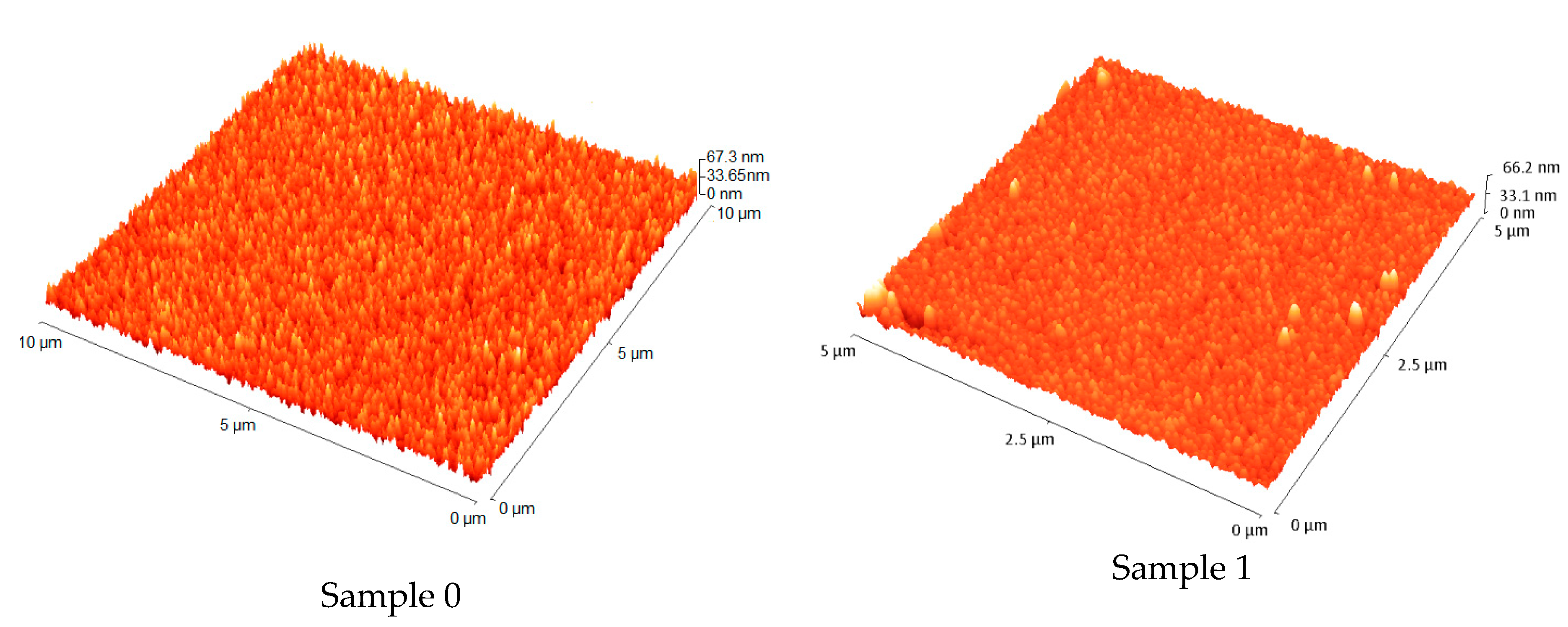
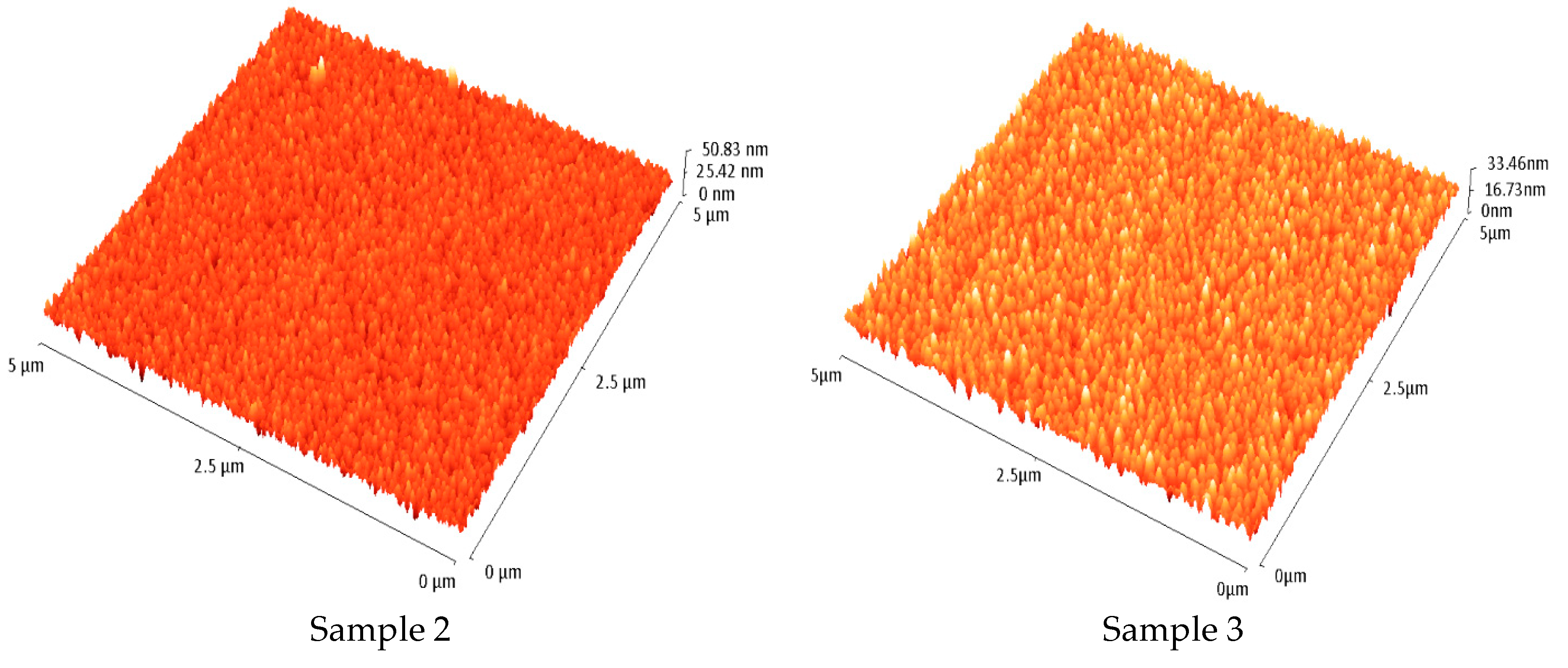
3.2.2. Atomic Force Microscopy (AFM)

The grain size, including surface roughness of Cu2O:N thin film deposited on quartz substrate, was measured by topographic AFM imaging. The surface morphologies for each of the N-doped thin film samples compared with Sample 0 are shown in Figure 11 as 2D AFM images, along with their corresponding surface profile histograms, and in Figure 12 as 3D AFM images. The root-mean-square surface roughness (RRMS) for each sample was extracted from their AFM images [22,23].
The histograms represent the statistical distribution of the height surface profile of the Cu2O samples derived from the AFM images and show a higher distribution in the first half of the height range for Samples 1 and 2. However, the height profile distribution of Sample 3 shows less roughness. This is related to the deposition conditions and in accordance with the RRMS parameter calculations in Table 3, which shows a lower RRMS for this sample. According to the statistical distribution of the surface height profile, Samples 1, 2, and 3 have the highest frequency at a surface height of 26 nm, 25 nm, and 17 nm, respectively. For validation, RRMS was derived from the histograms based on the 2D AFM images, processed in MATLAB, and presented in Table 3.
According to Table 3, the roughness deviation values follow the same trend as the RRMS values, where Sample 1 has the highest deviation and Sample 3 presents the lowest one. Additionally, the undoped Cu2O film (Sample 0) presents a greater roughness than the doped Samples 1–3.

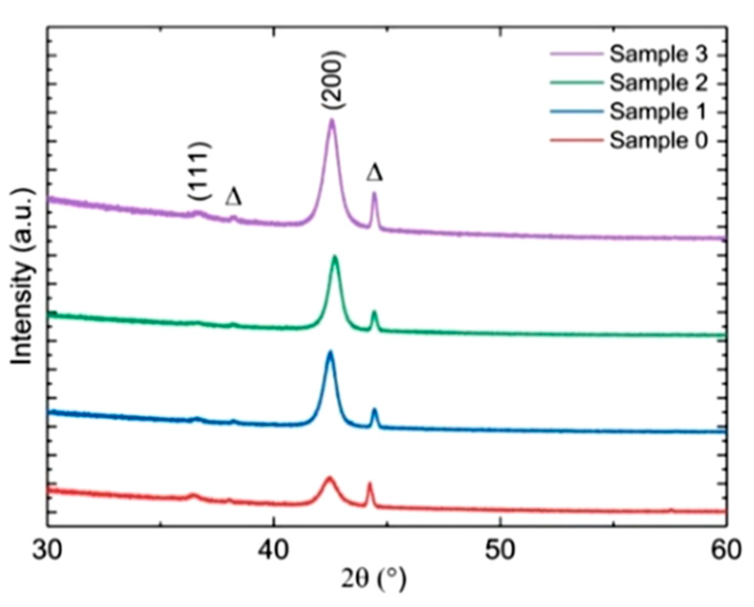
3.2.3. Structural Characterization by XRD

The XRD pattern was obtained by a Bruker AXS D8 Discover Diffractometer, using Cu Kα-radiation and a Bragg–Brentano configuration. The background and Kα2 were stripped from the XRDs using the EVA software. The dominant XRD peaks were recorded in 2-theta range from 30–60°.
Figure 13 displays the XRD patterns of all samples, recorded in the range 30–60°. XRD patterns show that all films were dominated by a (200) reflection peak at 42.61° and a (111) reflection peak corresponding to 36.45°. The XRD pattern is not significantly influenced by nitrogen doping [24]. The Cu2O peaks were determined by comparing experimental XRD peak patterns with the standard Powder Diffraction cards (ICDD patterns: 01-071-3645) [25].
XRD patterns of the Cu2O:N films prepared under various N2 flow rates, together with the data of the Cu2O reference films, show highly oriented (111) planes. For the Cu2O:N samples, the peak intensity of the (111) plane decreases significantly with increasing of N2 flow rate, and (200) planes show up in the heavy N-doping range [26].

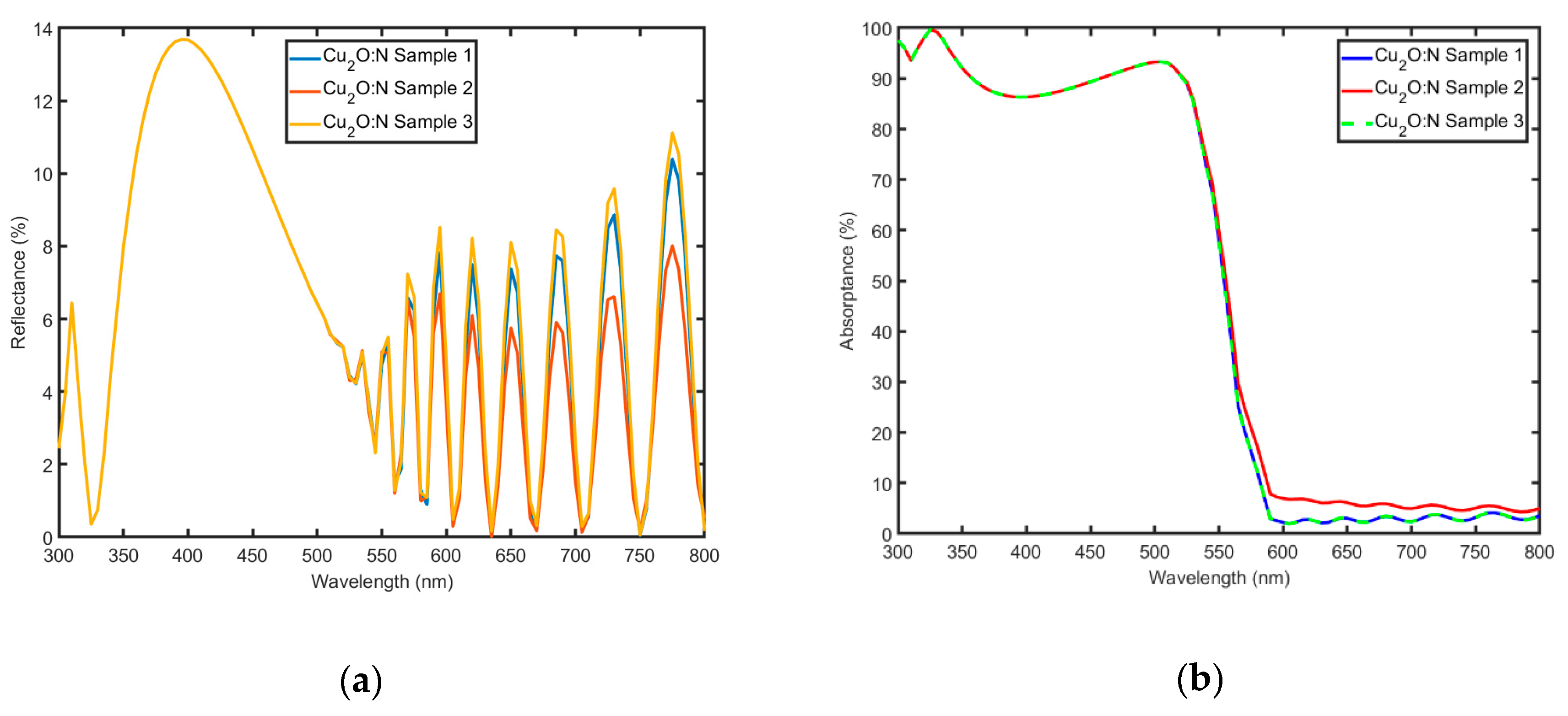
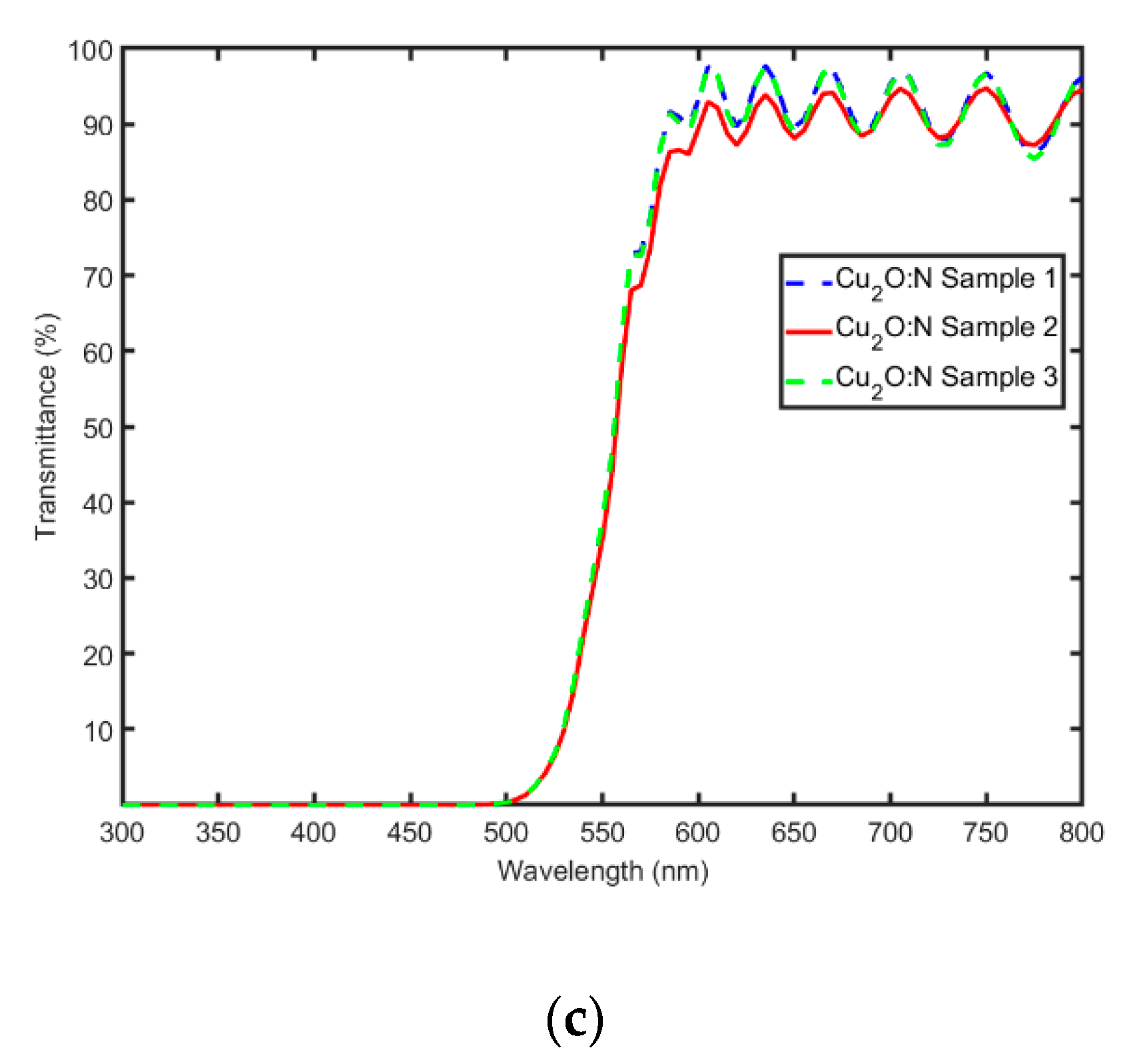
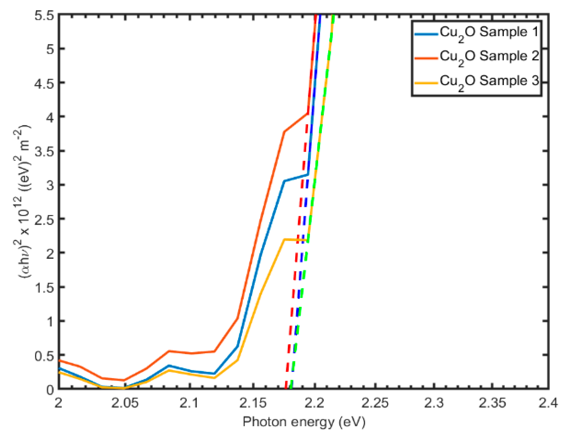
3.3. Optical Characterization

Optical characterization involved two tools: FTIR spectroscopy and spectroscopic ellipsometry. FTIR spectroscopy analysis was carried out using a Perkin Elmer type Spectrum 100 spectrometer, with UATR accessory—PIKE GladiATR, in the wavenumber range 430–2000 cm−1 with a spectral resolution of 0.4 cm−1. The refractive index and extinction coefficient of Cu2O:N thin film were determined by spectroscopic ellipsometry, in the wavelength range from 190 to 2100 nm using an UVISEL spectroscopic ellipsometer from HORIBA Jobin Yvon. A model fit to the measured ellipsometry parameters was obtained using DeltaPsi 2.6 software (Version 2.6, HORIBA, Jobin Yvon, Palaiseau, France).

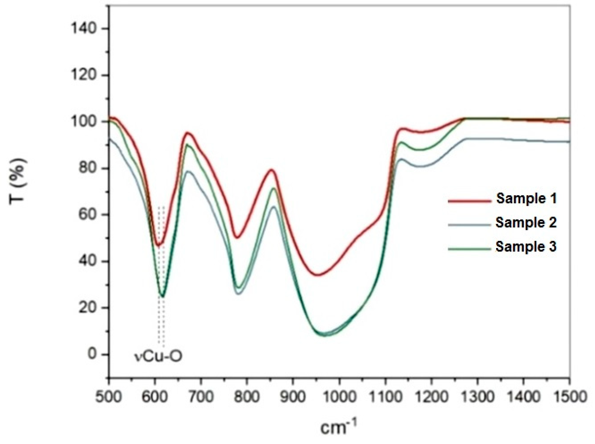
3.3.1. FTIR Spectroscopy

The FTIR transmission spectra obtained for Cu2O:N thin films are shown in Figure 14 and the transmission peaks are listed in Table 4.
The FTIR spectra of all samples deposited on quartz displayed the peaks corresponding to the vibrational modes of Si-O belonging to the quartz substrate (780 cm−1, broadband centered at 980 cm−1 with a shoulder at 1080 cm−1) [26,27]. The band located at 608–616 cm−1 corresponds to the stretching vibrational mode of Cu-O in Cu2O phase. There is an increasing trend in the intensity of the Cu-O absorption band from Sample 1 to Sample 3, suggesting an increased concentration of N2. This result is in agreement with the recent theoretical predictions that nitrogen mainly substitutes Cu in the molecular form, (N2) Cu, in N-doped Cu2O rather than as substitutional N on the O site, (NO) [5]. The decrease in resistivity, coherently with the increase in N doping concentration, was explained by annealing-driven substitution of oxygen atoms with implanted N atoms. The N doping may induce any definite variation in energy band structure of Cu2O films [25].
In general, the photoluminescence (PL) spectra of Cu2O films contain two main signals ranging from 450 to 650 nm, which are considered to be derived from free excitons and the bound excitonic region [28].

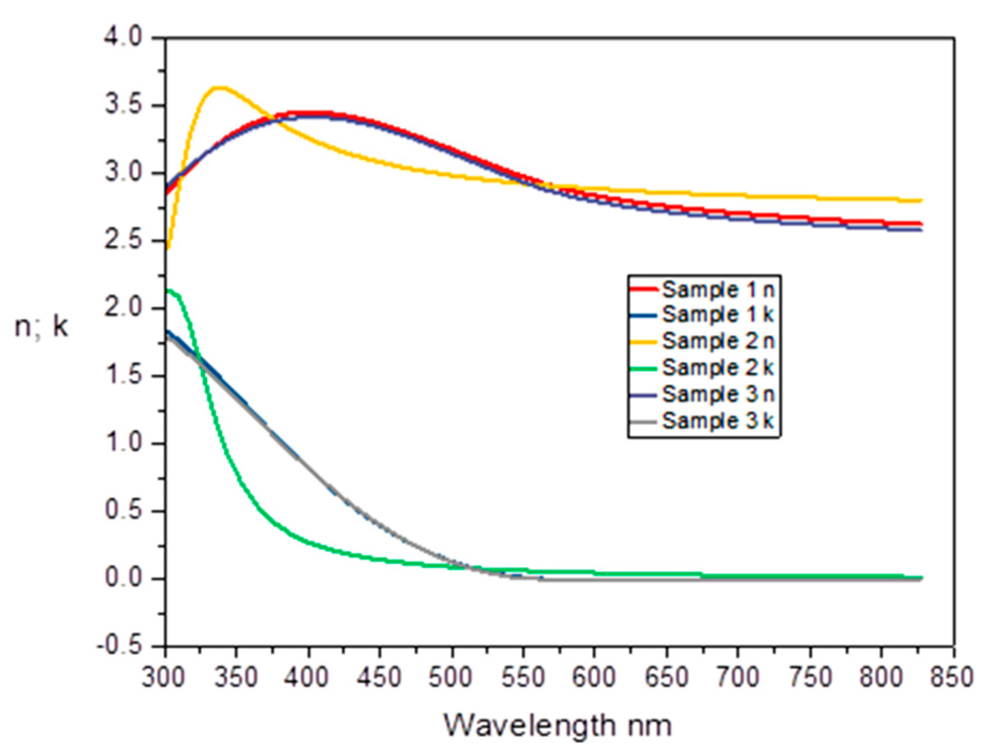
3.3.2. Spectroscopic Ellipsometry (SE)

The ellipsometry parameters of Cu2O:N thin films deposited on quartz substrate were investigated with a resolution of 27 points in the range 1.5–4.1 eV (with step 0.1 eV). The investigated parameters were the band gap and the surface roughness [29,30] and were listed in Table 5.
By the Tauc–Lorentz oscillator methodology [31], modeling was performed to determine the band gap, surface roughness, refractive index (n), and the extinction coefficient (k) in the range 300–800 nm (from visible to near infrared) for Cu2O thin films deposited on quartz substrates.
The model described a layer of Cu2O deposited on the quartz substrate with a hard surface layer. The surface roughness was modeled by mixing the optical constants of the Cu2O material surface and the air voids (on average, 90% Cu2O and 10% air voids).
It is noticed that the surface roughness of Cu2O film increases with the level of N2 pressure (Sample 1 and Sample 3 vs. Sample 2), from 15.9 nm to 19.6 nm (Table 5).
The presence of N2 during deposition of Cu2O films on quartz substrate produces small changes over n and k in the range 300–600 nm for Samples 1–3 and 300–400 nm for Sample 2, as can be seen in Figure 15.
The changes of n(λ) (yellow curve) and k(λ) (green curve) coefficients observed in Figure 15 for Sample 2 (the highest N-doped sample) are associated with a structural change in Cu2O induced by nitrogen doping. This can be a promising method for modifying the optical properties of the metal oxide [28,32] The crystal size decreases from approximately 23 nm to approximately 15 nm with increasing the N-doping concentration in the small N-doping range, where as it is almost unchanged (18–20 nm) in the heavy N-doping range [26].
For example, undoped Cu2O films were deposited on quartz substrates by the RF magnetron sputtering system with a Cu2O target (99.99%, purity); with the Ar flow rate at 20 sccm, the average transmittances in the visible range were 40–60%, and the band gap of Cu2O films was approx. 18 eV [29].

3.4. General Comments on Experimental Investigation and Prospects of Heterojunction Cuprous Oxide Solar Cells with Nitrogen

The experimental investigation of N-doped Cu2O thin films show they have good potential as an absorber layer for photovoltaic applications:
-
The doped samples are characterized by higher whole carrier densities, lower carrier mobilities, and lower resistivities in comparison with the undoped sample;
-
The SEM images showed the improvement in the size uniformity of the deposited Cu2O layers due to N presence;
-
The AFM measurements determined that the roughness is slightly influenced by the N doping, which could affect the electrical properties of solar cells. The histograms derived from the AFM images showed the surface profile height for the studied Cu2O:N samples and emphasized their roughness deviation;
-
The X-ray analysis of Cu2O films put in evidence that all such films are polycrystalline and nitrogen doping does not show any significant change in the XRD pattern. A reduced resistivity was achieved in the N-doped samples compared to the undoped sample;
-
The FTIR spectra of the samples displayed peaks corresponding to the vibrational modes of Si-O belonging to the quartz substrate;
-
The SE analysis stressed the N influence over the optical properties of the Cu2O thin films. The changes of refraction and extinction coefficients were given by the Cu2O:N thin films associated with the structural change in Cu2O induced by N-doping.
At the same time, it could be remarked that the N-doping can lead to the following on the heterojunction copper oxide solar cells with nitrogen:
-
regulation of the band gap enabling increased transmittance;
-
improved carrier lifetime and transport;
-
increased conversion efficiency of the solar cell device.
All these results highlight the N-doped cuprous oxide heterojunction solar cell as a promising candidate for high efficiency solar devices.

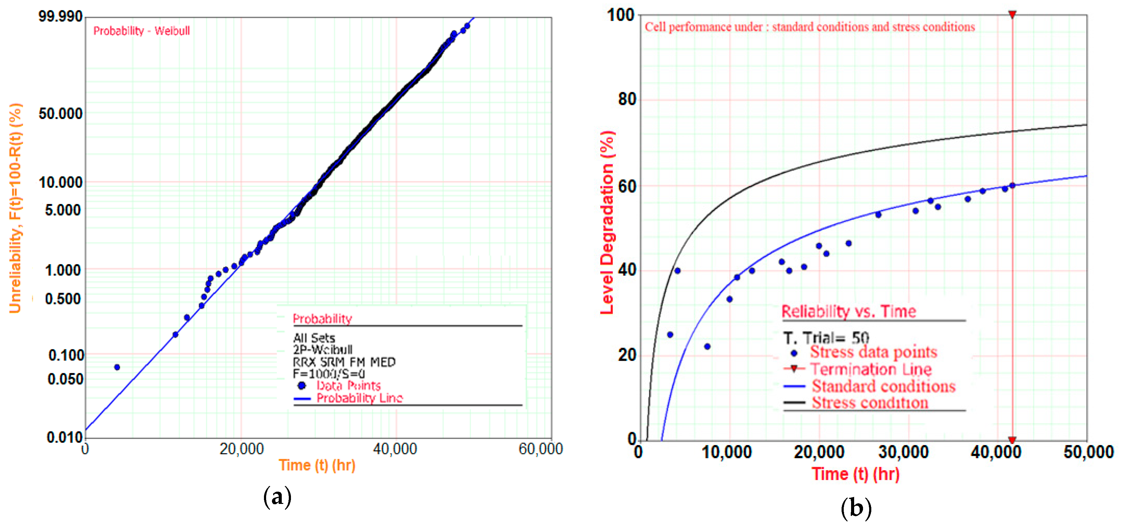
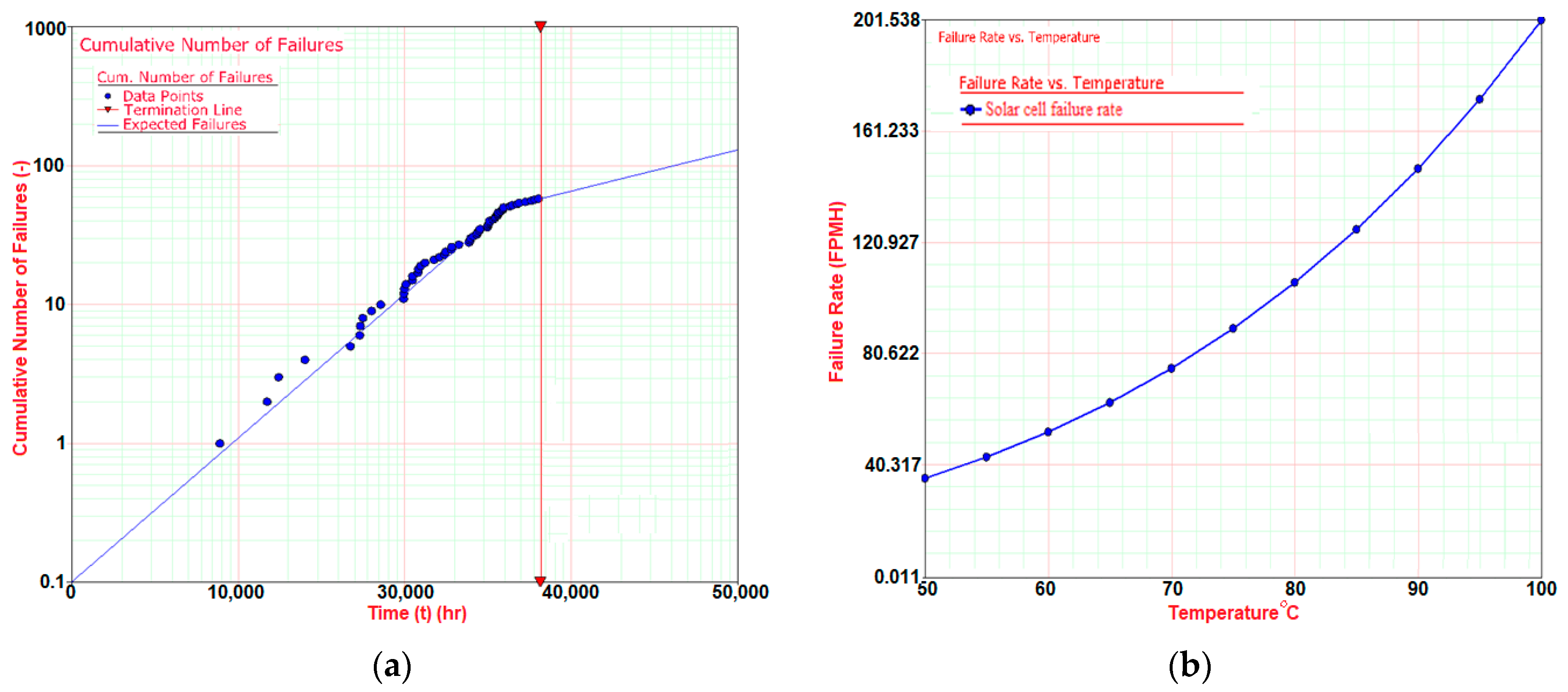
4. Reliability Study

4.1. Methodological Tools

Definition of solar cell reliability: probability of device performance to fit to specific performance parameters for clear operational conditions without deviation outside determined tolerance limits.
There are different accelerated tests to be done regarding the reliability of a solar cell:
(1)
Qualitative accelerated test: offers information regarding the solar cell malfunctions or failure ways;
(2)
High accelerated life test (HALT) offers information regarding the solar cell failure mechanisms and average lifetime;
(3)
High accelerated stress screening (HASS) offers information regarding the solar cell operating time and failure rate within the operating temperature range
In order to perform an accurate reliability analysis of the solar cell, the SYNTHESIS simulation tools developed by ReliaSoft company [33] were used, namely: (1) the Weibull++ tools, which performs life data analysis using multiple lifetime repartitions with a reliability-oriented interface; (2) the ALTA tool, which allows a quantitative analysis of accelerated life tests.

4.2. Solar Cells Thermal Stability Characteristics

Three main parameters can be studied using the Weibull statistical repartition: (1) the solar cell lifetime in different conditions: (2) the degradation degree based on the temperature influence; and (3) number of defects (failures).
In order to make the most accurate predictions for the lifetime of the analyzed solar cells, the Weibull statistical repartition method (Figure 16a) of the Weibull++ tool was employed [33].
The degradation degree of the analyzed solar cell can be characterized by the temperature influence on the device [34,35,36] and is obtained for two cases: (1) under stress conditions (black curve) and (2) under standard conditions (blue curve) (Figure 16b).
Based on the stress results of the HASS test presented in Figure 16b, it is possible to determine, by numerical simulation using the ALTA tool, the limiting value of specific solar cell operating time in normal conditions, as seen in Figure 17a. The HASS test also establishes the probable rate of solar cell failure within the operation temperature range of 50–100 °C (Figure 17b). It is remarked that the expected failures rate dependence increases strongly with temperature.
The simulated results obtained from this reliability analysis consist both in identifying the solar cell failure modes, as well as to predict the solar cell lifetime in normal operation conditions. At the same time, these simulations enable evaluation of the degradation time and number of defects for the analyzed solar cell. The number of defects increases alarmingly starting at 20,000 operating hours, and by the end of the accelerated HASS test, the solar device would fail (Figure 17a).

4.3. Further Work

The simulation tools used in this work, namely Weibull++ and ALTA, have limited capabilities for analyzing different types of advanced solar cells based on different materials. That is why new simulation tools must be considered for a further work dedicated to reliability studies and experimental analyses of metal oxide solar cells. The thermal stability of such devices is essential during solar cell operation. It could be noted that the Cu2O:N layer is very stable because its annealing for 90 min does not degrade its nitrogen-doping, as reported by Ye F. et al. [37].

5. Conclusions

The optimization of a silicon tandem heterojunction solar cell with a Cu2O absorber layer has been analyzed by numerical modeling based on its splitting into two subcells: a ZnO/Cu2O top subcell and a c-Si bottom one. The buffer layer thickness and affinity are essential parameters for implementation of such devices defined by a low conduction band offset.
The optical characteristics of a Cu2O heterojunction solar cell were obtained by numerical modeling, allowing the evaluation of optical losses and determination of maximum absorptance of the device.
A comprehensive characterization (morphological, structural, and optical) of the copper oxide layer with nitrogen doping enables us to propose the metal oxide heterojunction solar cell with nitrogen as a promising candidate for advanced high efficiency solar cells.
The main reliability parameters of metal oxide solar cells, namely the failure rate and degradation degree, were calculated and further work will stress the influence on electrical and optical properties of these devices from the thermal stability point of view.

Author Contributions

Conceptualization, L.F., I.C., and Ø.N.; methodology, L.F., I.C., R.K., and D.C.; formal analysis, L.F.; investigation, L.F., I.C., R.K., C.V., L.B., and D.S.; funding acquisition, L.F. and I.C.; software, S.F. and D.C.; validation, L.F., I.C., Ø.N., J.P.C., and D.C.; resources, I.C., R.K., and L.F.; data curation, S.F.; writing—original draft preparation, L.F., I.C., and S.F.; writing—review and editing, L.F., and I.C.; visualization, L.F. and I.C.; supervision, L.F., I.C., and J.P.C.; project administration, J.P.C., Ø.N., E.M., L.F., and I.C. All authors have read and agreed to the published version of the manuscript.

Funding

This research received no external funding.

Acknowledgments

This work was supported by the project “Multiscale in modelling and validation for solar photovoltaics” (Multiscale Solar) MP1406, 2015–2019, for IPVF (Institute Photovoltaïque de l’Île de France)-GeePs, PUB (Polytechnic University of Bucharest) and INOE, funded by the European Commission through COST program. This research activity was conducted under the research project “High-performance tandem heterojunction solar cells for specific applications (SOLHET)”, for IFE, UiO, PB and INOE funded by the Research Council of Norway (RCN), project no. 251789, and the Romanian Executive Agency for Higher Education, Research, Development and Innovation Funding (UEFISCDI), contracts no. 34/2016 and no. 35/2016, through the M-ERA.NET program, and project no. PN 19_18.01.01/2019, Ad. Act. 2020, for INOE, funded by Ministry of Research and Innovation (MCI), through the NUCLEU program and institutional project 19PFE/2018, Stage IV/2020.

Conflicts of Interest

The authors declare no conflict of interest.

References

  1. Wang, Y.; Miska, P.; Pilloud, D.; Horwat, D.; Mücklich, F.; Pierson, J.F. Transmittance enhancement and optical band gap widening of Cu2O thin films after air annealing. J. Appl. Phys. 2014, 115, 073505. [Google Scholar] [CrossRef]
  2. Jung, Y.S.; Choi, H.W.; Kim, K.H. Properties of p-type N-doped Cu2O thin films prepared by reactive sputtering. Jpn. J. Appl. Phys. 2014, 53, 11RA10. [Google Scholar] [CrossRef]
  3. Siddiqui, H.; Parra, M.R.; Pandey, P.; Singh, N.; Qureshi, M.S.; Haque, F.Z. A review: Synthesis, characterization and cell performance of Cu2O based material for solar cells. Orient. J. Chem. 2012, 28, 1533–1545. [Google Scholar] [CrossRef]
  4. Wang, Y.; Ghanbaja, J.; Horwat, D.; Yu, L.; Pierson, J.F. Nitrogen chemical state in N-doped Cu2O thin films. Appl. Phys. Lett. 2017, 110, 131902. [Google Scholar] [CrossRef]
  5. Sberna, P.M.; Crupi, I.; Moscatelli, F.; Privitera, V.; Simone, F.; Miritello, M. Sputtered cuprous oxide thin films and nitrogen doping by ion implantation. Thin Solid Film. 2016, 600, 71–75. [Google Scholar] [CrossRef]
  6. Mitroi, R.M.; Ninulescu, V.; Fara, L. Tandem solar cells based on Cu2O and c-Si subcells in parallel configuration: Numerical simulation. Int. J. Photoenergy 2017, 2017, 1–6. [Google Scholar] [CrossRef] [Green Version]
  7. Takiguchi, Y.; Miyajima, S. Device simulation of cuprous oxide heterojunction solar cells. Jpn. J. Appl. Phys. 2015, 54, 112303. [Google Scholar] [CrossRef]
  8. Nordseth, O.; Fara, L.; Kumar, R.; Foss, S.E.; Dumitru, C.; Muscurel, V.F.; Drăgan, F.; Crăciunescu, D.; Bergum, K.; Haug, H.; et al. Electro-optical modeling of a ZnO/Cu2O subcell in a silicon-based tandem heterojunction solar cell. In Proceedings of the 33rd European Photovoltaic Solar Energy Conference and Exhibition, Amsterdam, The Netherlands, 25–29 September 2017; pp. 172–177. [Google Scholar] [CrossRef]
  9. Nordseth, O.; Haug, H.; Kumar, R.; Bergum, K.; Drăgan, F.; Craciunescu, D.; Fara, L.; Chilibon, I.; Monakhov, E.; Foss, S.E.; et al. Performance optimization of a four-terminal Cu2O/c-Si Tandem heterojunction solar cell. In Proceedings of the 35th European Photovoltaic Solar Energy Conference and Exhibition, Bruxelles, Belgium, 24–28 September 2018; pp. 29–34. [Google Scholar] [CrossRef]
  10. Dumitru, C.; Fara, L.; Nordseth, O.; Chilibon, I.; Kumar, R.; Svensson, B.G.; Dragan, F.; Muscurel, V.; Craciunescu, D.; Sterian, P. Electro-optical analysis and numerical modeling of Cu2O as the absorber layer in advanced solar cells. In Proceedings of the 2018 International Conference on Photovoltaic Science and Technologies (PVCon), Ankara, Turkey, 4–6 July 2018; pp. 1–7. [Google Scholar] [CrossRef]
  11. Chilibon, I.; Fara, L.; Nordseth, O.; Kumar, R.; Svensson, B.G.; Sterian, P.; Dumitru, C.; Dragan, F.; Muscurel, V.; Vasiliu, C. Structural and electrical analysis of Cu2O layers for solar cell application. Ann. Acad. Rom. Sci. 2018, 11, 53–60. [Google Scholar]
  12. Chilibon, I.; Fara, L.; Nordseth, O.; Kumar, R.; Svensson, B.G.; Sterian, P.; Dumitru, C.; Dragan, F.; Muscurel, V.; Vasiliu, C. Characterization of Cu2O thin films used in solar cells by fluorescence and FTIR spectroscopy. Ann. Acad. Rom. Sci. Ser. Sci. 2018, 11, 61–68. [Google Scholar]
  13. Lloyd, M.A.; Siah, S.C.; Brandt, R.E.; Serdy, J.; Johnson, S.W.; Lee, Y.S.; Buinassisi, T. Intrinsic defect engineering of cuprous oxide to enhance electrical transport properties for photovoltaic applications. In Proceedings of the IEEE 40th Photovoltaic Specialists Conference (PVSC), Denver, CO, USA, 8–13 June 2014; Volume 2016, pp. 3443–3445. [Google Scholar]
  14. Tolstova, Y.; Omelchenko, S.T.; Blackwell, R.E.; Shing, A.M. Polycrystalline Cu2O photovoltaic devices incorporating Zn (O, S) window layers. Sol. Energy Mat. Sol. Cells 2017, 160, 340–345. [Google Scholar] [CrossRef] [Green Version]
  15. Minami, T.; Nishi, Y.; Miyata, T. High-efficiency Cu2O-based heterojunction solar cells fabricated using a Ga2O3 thin film as n-type layer. Appl. Phys. Express 2013, 6, 044101. [Google Scholar] [CrossRef] [Green Version]
  16. Robertson, J.; Falabretti, B. Band offsets of high K gate oxides on III-V semiconductors. J. Appl. Phys. 2006, 100, 014111. [Google Scholar] [CrossRef]
  17. Brandt, R.E.; Young, M.; Hejin, H.P.; Dameron, A.; Chua, D.; Lee, S.Y.; Teeter, G.; Gordon, R.; Buonassisi, T. Band offsets of n-type electron-selective contacts on cuprous oxide (Cu2O) for photovoltaics. Appl. Phys. Lett. 2014, 105, 263901. [Google Scholar] [CrossRef]
  18. PV Lighthouse. Available online: https://www.pvlighthouse.com.au/ (accessed on 20 January 2020).
  19. Baker-Finch, S.C.; McIntosh, K.R. OPAL 2: Rapid optical simulation of silicon solar cells. In Proceedings of the 38th IEEE Photovoltaic Specialists Conference, Austin, TX, USA, 3–8 June 2012; pp. 265–271. [Google Scholar] [CrossRef]
  20. Dumitru, C.; Muscurel, V.; Nordseth, O.; Fara, L.; Sterian, P. Optimization of electro-optical performance and material parameters for a tandem metal oxide solar cell. In Proceedings of the International Conference on Computational Science and Its Applications–ICCSA, Melbourne, Australia, 2–5 July 2018; pp. 573–582. [Google Scholar] [CrossRef]
  21. Murali, D.S.; Kumar, S.; Choudhary, R.J.; Wadikar, A.D.; Jain, M.K.; Subrahmanyam, A. Synthesis of Cu2O from CuO thin films: Optical and electrical properties. AIP Adv. 2015, 5, 047143. [Google Scholar] [CrossRef]
  22. Bennett, J.M.; Mattson, L. Introduction to Surface Roughness and Scattering; Optical Society of America: Washington, DC, USA, 1989. [Google Scholar]
  23. Nordseth, O.; Kumar, R.; Bergum, K.; Chilibon, I.; Fara, L.; Foss, S.E.; Monakhov, E. Nitrogen-doped Cu2O thin films for photovoltaic applications. Materials 2019, 12, 3038. [Google Scholar] [CrossRef] [PubMed] [Green Version]
  24. Lee, S.W.; Lee, Y.S.; Heo, J.; Siah, S.C.; Chua, D.; Brandt, R.; Kim, S.B.; Mailoa, J.P.; Buonassisi, T.; Gordon, R.G. Improved Cu2O-based solar cells using atomic layer deposition to control the Cu oxidation state at the p-n junction. Adv. Energy Mater. 2014, 4, 1301916. [Google Scholar] [CrossRef]
  25. JCPDS 78-2076 for Cu2O, JCPDS 03-0879 for Cu4O3, JCPDS 48-1548 for CuO, and JCPDS 85-1326 for Cu; International Centre for Diffraction Data-JCPDS: Newtown Square, PA, USA, 1996.
  26. Nakano, Y.; Saeki, S.; Morikawa, T. Optical bandgap widening of p-type Cu2O films by nitrogen doping. Appl. Phys. Lett. 2009, 94, 022111. [Google Scholar] [CrossRef] [Green Version]
  27. Reddy, M.H.P.; Pierson, J.F.; Uthanna, S. Structural, surface morphological, and optical properties of nanocrystalline Cu2O and CuO films formed by RF magnetron sputtering: Oxygen partial pressure effect. Phys. Status Solidi A 2012, 209, 1279–1286. [Google Scholar] [CrossRef]
  28. Ogwu, A.A.; Darma, T.H. A reactive magnetron sputtering route for attaining a controlled core-rim phase partitioning in Cu2O/CuO thin films with resistive switching potential. J. Appl. Phys. 2013, 113, 183522. [Google Scholar] [CrossRef]
  29. Su, J.; Niu, Q.; Sun, R.; An, X.; Zhang, Y. Investigation of Cu2O films sputtered with ceramic target: Effect of RF power. J. Optoelectron. Adv. M. 2018, 20, 441–444. [Google Scholar]
  30. Gong, J.B.; Dong, W.L.; Dai, R.C.; Wang, Z.P.; Zhang, Z.M.; Ding, Z.J. Thickness dependence of the optical constants of oxidized copper thin films based on ellipsometry and transmittance. Chin. Phys. B 2014, 23, 1–5. [Google Scholar] [CrossRef]
  31. Gan, J.; Venkatachalapathy, V.; Svensson, B.G.; Monakhov, E.V. Influence of target power on properties of CuxO thin films prepared by reactive radio frequency magnetron sputtering. Thin Solid Film. 2015, 594, 250–255. [Google Scholar] [CrossRef]
  32. Li, J.; Mei, Z.; Liu, L.; Liang, H.; Azarov, A.; Kuznetsov, A.; Liu, Y.; Ji, A.; Meng, Q.; Du, X. Probing defects in nitrogen-doped Cu2O. Sci. Rep. 2014, 4, 7240. [Google Scholar] [CrossRef] [PubMed] [Green Version]
  33. Reliability Engineering Software Products–ReliaSoft. Available online: https://www.reliasoft.com (accessed on 20 January 2019).
  34. Sharma, V.; Chandel, S.S. Performance and degradation analysis for long term reliability of solar photovoltaic systems: A review. Renew. Sustain. Energy Rev. 2013, 27, 753–767. [Google Scholar] [CrossRef]
  35. Guo, D.; Brinkman, D.; Shaik, A.R.; Ringhofer, C.; Vasileska, D. Metastability and reliability of CdTe solar cells. J. Phys. D Appl. Phys. 2018, 51, 15. [Google Scholar] [CrossRef]
  36. Fara, L.; Craciunescu, D. Reliability analysis of photovoltaic systems for specific applications. In Reliability and Ecological Aspects of Photovoltaic Modules; Gok, A., Ed.; Intech Open: London, UK, 2020; pp. 79–92. [Google Scholar]
  37. Ye, F.; Zeng, J.J.; Qiu, Y.B.; Cai, X.M.; Wang, B.; Wang, H.; Zhang, D.P.; Fan, P.; Roy, V.A.L. Deposition-rate controlled nitrogen-doping into cuprous oxide and its thermal stability. Thin Solid Film. 2019, 674, 44–51. [Google Scholar] [CrossRef]
Figure 1. Simplified diagram of the simulated metal oxide solar cell.
Energies 13 04667 g001
Figure 2. AZO (Al:ZnO) thickness vs. top cell efficiency.
Energies 13 04667 g002
Figure 3. Interface defect layer (IDL) thickness vs. top cell efficiency.
Energies 13 04667 g003
Figure 4. Buffer electron mobility (cm2/V∙s) vs. top subcell fill factor and efficiency.
Energies 13 04667 g004
Figure 5. Buffer and IDL affinity vs. subcell efficiency.
Energies 13 04667 g005
Figure 6. Experimental vs. Quokka 2 modeled J-V curve.
Energies 13 04667 g006
Figure 7. Experimental vs. Quokka modeled external quantum efficiency (EQE) curve.
Energies 13 04667 g007
Figure 8. Percentage (a) reflectance, (b) absorptance, and (c) transmittance as a function of wavelength for the metal oxide structure.
Energies 13 04667 g008aEnergies 13 04667 g008b
Figure 9. Tauc plots of Samples 1, 2, and 3 deposited on quartz substrate.
Energies 13 04667 g009
Figure 10. SEM images of Cu2O thin films deposited on quartz substrate: (a) Sample 0, (b) Sample 1, (c) Sample 2, and (d) Sample 3.
Energies 13 04667 g010
Figure 11. 2D AFM images of Samples 0–3 and their corresponding histograms.
Energies 13 04667 g011aEnergies 13 04667 g011b
Figure 12. 3D AFM images of Samples 0–3.
Energies 13 04667 g012aEnergies 13 04667 g012b
Figure 13. XRD patterns of Samples 0–3 in the range 30–60°, where ∆ represents the background peak.
Energies 13 04667 g013
Figure 14. FTIR transmission spectra for Cu2O:N thin film: Sample 1, Sample 2, and Sample 3.
Energies 13 04667 g014
Figure 15. Graphs of n and k coefficients for Samples 1, 2, and 3 of Cu2O:N thin films; λ is wavelength.
Energies 13 04667 g015
Figure 16. (a) Weibull distribution for the studied solar cell lifetime; (b) solar cell performance and degradation degree of the analyzed solar cell under standard and stress conditions.
Energies 13 04667 g016
Figure 17. (a) Cumulative number of failures as function of time (using ALTA module). (b) Baseline survival of solar cell simulation (using ALTA module) in temperature and stress conditions.
Energies 13 04667 g017
Table 1. Experimental J-V fit parameters for the c-Si subcell.
Parameter NameParameter Value
Open circuit voltage, VOC (mV)625.16
Fill Factor, FF (%)76.83
Series resistance, RS (ohm / cm2):0.196
Shunt resistance, RSH (ohm / cm2):2382.8
Table 2. Process characteristics and layer structure of Cu2O:N thin films.
Sample NameGas Flow ConditionsGrains Size (nm)
Sample 0Ar/O2 was fixed at 42.5/7.5 sccm20–90
Sample 1N-doped 1 sccm
(Ar/O2 was fixed at 42.5/7.5 sccm)
20–48
Sample 2N-doped 3 sccm
(Ar/O2 was fixed at 42.5/7.5 sccm)
30–54
Sample 3N-doped 1 sccm
(Ar was varied at 41.5 sccm, O2 was fixed at 7.5 sccm)
40–88
Table 3. RRMS of Cu2O thin films and height distribution standard deviation, derived from histograms of 2D AFM images.
Sample Deposited on QuartzRRMS
(nm)
Height Distribution Standard Deviation (nm)
Sample 06.37.8
Sample 14.75.8
Sample 24.24.5
Sample 33.94.2
Table 4. Transmission peaks for Cu2O:N thin films.
Sample NameνCu2O (cm−1)
Sample 1608
Sample 2616
Sample 3615
Table 5. Investigated (SE) parameters of Cu2O:N thin films.
Sample NameSample 1Sample 2Sample 3
Band gap (eV): 2.172.142.17
Surface roughness (nm): 15.919.617.2

