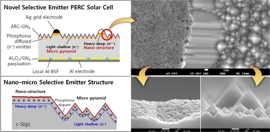
A Novel Method to Achieve Selective Emitter Using Surface Morphology for PERC Silicon Solar Cells


 and
and
Abstract
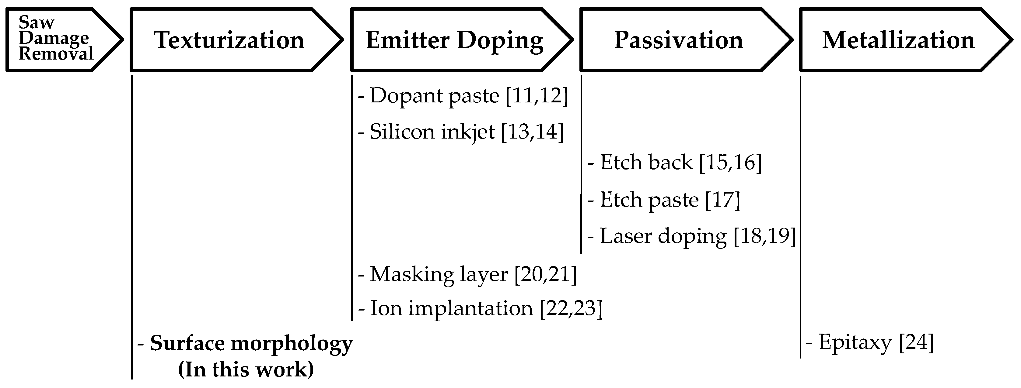
1. Introduction
2. Experimental Details
2.1. Characteristics of Phosphorus Doping According to Nanosurface Morphology
2.2. Characteristics of Nanosurface Emitter Layer According to Doping Condition
2.3. Fabrication of Novel SE Solar Cells Using Surface Morphology
3. Results
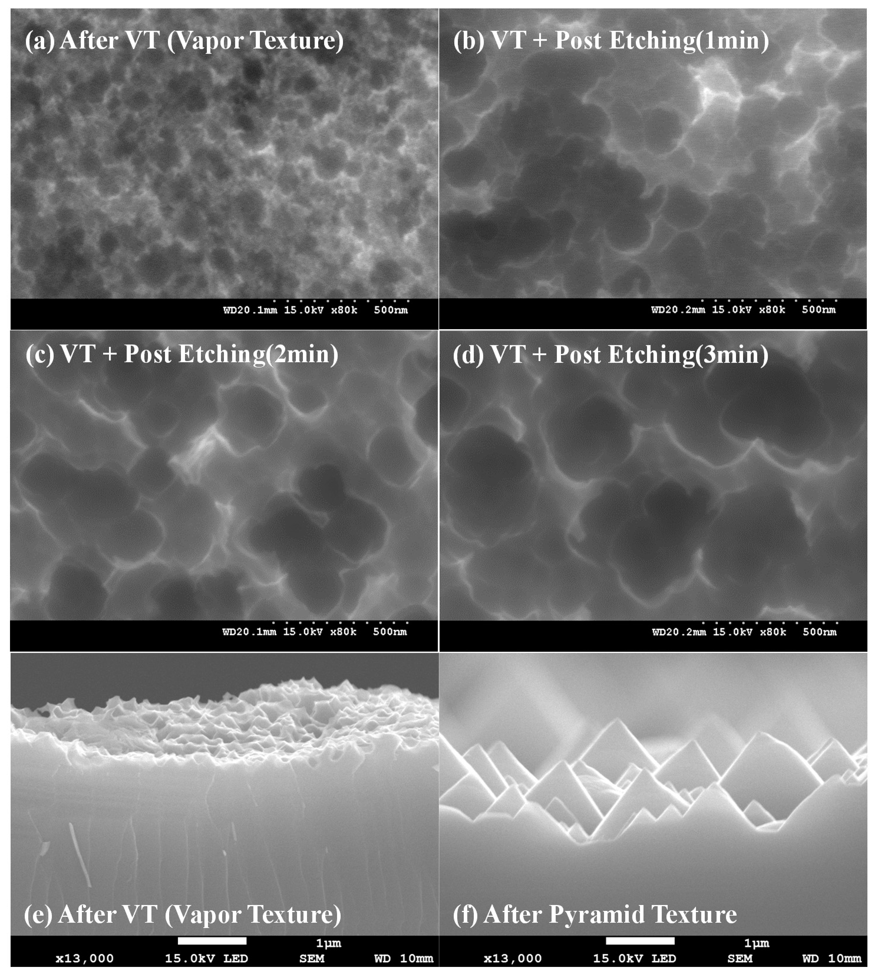
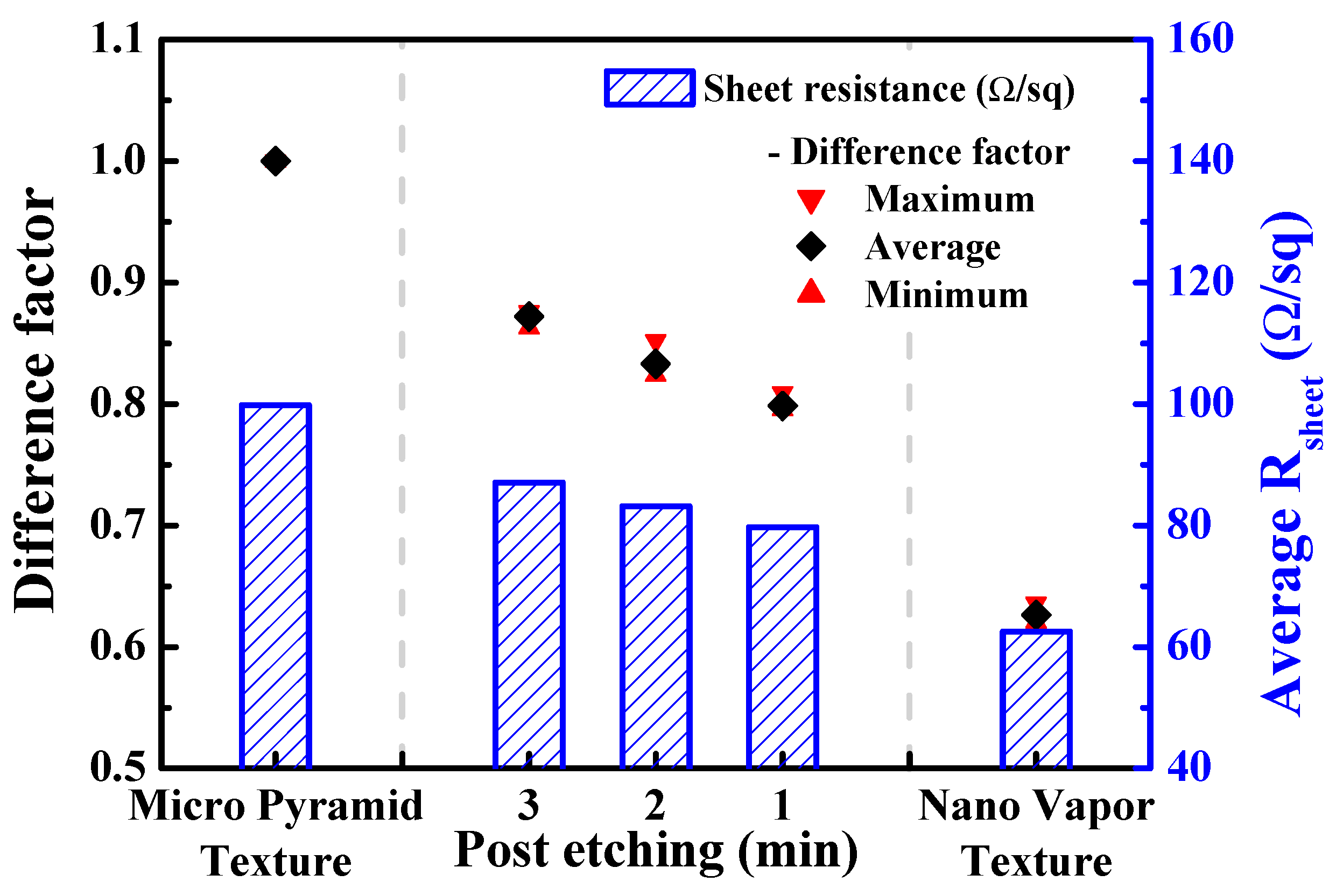
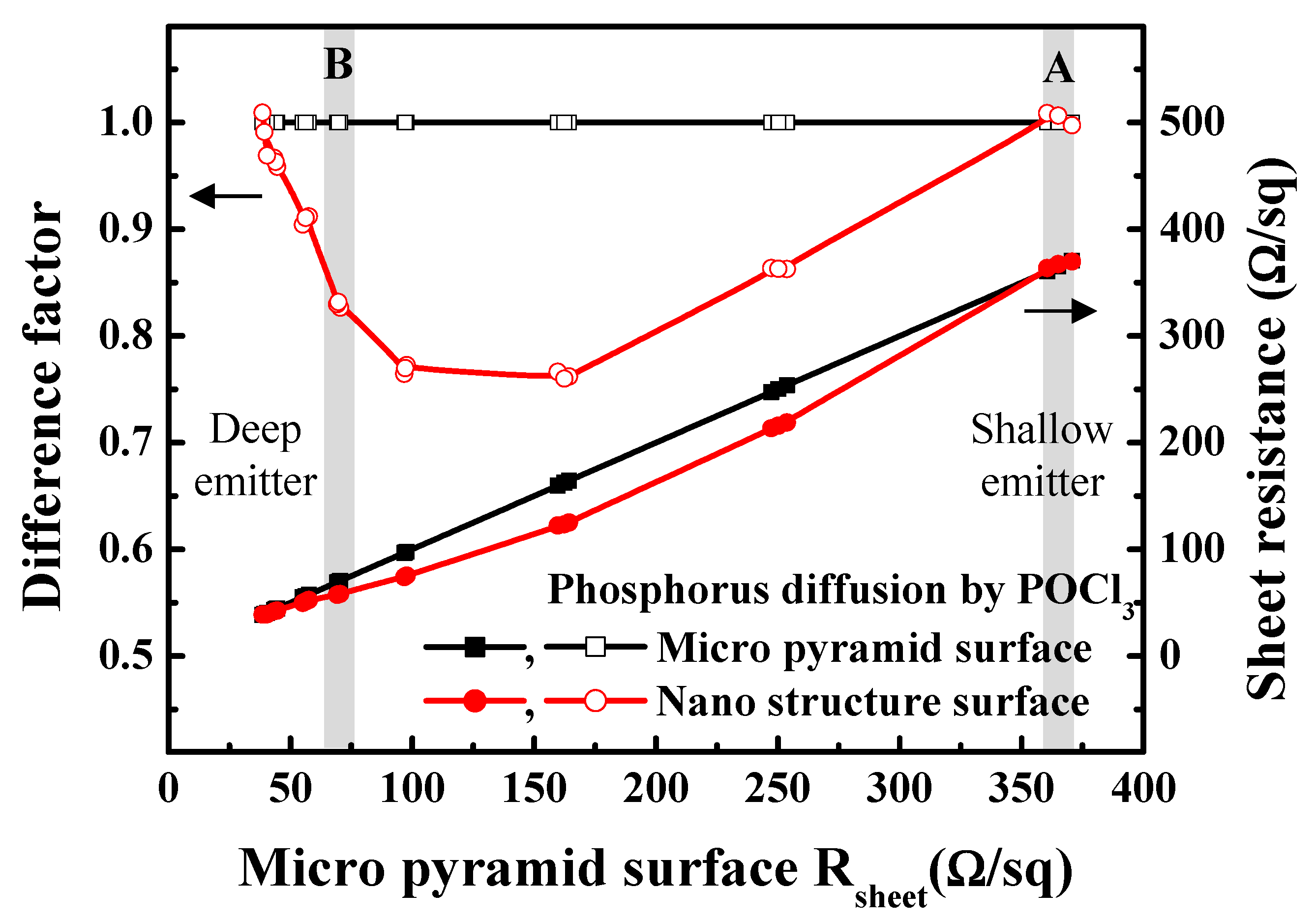
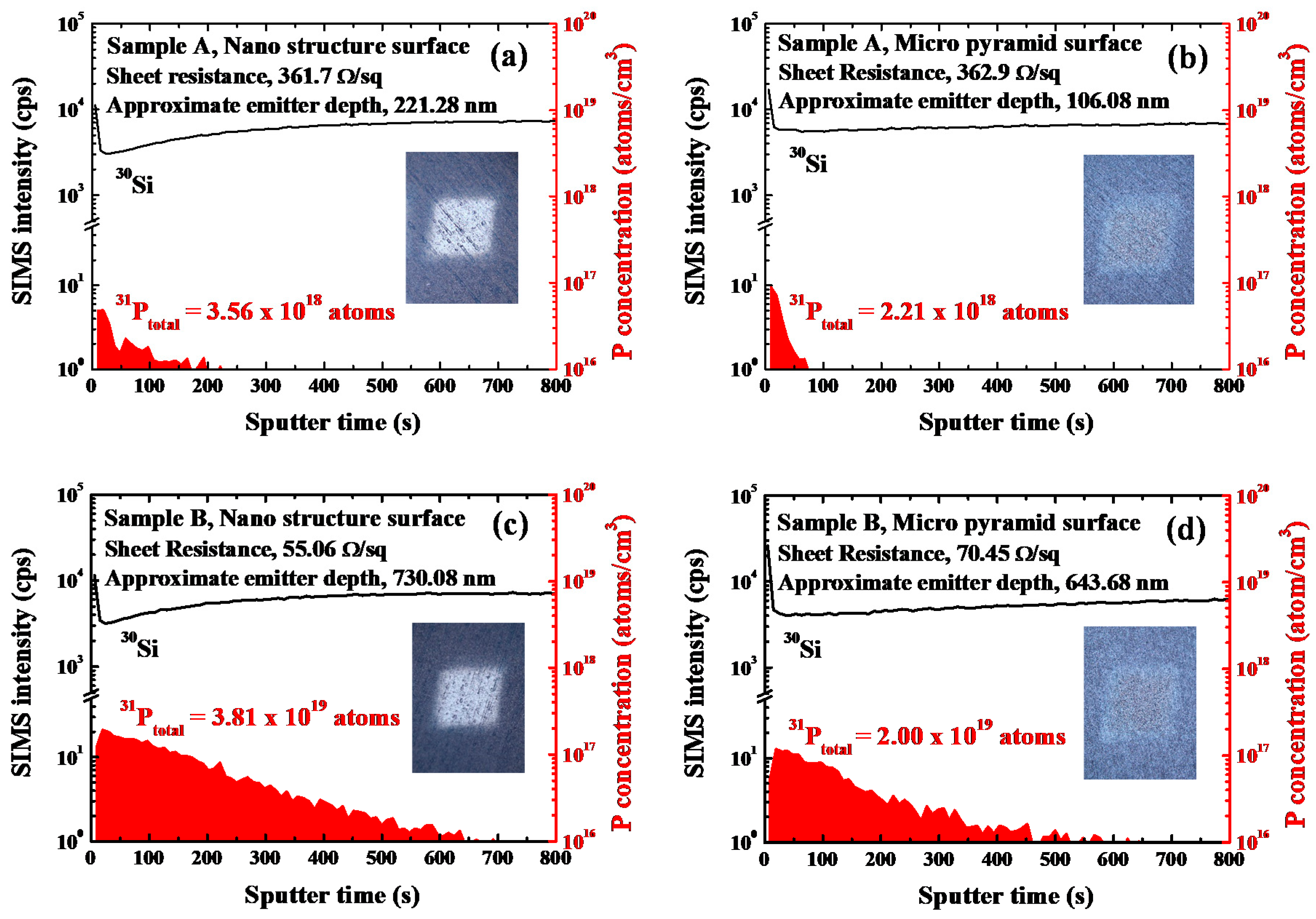
3.1. Characteristics of Phosphorus Doping According to Nanosurface Morphology
3.2. Characteristics of Phosphorus Doping According to Nanosurface Morphology
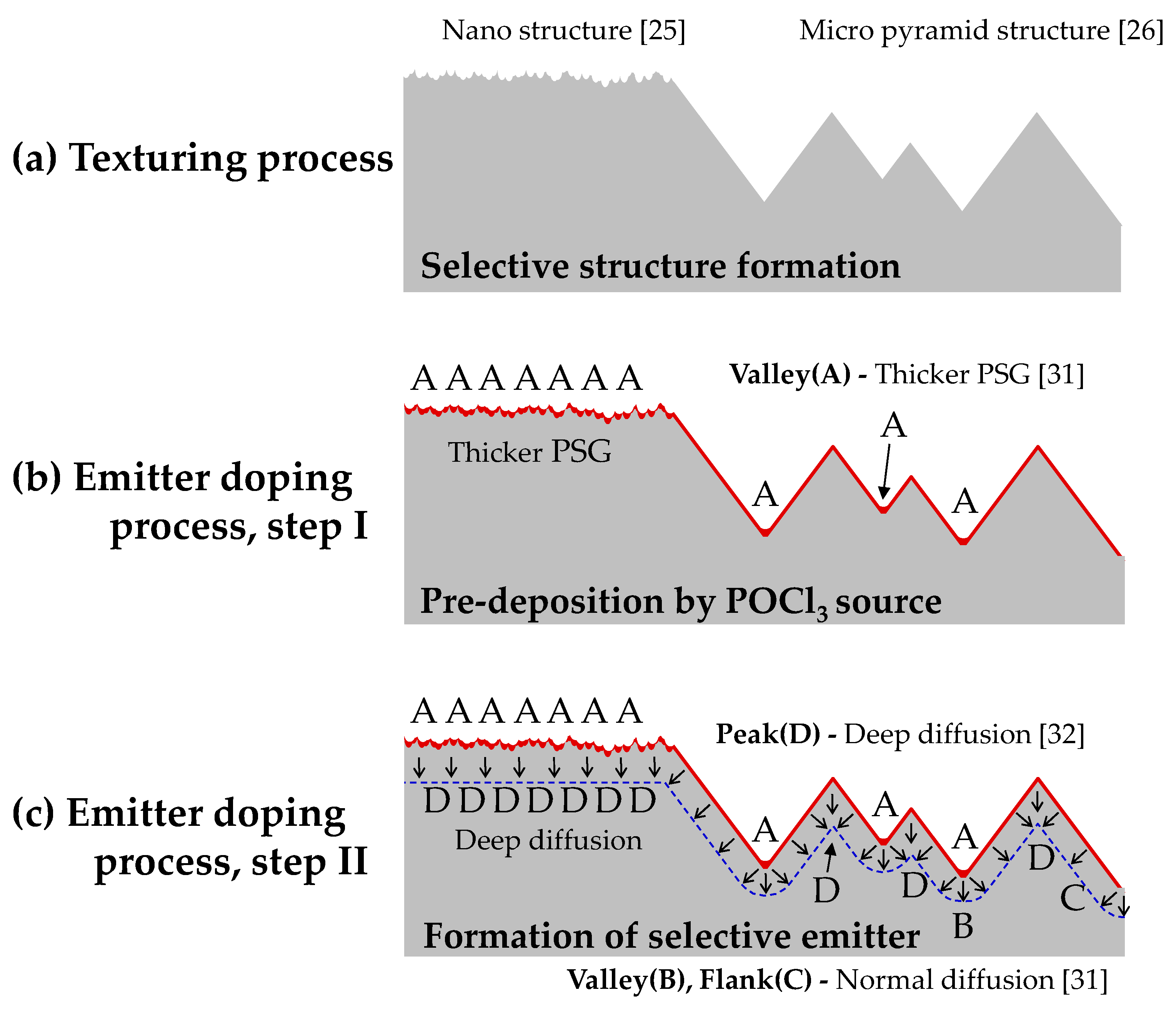
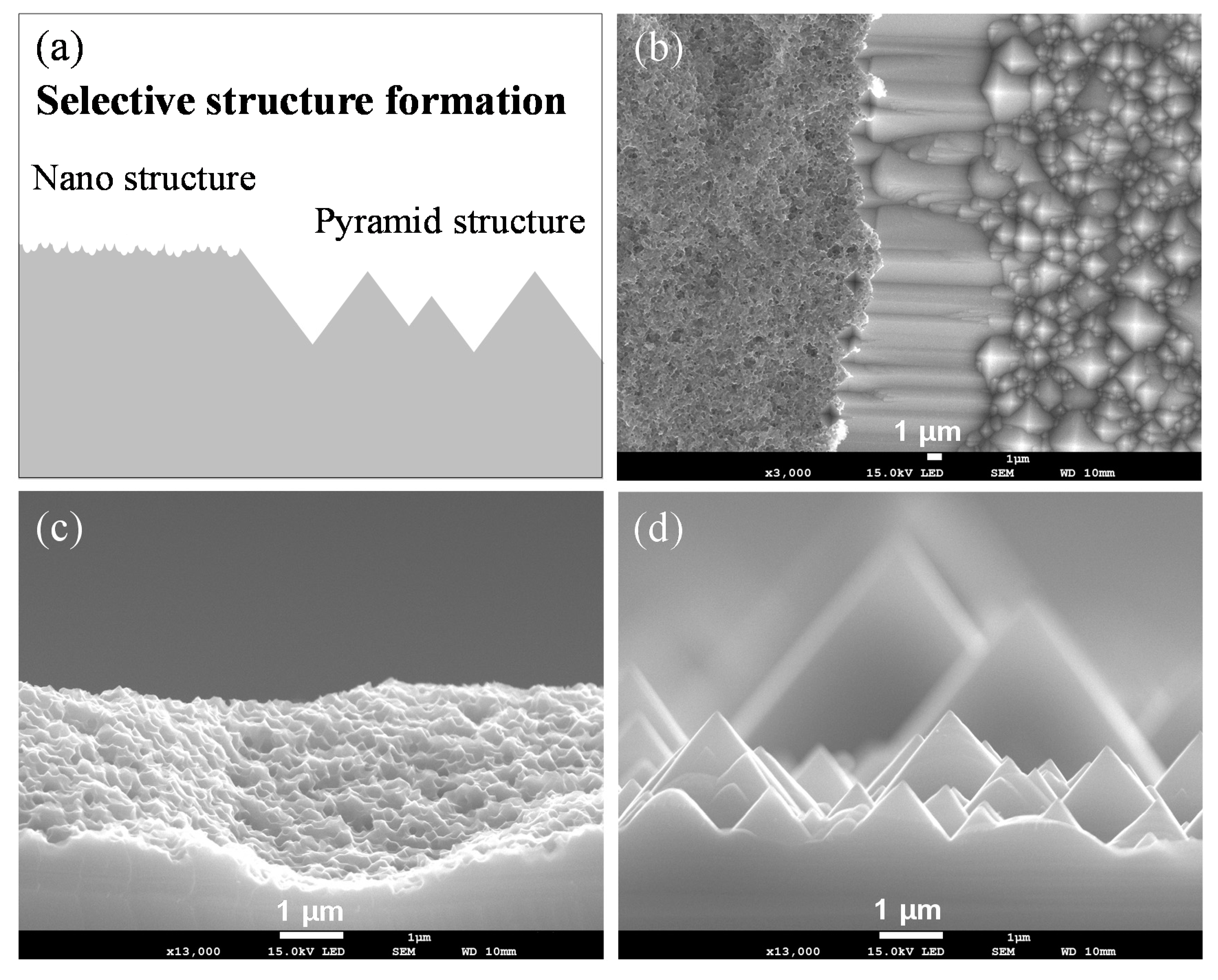
3.3. Mechanism of SE Formation by Nano–Micro-Morphology
3.4. Fabrication of Novel SE Solar Cell.
4. Conclusions
Author Contributions
Funding
Conflicts of Interest
References
- Green, M.A. The path to 25% silicon solar cell efficiency: History of silicon cell evolution. Prog. Photovolt. Res. Appl. 2009, 17, 183–189. [Google Scholar] [CrossRef]
- Swanson, R.M. A vision for crystalline silicon photovoltaics. Prog. Photovolt. Res. Appl. 2006, 14, 443–453. [Google Scholar] [CrossRef]
- ITRPV 2020. International Technology Roadmap for Photovoltaic (ITRPV) Eleventh Edition—2019 Results; ITRPV: Frankfurt, Germany, 2020. [Google Scholar]
- Gassenbauer, Y.; Ramspeck, K.; Bethmann, B.; Dressler, K.; Moschner, J.D.; Fiedler, M.; Brouwer, E.; Drößler, R.; Lenck, N.; Heyer, F.; et al. Rear-Surface Passivation Technology for Crystalline Silicon Solar Sells: A Versatile Process for Mass Production. IEEE J. Photovolt. 2013, 3, 125–130. [Google Scholar] [CrossRef]
- Green, M.A. The passivated emitter and rear cell (PERC): From conception to mass production. Sol. Energy Mater. Sol. Cells 2015, 143, 190–197. [Google Scholar] [CrossRef]
- Chunduri, S.K.; Schmela, M. High Efficiency Cell Technologies 2019 From PERC to Passicated Contacts and HJT. Taiyang News, 2019. [Google Scholar]
- Min, B.; Wagner, H.; Müller, M.; Neuhaus, H.; Brendel, R.; Altermatt, P.P. Incremental efficiency improvements of mass-produced PERC cells up to 24%, predicted solely with continuous development of existing technologies and wafer materials. In Proceedings of the 31st European Photovoltaic Solar Energy Conference and Exhibition, Hamburg, Germany, 14–18 September 2015; pp. 473–476. [Google Scholar]
- Hahn, G. Status of selective emitter technology. In Proceedings of the 25th European Photovoltaic Solar Energy Conference and Exhibition and 5th World Conference on photovoltaic Energy Conversion, Munich, Germany, 6–10 September 2010; pp. 1091–1096. [Google Scholar]
- Rahman, M.Z. Status of selective emitters for p-type c-Si solar cells. Opt. Photonics J. 2012, 2, 129–134. [Google Scholar] [CrossRef][Green Version]
- Lv, Y.; Zhuang, Y.F.; Wang, W.J.; Wei, W.W.; Sheng, J.; Zhang, S.; Shen, W.Z. Towards high-efficiency industrial p-type mono-like Si PERC solar cells. Sol. Energy Mater. Sol. Cells 2020, 204, 110202. [Google Scholar] [CrossRef]
- Tonini, D.; Borrosso, C.; Cellere, G.; Furin, V.; Galiazzo, M.; Kumar, P.; Tanner, D.; Voltan, A. Efficiency gain in c-Si cells through selective emitter and double printing. Energy Procedia 2011, 8, 598–606. [Google Scholar] [CrossRef]
- Horzel, J.; Szlufcik, J.; Nijs, J.; Mertens, R. A simple processing sequence for selective emitters [Si solar cells]. In Proceedings of the Conference Record of the Twenty Sixth IEEE Photovoltaic Specialists Conference, Anaheim, CA, USA, 29 September–3 October 1997; pp. 139–142. [Google Scholar]
- Antoniadis, H. Silicon ink high efficiency solar cells. In Proceedings of the 34th IEEE Photovoltaic Specialists Conference, Philadelphia, PA, USA, 7–12 June 2009; pp. 000650–000654. [Google Scholar]
- Zhong, S.; Shen, W.; Liu, F.; Li, X. Mass production of high efficiency selective emitter crystalline silicon solar cells employing phosphorus ink technology. Sol. Energy Mater. Sol. Cells 2013, 117, 483–488. [Google Scholar] [CrossRef]
- Lauermann, T.; Book, F.; Dastgheib-Shirazi, A.; Hahn, G.; Haverkamp, H.; Bleidiessel, R.; Fleuster, M. The optimal choice of the doping levels in an inline selective emitter design for screen printed multicrystalline silicon solar cells. In Proceedings of the 24th European Photovoltaic Solar Energy Conference and Exhibition, Hamburg, Germany, 21–24 September 2009; pp. 1795–1797. [Google Scholar]
- Basu, P.K.; Cunnusamy, J.; Sarangi, D.; Boreland, M.B. Novel selective emitter process using non-acidic etch-back for inline-diffused silicon wafer solar cells. Renew. Energy 2014, 66, 69–77. [Google Scholar] [CrossRef]
- Book, F.; Raabe, B.; Hahn, G. Two diffusion step selective emitter: Comparison of mask opening by laser or etching paste. In Proceedings of the 23rd European Photovoltaic Solar Energy Conference and Exhibition, Valencia, Spain, 1–5 September 2008; pp. 1546–1549. [Google Scholar]
- Engelhardt, J.; Kromer, H.; Hahn, G.; Terheiden, B. Laser doping from as-deposited CVD layers for high-efficiency crystalline silicon solar cells. In Proceedings of the Silicon PV 2019, the 9th International Conference on Crystalline Silicon Photovoltaics, Leuven, Belgium, 8–10 April 2019; Volume 2147, p. 070002. [Google Scholar]
- Kim, M.; Kim, D.; Kim, D.; Kang, Y. Influence of laser damage on the performance of selective emitter solar cell fabricated using laser doping process. Sol. Energy Mater. Sol. Cells 2015, 132, 215–220. [Google Scholar] [CrossRef]
- Raabe, B.; Haverkamp, H.; Book, F.; Dastgheib-Shirazi, A.; Moll, R.; Hahn, G. Monocrystalline silicon: Future cell concepts. In Proceedings of the 22nd European Photovoltaic Solar Energy Conference and Exhibition, Milano, Italy, 3–7 September 2007; pp. 1024–1029. [Google Scholar]
- Pal, B.; Ray, S.; Gangopadhyay, U.; Ray, P.P. Novel technique for fabrication of n-type crystalline silicon selective emitter for solar cell processing. Mater. Res. Express 2019, 6, 075523. [Google Scholar] [CrossRef]
- Low, R.; Gupta, A.; Bateman, N.; Ramappa, D.; Sullivan, P.; Skinner, W.; Mullin, J.; Peters, S.; Weiss-Wallrath, H. High efficiency selective emitter enabled through patterned ion implantation. In Proceedings of the 35th IEEE Photovoltaic Specialists Conference, Honolulu, HI, USA, 20–25 June 2010; pp. 001440–001445. [Google Scholar]
- Dubé, C.E.; Tsefrekas, B.; Buzby, D.; Tavares, R.; Zhang, W.; Gupta, A.; Low, R.J.; Skinner, W.; Mullin, J. High efficiency selective emitter cells using patterned ion implantation. Energy Procedia 2011, 8, 706–711. [Google Scholar] [CrossRef][Green Version]
- Payo, M.R.; Li, Y.; Russell, R.; Singh, S.; Filipek, I.K.; Duerinckx, F.; Szlufcik, J.; Poortmans, J. Efficiency gain in plated bifacial n-type PERT cells by means of a selective emitter approach using selective epitaxy. Sol. Energy Mater. Sol. Cells 2020, 204, 110173. [Google Scholar] [CrossRef]
- Ju, M.; Balaji, N.; Lee, Y.; Park, C.; Song, K.; Choi, J.; Yi, J. Novel vapor texturing method for EFG silicon solar cell applications. Sol. Energy Mater. Sol. Cells 2012, 107, 366–372. [Google Scholar] [CrossRef]
- Ju, M.; Balaji, N.; Park, C.; Nguyen, H.T.T.; Cui, J.; Oh, D.; Jeon, M.; Kang, J.; Shim, G.; Yi, J. The effect of small pyramid texturing on the enhanced passivation and efficiency of single c-Si solar cells. RSC Adv. 2016, 6, 49831–49838. [Google Scholar] [CrossRef]
- Komatsu, Y.; Harata, D.; Schuring, E.W.; Vlooswijk, A.H.G.; Katori, S.; Fujita, S.; Venema, P.R.; Cesar, I. Calibration of electrochemical capacitance-voltage method on pyramid texture surface using scanning electron microscopy. Energy Procedia 2013, 38, 94–100. [Google Scholar] [CrossRef][Green Version]
- Li, H.; Ma, F.; Hameiri, Z.; Wenham, S.; Abbott, M. On elimination of inactive phosphorus in industrial POCl3 diffused emitters for high efficiency silicon solar cells. Sol. Energy Mater. Sol. Cells 2017, 171, 213–221. [Google Scholar] [CrossRef]
- Kafle, B.; Schön, J.; Fleischmann, C.; Werner, S.; Wolf, A.; Clochard, L.; Duffy, E.; Hofmann, M.; Rentsch, J. On the emitter formation in nanotextured silicon solar cells to achieve improved electrical performances. Sol. Energy Mater. Sol. Cells 2016, 152, 94–102. [Google Scholar] [CrossRef]
- Es, F.; Baytemir, G.; Kulakci, M.; Turan, R. Metal-assisted nano-textured solar cells with SiO2/Si3N4 passivation. Sol. Energy Mater. Sol. Cells 2017, 160, 269–274. [Google Scholar] [CrossRef]
- Voyer, C.; Buettner, T.; Bock, R.; Biro, D.; Preu, R. Microscopic homogeneity of emitters formed on textured silicon using in-line diffusion and phosphoric acid as the dopant source. Sol. Energy Mater. Sol. Cells 2009, 93, 932–935. [Google Scholar] [CrossRef]
- Dastgheib-Shirazi, A.; Steyer, M.; Micard, G.; Wagner, H.; Altermatt, P.P.; Hahn, G. Relationships between diffusion parameters and phosphorus precipitation during the POCl3 diffusion process. Energy Procedia 2013, 38, 254–262. [Google Scholar] [CrossRef]
- Shanmugam, V.; Cunnusamy, J.; Khanna, A.; Basu, P.K.; Zhang, Y.; Chen, C.; Stassen, A.F.; Boreland, M.B.; Mueller, T.; Hoex, B.; et al. Electrical and microstructural analysis of contact formation on lightly doped phosphorus emitters using thick-film Ag screen printing pastes. IEEE J. Photovolt. 2013, 4, 168–174. [Google Scholar] [CrossRef]
- Yang, Y.; Seyedmohammadi, S.; Kumar, U.; Gnizak, D.; Graddy, E.; Shaikh, A. Screen printable silver paste for silicon solar cells with high sheet resistance emitters. Energy Procedia 2011, 8, 607–613. [Google Scholar] [CrossRef]
- Ju, M.; Mallem, K.; Dutta, S.; Balaji, N.; Oh, D.; Cho, E.; Cho, Y.H.; Kim, Y.; Yi, J. Influence of small size pyramid texturing on contact shading loss and performance analysis of Ag-screen printed mono crystalline silicon solar cells. Mater. Sci. Semicond. Process. 2018, 85, 68–75. [Google Scholar] [CrossRef]


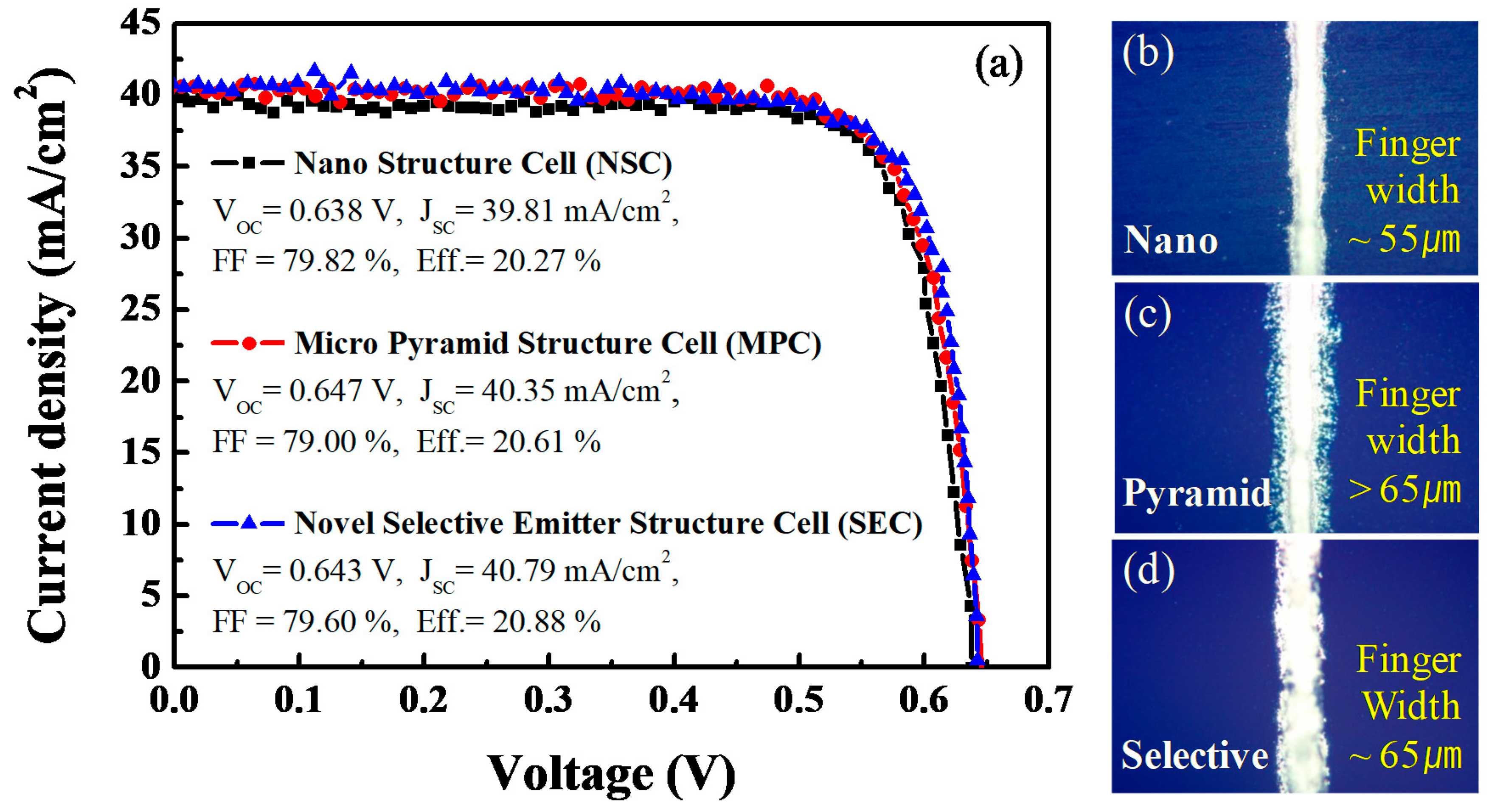
| Light J–V Analysis | Nanostructure Cell (NSC) | Micro-Pyramid Cell (MPC) | SE Cell (SEC) Low/High | |||
|---|---|---|---|---|---|---|
| Sheet Resistance of Emitter (Ω/sq) | 62 | 82 | 62/82 | |||
| Cell remark (9 samples fabricated) | Best | Average | Best | Average | Best | Average |
| JSC (mA/cm2) | 39.81 | 39.07 | 40.35 | 40.24 | 40.79 | 40.63 |
| VOC (V) | 0.638 | 0.637 | 0.647 | 0.643 | 0.643 | 0.642 |
| Fill Factor (%) | 79.82 | 80.18 | 79.00 | 78.61 | 79.60 | 79.29 |
| Efficiency (%) | 20.27 | 19.94 | 20.61 | 20.35 | 20.88 | 20.67 |
© 2020 by the authors. Licensee MDPI, Basel, Switzerland. This article is an open access article distributed under the terms and conditions of the Creative Commons Attribution (CC BY) license (http://creativecommons.org/licenses/by/4.0/).
Share and Cite
Ju, M.; Park, J.; Cho, Y.H.; Kim, Y.; Lim, D.; Cho, E.-C.; Yi, J. A Novel Method to Achieve Selective Emitter Using Surface Morphology for PERC Silicon Solar Cells. Energies 2020, 13, 5207. https://doi.org/10.3390/en13195207
Ju M, Park J, Cho YH, Kim Y, Lim D, Cho E-C, Yi J. A Novel Method to Achieve Selective Emitter Using Surface Morphology for PERC Silicon Solar Cells. Energies. 2020; 13(19):5207. https://doi.org/10.3390/en13195207
Chicago/Turabian StyleJu, Minkyu, Jeongeun Park, Young Hyun Cho, Youngkuk Kim, Donggun Lim, Eun-Chel Cho, and Junsin Yi. 2020. "A Novel Method to Achieve Selective Emitter Using Surface Morphology for PERC Silicon Solar Cells" Energies 13, no. 19: 5207. https://doi.org/10.3390/en13195207
APA StyleJu, M., Park, J., Cho, Y. H., Kim, Y., Lim, D., Cho, E.-C., & Yi, J. (2020). A Novel Method to Achieve Selective Emitter Using Surface Morphology for PERC Silicon Solar Cells. Energies, 13(19), 5207. https://doi.org/10.3390/en13195207